DOI:
10.1039/D0RA04963H
(Paper)
RSC Adv., 2020,
10, 38351-38356
Microwave-assisted calcination of electrospun indium–gallium–zinc oxide nanofibers for high-performance field-effect transistors†
Received
5th June 2020
, Accepted 17th September 2020
First published on 19th October 2020
Abstract
The effects of microwave-assisted calcination of electrospun In–Ga–Zn-O (IGZO) nanofibers intended for electronic devices are unclear. To this end, a systematic study was conducted on the effects of microwave-assisted calcination on the microstructure and optical and mechanical properties of electrospun IGZO nanofibers used in high-performance field-effect transistors (FETs). To clarify the role of microwave annealing (MWA) on the characteristics of the electrospun nanofibers, calcination was carried out using two techniques: MWA and conventional thermal annealing (CTA). The morphological differences between IGZO nanofibers calcined using the two techniques were analyzed by scanning electron microscopy (SEM); the diameter of nanofibers was significantly reduced through MWA as compared to CTA. After calcination, the optical transmittance in the visible region was slightly improved, with the MWA-calcined nanofibers exhibiting a higher transmittance than the CTA-calcined nanofibers. Scratch test results showed that the calcination improved the adhesion strength of the nanofibers to the SiO2 substrate; MWA was more effective in improving the mechanical properties than CTA. Furthermore, the effects of MWA calcination on the electrical properties of FETs fabricated using the electrospun IGZO nanofibers were investigated. The MWA-calcined devices showed better electrical characteristics and reliability than the CTA-calcined devices for IGZO nanofiber FETs.
Introduction
Field-effect transistors (FETs) based on 1D semiconductor nanowires, nanofibers, or nanobelts are extensively studied for future functional devices such as photodetectors, chemical and biological sensors, logic circuits, active matrix organic light emitting diodes, and active channel layers owing to their large surface-to-volume ratio, excellent flexibility, high transparency, and unique crystal structure.1–4 Among the numerous 1D nanomaterials, indium–gallium–zinc oxide (IGZO) nanofibers in particular have received significant attention because of their optical transparency over the visible wavelength range, large specific surface area, and excellent electrical performance.5–7 Electrospinning is widely used for fabricating IGZO nanofibers because it does not require expensive vacuum equipment, and the processing time is relatively short, thus reducing the cost of the process. Moreover, because it is a simple solution-based process, the composition ratio can be easily controlled.8–11 In an electrospinning process, a polymer solution is ejected from a small nozzle under a strong electric field of several kilovolts per centimeter. The accumulation of the static charges on the surface of the droplets induces a jet, resulting in the formation of continuous nanofibers, which randomly gather on the collector surface.12,13 Electrospun IGZO nanofibers incorporated with polymeric organic materials, such as carbon and solvents, exhibit a poor performance as electronic devices, and the weak adhesion due to repeated overlap on the substrate causes the fibers to peel off. Furthermore, the carrier transfer in FETs is confined to a narrow region between the channel and the gate oxide, implying that the interfacial properties of the nanofiber and gate insulator have a significant impact on the performance of IGZO nanofiber FETs.14–16 Therefore, calcination using heat treatment is essential for impurity removal, electrical activation, adhesion, and improvement in mechanical properties of electrospun nanofibers.17,18 Conventional thermal annealing (CTA) using furnaces has been commonly employed in the calcination of nanofibers. However, a fundamental problem of CTA is that it takes a long time for processing and transfers high heat to the samples. An alternative to this method is microwave annealing (MWA) using electromagnetic waves. In MWA, energy is transferred uniformly to the material, regardless of the conduction medium, enabling fast propagation and energy conversion based on rapid heating processes unlike other thermal annealing processes. Depending on the heating mechanism, microwave heating processes have the following advantages: comparatively low temperature process and volumetric and uniform heating from inner materials.19–21 Furthermore, MWA is a very efficient technique because it can selectively heat only IGZO without heating by microwave absorption on plastic substrates or glass substrates. Unlike RTA, MWA also has the advantage of being inexpensive because it uses atmospheric-based process equipment. Accordingly, the volumetric heating properties of MWA provide an efficient calcination process for removing impurities, such as the polymeric organic materials in electrospun IGZO nanofibers and are advantageous for improving adhesion to substrates. Few practical studies on the effects of microwave-assisted calcination on electrospun IGZO nanofibers intended for electronic device applications exist.
Therefore, in this study, we investigated the effects of microwave-assisted calcination on the microstructure and optical and mechanical properties of electrospun IGZO nanofibers. In addition, we fabricated bottom gate-type FETs using the electrospun IGZO nanofibers to analyze the effects of MWA calcination on the electrical properties and reliability of the FETs. The results were compared with that of CTA calcination. Finally, the effects of microwave energy on the defects, traps, electron concentration, and reliability of the electrospun IGZO nanofibers were investigated.
Experimental
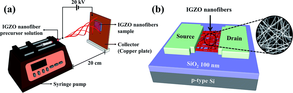
For the preparation of IGZO nanofiber precursor solutions, indium nitrate hydrate [In(NO3)3·xH2O, 99.99%], gallium nitrate hydrate [Ga(NO3)3·xH2O, 99.99%], and zinc acetate dehydrate [Zn(CH3COO)2·2H2O, 99.99%] were dissolved in 0.5 ml of N,N-dimethylformamide (DMF) in a molar ratio of 2![[thin space (1/6-em)]](https://www.rsc.org/images/entities/char_2009.gif) :1:1, and then stirred at 800 rpm for 1 h at room temperature (RT, 25 °C) using a magnetic stirrer. Ethanol-containing polyvinylpyrrolidone (PVP, MW ≈ 1300000) was then added and stirred at 800 rpm for 2 h at RT. All the reagents were purchased from Sigma Aldrich and used without further purification. Subsequently, the prepared precursor solution was loaded into a plastic syringe with a pinhead internal diameter of 0.635 mm; the IGZO nanofiber was electrospun onto a p-type Si substrate with a 100 nm-thick thermally grown SiO2 layer. The experimental setup of the electrospinning system is shown in Fig. 1(a), where the NE-1000 of New Era Pump System is used as the syringe pump. A voltage of 20 kV was applied to the pinhead for electrospinning, and a copper plate placed at distance of 20 cm served as the counter electrode (collector). The syringe pump pressure was set to 0.4 ml h−1, while the temperature and humidity during IGZO nanofiber electrospinning were maintained at 25 °C and 25%, respectively. As a calcination process to remove solvent residuals and polymer matrix in the electrospun IGZO nanofibers, we performed the MWA of 2.45 GHz at 1800 W for 2 min in an air ambient. Our MW irradiation system is shown in Fig. S1,† and the temperature of the MWA measured by an IR thermometer is shown in Fig. S2.† For comparison, the CTA process was carried out at 600 °C for 30 min in O2 ambient. Finally, we fabricated IGZO nanofiber FETs by forming source and drain electrodes through a lift-off process after depositing a 150 nm-thick Ti layer with an e-beam evaporator. The schematic of the IGZO nanofiber FETs is shown in Fig. 1(b). The channel width and length of the fabricated FETs are 10 and 20 μm, respectively.
:1:1, and then stirred at 800 rpm for 1 h at room temperature (RT, 25 °C) using a magnetic stirrer. Ethanol-containing polyvinylpyrrolidone (PVP, MW ≈ 1300000) was then added and stirred at 800 rpm for 2 h at RT. All the reagents were purchased from Sigma Aldrich and used without further purification. Subsequently, the prepared precursor solution was loaded into a plastic syringe with a pinhead internal diameter of 0.635 mm; the IGZO nanofiber was electrospun onto a p-type Si substrate with a 100 nm-thick thermally grown SiO2 layer. The experimental setup of the electrospinning system is shown in Fig. 1(a), where the NE-1000 of New Era Pump System is used as the syringe pump. A voltage of 20 kV was applied to the pinhead for electrospinning, and a copper plate placed at distance of 20 cm served as the counter electrode (collector). The syringe pump pressure was set to 0.4 ml h−1, while the temperature and humidity during IGZO nanofiber electrospinning were maintained at 25 °C and 25%, respectively. As a calcination process to remove solvent residuals and polymer matrix in the electrospun IGZO nanofibers, we performed the MWA of 2.45 GHz at 1800 W for 2 min in an air ambient. Our MW irradiation system is shown in Fig. S1,† and the temperature of the MWA measured by an IR thermometer is shown in Fig. S2.† For comparison, the CTA process was carried out at 600 °C for 30 min in O2 ambient. Finally, we fabricated IGZO nanofiber FETs by forming source and drain electrodes through a lift-off process after depositing a 150 nm-thick Ti layer with an e-beam evaporator. The schematic of the IGZO nanofiber FETs is shown in Fig. 1(b). The channel width and length of the fabricated FETs are 10 and 20 μm, respectively.
 |
| | Fig. 1 (a) Experimental set-up of the electrospinning system, and (b) schematic structure of IGZO nanofiber FETs. | |
The surface morphology of the IGZO nanofibers was analyzed using scanning electron microscopy (SEM; Sirion 400, FEI Company, Hillsboro, OR). The optical properties of the IGZO nanofibers were investigated using an Agilent 8453 ultraviolet-visible (UV-vis) spectrophotometer in the wavelength range of 300–800 nm. The chemical composition of the IGZO NFs was analyzed by X-ray photoelectron spectroscopy (XPS; PHI 5000 Versa Probe II, ULVAC), performed using monochromatic Al-Kα radiation (λ = 0.833 nm). The crystallinity of the IGZO nanofibers were investigated by X-ray diffraction (XRD; SmartLAB, Rigaku Corporation) at 40 kV and 30 mA using Cu-Kα radiation (λ = 0.154 nm) in the conventional Bragg–Brentano configuration. We evaluated the acoustic emission and friction coefficient to determine the critical load using a scratch test apparatus (CP-4, CETR) with a rockwell-shaped diamond indenter. The electrical characteristics were measured using an Agilent 4156 B Precision Semiconductor Parameter Analyzer. All the measurements were performed in a dark box to suppress external light and electrical noise.
Results & discussion
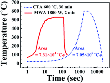
Fig. 2 shows the temperature profiles of the MWA (solid red line) and CTA (blue dashed line) processes applied to the calcination of IGZO nanofibers. Compared to the CTA method, MWA has a shorter calcination time and a faster ramp up and down rate, resulting in a much lower thermal budget, which is expressed as the product of the process time and temperature. In CTA calcination, the IGZO nanofibers are exposed to thermal energy at 600 °C for 30 min and during long ramping up and down steps, resulting in a high thermal budget of 7.05 × 10⁶ °C s. By contrast, in MWA calcination, the IGZO nanofibers are exposed to a thermal energy at 1800 W for 2 min and during short ramping up and down steps. Using an infrared (IR) thermometer, we found the temperature of the sample to be approximately 530 °C under a microwave power of 1800 W, resulting in a low thermal budget of 7.31 × 10⁴ °C s. Therefore, the MWA has a 96.4 times lower thermal budget than the CTA.
 |
| | Fig. 2 Temperature profile of MWA and CTA processes for a-IGZO nanofibers calcination. | |
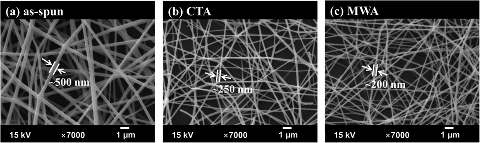
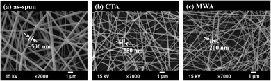
Fig. 3 shows the SEM images of the (a) as-spun, (b) CTA-calcined, and (c) MWA-calcined IGZO nanofibers. The diameter of the IGZO nanofibers shown in the SEM image is the average of 20 randomly selected fibers for each condition. The diameter of the IGZO nanofibers in Fig. 3(a) without calcination (as-spun) is approximately 500 nm, whereas the diameters of the CTA and MWA-calcined nanofibers decrease to approximately 250 and 200 nm, respectively, as shown in Fig. 3(b) and (c). In addition, the smaller diameter of the calcined fibers suggests that MWA is more efficient for PVP removal and IGZO calcination, despite the shorter annealing times and lower temperatures than CTA. As a result, we established a nanofiber calcination technique using a low thermal budget and cost-effective MWA process.
 |
| | Fig. 3 SEM images of (a) as-spun, (b) CTA calcined and (c) MWA calcined IGZO nanofibers. | |
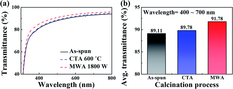
Fig. 4 shows the optical properties of the electrospun IGZO nanofibers before and after the calcination. The optical transmittance spectra of the nanofibers in the wavelength range from 300 to 800 nm are shown in Fig. 4(a), where the transmittance of the calcined nanofibers is found to be slightly improved compared to the as-spun fibers. In the visible wavelength range of 400–700 nm, shown in Fig. 4(b), the as-spun and CTA-calcined IGZO nanofibers exhibit similar average transmittances of 89.11 and 89.78%, respectively. The MWA-calcined nanofibers, on the other hand, exhibit a higher average transmittance of 91.78%.
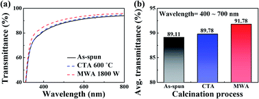 |
| | Fig. 4 (a) Optical transmittance spectra of nanofibers and (b) average transmittance in the visible light wavelength range of 400–700 nm. | |
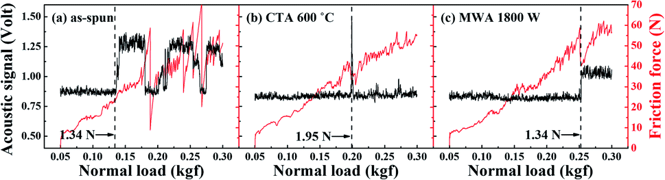
The effects of calcination on the mechanical properties between the IGZO nanofibers and the SiO2 substrate were analyzed by conducting a scratch test, as shown in Fig. 5. The scratch test was conducted based on continuous loading with a normal force ranging from 0.5 to 2.9 N. The samples were scratched by increasing the normal load at a rate of 0.08 N s−1 with a scratching speed of 0.1 mm s−1 for distance of 3 mm. The recorded frictional and acoustic emission signals for the as-spun, CTA, and MWA-calcined fibers are shown in Fig. 5(a), (b) and (c), respectively. The acoustic emission signal consists of an elastic wave generated by a sudden crack in the material when an external load is applied. The fluctuations in the acoustic emission signal indicate the onset of cracking, consistent with the friction data. The irregular pattern observed in the frictional force is probably due to the chipping of the IGZO nanofibers. The critical load of the spun IGZO nanofibers on the SiO2 substrate was 1.34 N but increased to 1.95 N by CTA calcination and 2.41 N by MWA calcination. The average critical load derived from the scratch test showed that the calcination improved the mechanical strength of the IGZO nanofibers and the adhesion to SiO2, with MWA calcination being more effective than CTA calcination.
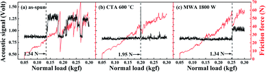 |
| | Fig. 5 Scratch test results for (a) as-spun, (b) CTA-calcined and (c) MWA-calcined IGZO nanofibers. The arrow indicates the critical load at the onset of cracking. | |
Fig. 6 shows a comparison of the effects of MWA and CTA calcination on the electrical properties of bottom gate-type IGZO nanofiber FETs. The transfer characteristic curves (ID–VG) in Fig. 6(a) were measured at a drain voltage (VD) of 10 V, and the gate voltage (VG) was swept from −20 to 40 V. In addition, the output characteristic curves (ID–VD) in Fig. 6(b) were measured at VD = 0 to 20 V and VG − VTH = 0 to 20 V (at 2 V intervals). The device performance largely depends on the calcination method, without which the device performance is very poor, as shown in Fig. 6(a). Compared to the CTA-calcined FETs, the threshold voltage (VTH) of the MWA-calcined FETs shifts to the left in Fig. 6(a), and the drain current increases significantly, as shown in Fig. 6(a) and (b), indicating that MWA increases the carrier concentration in the IGZO nanofiber channel. The additional electrical properties according to the temperature of the CTA and the power of the MWA are shown in Fig. S3.†
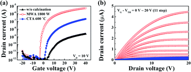 |
| | Fig. 6 (a) Transfer and (b) output characteristic curves of CTA and MWA-calcined IGZO nanofiber FETs. | |
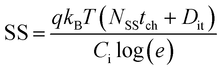
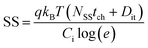
The electrical parameters of the electrospun IGZO nanofiber FETs calcined with MWA and CTA were extracted from the I–V curves and summarized in Table 1. The MWA-calcined IGZO nanofiber FETs showed a field effect mobility (μFE) of 37.6 cm2 V−1 s−1, a sub-threshold swing (SS) of 304.9 mV dec−1, a VTH of −2.8 V, and an on/off current (ION/IOFF) ratio of 4.3 × 10⁶. In comparison, the CTA-calcined IGZO nanofiber FETs exhibited a lower μFE of 1.6 cm2 V−1 s−1, a higher SS of 986.6 mV dec−1, a higher VTH of 3.1 V, and a lower ION/IOFF ratio of 1.9 × 10⁵. In particular, the magnitude of the SS depends on the trap density at the channel/gate dielectric interface (Dit) and the total trap density at the bulk channel layer (NSS), which significantly affects the electrical performance and reliability. Thus, we extracted NSS and Dit from SS as follows:22,23
| |
 | (1) |
where
q is the electron charge,
kB is the Boltzmann's constant,
T is the absolute temperature, and
Ci is the gate dielectric capacitance per unit area, which is estimated to be 3.45 × 10
−8 F cm
−2. To estimate the change in
NSS or
Dit depending on the calcination conditions,
NSS or
Dit is separately set to zero, and thus, the calculated
NSS and
Dit values represent the maximum densities. The MWA and CTA-calcined IGZO nanofiber FETs have
Dit values of 1.1 × 10
12 and 3.6 × 10
12 cm
−2 eV
−1 and
NSS values of 1.6 × 10
17 and 5.1 × 10
17 cm
−3 eV
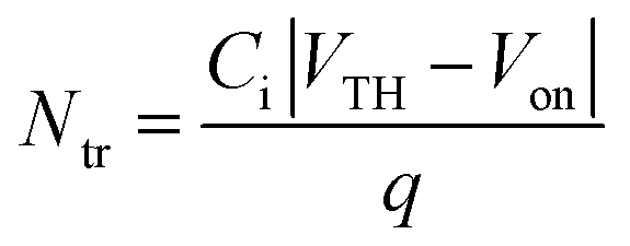
−1, respectively. Furthermore, we extracted the interface electron trap density (
Ntr) and electron concentration (
Nch) from the nanofiber channel using the turn-on voltage (
Von) and the following relationship:
24,25| |
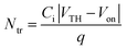 | (2) |
| |
 | (3) |
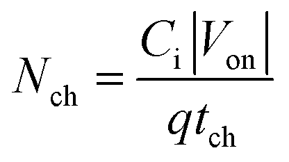
where
tch is the thickness of the channel layer. As a result, as summarized in
Table 1, the extracted
Ntr values of the calcined nanofiber channels are 1.5 × 10
11 and 5.6 × 10
11 cm
−2 for MWA and CTA, and the extracted
Nch values are 3.1 × 10
16 and 5.4 × 10
15 cm
−3 for MWA and CTA, respectively. Thus, MWA-calcined nanofiber FETs has lower
VTH and higher drain drive current (
ID) because
Ntr is lower and
Nch is higher than CTA-calcined nanofiber devices. The electrical properties of the IGZO nanofiber FET, shown in
Fig. 6, suggest that the microwave energy effectively reduces the defects and traps and increases the electron concentration in a short processing time, contributing not only to improved performance but also to improved reliability.
Table 1 Electrical parameters of the electrospun IGZO nanofiber FETs calcined with MWA and CTA and extracted from I–V curves
| |
MWA |
CTA |
| VTH (V) |
−2.8 |
3.1 |
| Nch (cm−3) |
3.1 × 10¹⁶ |
5.4 × 10¹⁵ |
| Ntr (cm−2) |
1.5 × 10¹¹ |
5.6 × 10¹¹ |
| μFE (cm2 V−1 s−1) |
37.6 |
1.6 |
| SS (mV dec−1) |
304.9 |
986.6 |
| ION/IOFF |
4.3 × 10⁶ |
1.9 × 10⁵ |
| Dit (cm−2 eV−1) |
1.1 × 10¹² |
3.6 × 10¹² |
| NSS (cm−3 eV−1) |
1.6 × 10¹⁷ |
5.1 × 10¹⁷ |
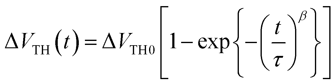
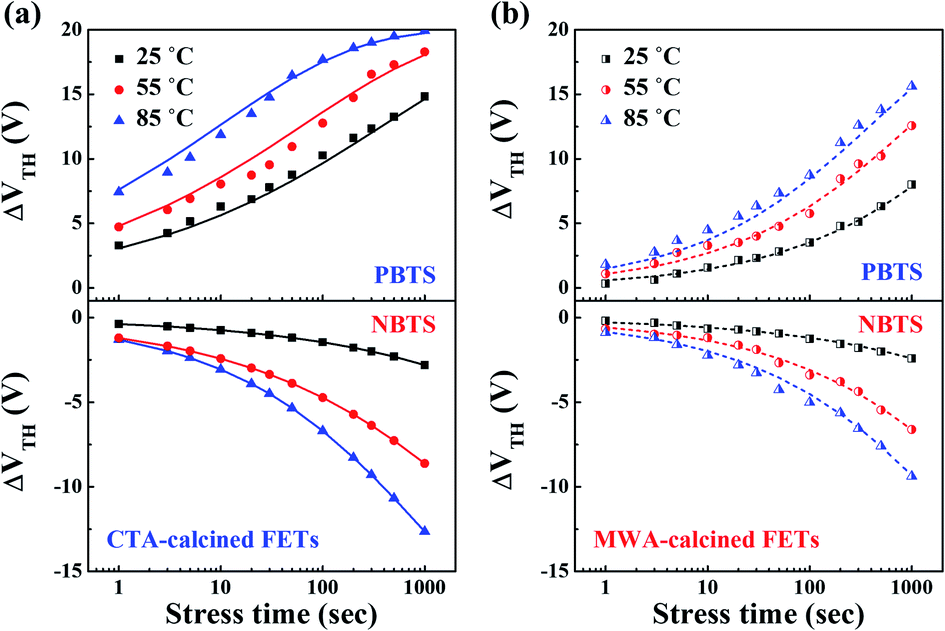
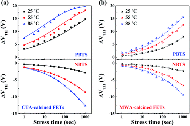
Fig. 7 shows the time dependence of the threshold voltage shift (ΔVTH) under positive bias temperature stress (PBTS) and negative bias temperature stress (NBTS) acting on the IGZO nanofiber FETs with respect to the calcination process. Although the long-term instability is critical for electronic device performance, there are few reports on the reliability of electrospun IGZO nanofiber FETs. In the PBTS and NBTS tests, the measurement conditions were VGS = VTH0 ± 20 V and VDS = 0 V for 103 s at 25–85 °C, where VTH0 is the pristine threshold voltage before gate bias stress. In both the MWA and CTA-calcined devices, VTH shifted toward the positive voltage in PBTS and negative voltage in the NBTS with increasing gate bias stress time. In addition, as the bias stress temperature increased, ΔVTH increased faster with the bias stress time. Comparing Fig. 7(a) and (b), we find that the MWA-calcined devices have lower ΔVTH than the CTA-calcined devices. The threshold voltage instability due to gate bias stresses have been reported to be associated with the trapping of electrons or holes in the trap states present at the channel/gate interface or in the gate insulator bulk.26,27 In other words, positive ΔVTH by PBTS is due to the oxygen-related acceptor-like trap states, whereas negative ΔVTH by NBTS is due to the oxygen pore-related donor-like trap states. We fitted the experimental data for ΔVTH using the following stretched-exponential equation for charge trapping:28
| |
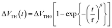 | (4) |
where Δ
VTH0 is the Δ
VTH(
t) at infinite time,
τ is the characteristic trapping time of the carriers,
β is the stretched-exponential exponent, and
t is the stress time. The solid lines in (a) and the dashed lines in (b) fitted with the stretched-exponential equations are in good agreement with the experimental results, indicating that
τ depends on the temperature.
 |
| | Fig. 7 Time dependence of ΔVTH under PBTS and NBTS tests for the electrospun IGZO nanofiber FETs calcined with (a) MWA and (b) CTA. The solid lines in (a) and the dotted lines in (b) represent the curves fitted with the stretched-exponential equation. | |
In the stretched-exponential equation, the characteristic trapping time (τ) of a thermally activated carrier is expressed as:
| |
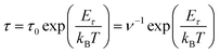 | (5) |
where the thermal activation energy is given by
Ea =
Eτβ;
Eτ is the average effective energy barrier that needs to be overcome before the electrons in the nanofiber channel enter the gate insulator;
τ0 is the thermal prefactor; and
ν is the frequency prefactor for emission across the barrier. The
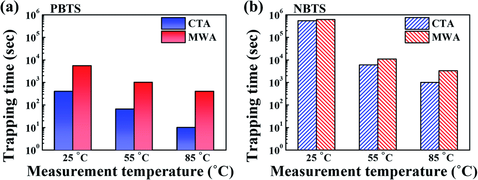
τ value of the IGZO nanofiber FETs calcined with MWA and CTA under (a) PBTS and (b) NBTS tests is shown in
Fig. 8. As the test temperature increases,
τ gradually decreases, and the MWA-calcined IGZO nanofiber FETs have a higher
τ value than the CTA-calcined devices. This indicates that the CTA-calcined IGZO nanofiber FETs trap the carrier faster than the MWA-calcined devices, resulting in long-term reliability issues.
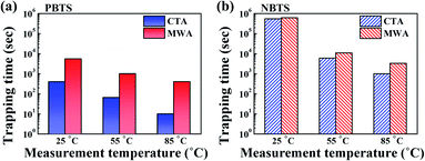 |
| | Fig. 8 Charge trapping time (τ) of IGZO nanofiber FETs calcined with MWA and CTA under (a) PBTS and (b) NBTS tests. | |
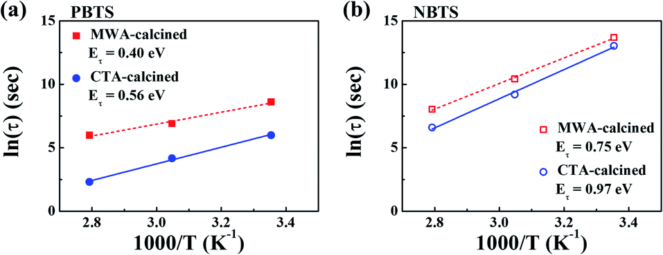
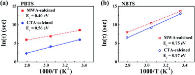
Fig. 9 shows an Arrhenius plot of ln(τ) versus the inverse of the absolute temperature in (a) PBTS and (b) NBTS tests for IGZO nanofiber FETs calcined with MWA and CTA. The linear relationship between ln(τ) and 1/T represents a thermally activated charge trapping process in the IGZO nanofiber FETs, and the slope of the Arrhenius plot represents Eτ for charge transport under the PBTS and NBTS tests. The Eτ value of the MWA-calcined nanofiber FETs is 0.40 eV for PBTS and 0.72 eV for NBTS. The Eτ value of the CTA-calcined nanofiber FETs is 0.56 eV for PBTS and 0.97 eV for NBTS. The magnitude of Eτ is related to the lattice arrangement of the IGZO nanofiber channels. Lower Eτ indicates fewer defects in the channel and a more optimal lattice arrangement, resulting in improved instability.29,30 Therefore, we conclude that MWA calcination is more effective in improving the stability of electrospun IGZO nanofiber devices than CTA calcination.
 |
| | Fig. 9 Arrhenius plots of ln(τ) versus the inverse of the absolute temperature in (a) PBTS and (b) NBTS tests for IGZO nanofiber FETs calcined with MWA and CTA. | |
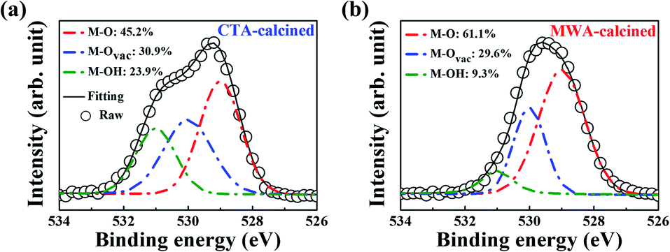
Fig. 10 exhibits the XPS O 1s spectra of the IGZO nanofibers treated by (a) CTA calcination and (b) MWA calcination. XPS analysis was performed to determine the chemical composition of the nanofibers, and the spectra were collected after etching the surface of IGZO nanofibers to a depth of several nanometers with Ar+ ions, which is to reduce the errors due to surface contamination. The O 1s peak was deconvoluted into three separate chemical components, taking into account the composition of the precursor solution of electrospun IGZO NF. The main peak at 529 eV represents stoichiometric oxygen (M–O), the subpeak at 530 eV represents the oxygen vacancies (M–Ovac), and the subpeak at 531 eV is associated with loosely bound oxygen impurities (M–OH), such as chemically adsorbed oxygen, H2O, and CO3.30 As a result, the proportions of M–Ovac and M–OH were higher and that of M–O much smaller in the case of the MWA-calcined nanofibers as compared with those for the CTA-calcined nanofibers. It is known that the oxygen deficiency associated with M–Ovac binding decreases the stability during the PBTS and NBTS tests, while loosely coupled oxygen impurities associated with M–OH binding act as charge traps and reduce the on-current of FETs.31,32 Therefore, we believe that the MWA calcination process is very effective in improving the electrical properties and stability of electrospun IGZO nanofiber FETs.
 |
| | Fig. 10 XPS O 1s spectra of (a) CTA-calcined and (b) MWA-calcined IGZO nanofibers. | |
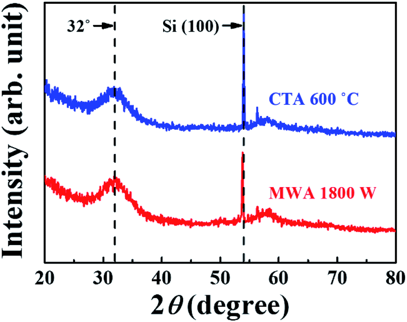
Fig. 11 illustrates the XRD patterns of IGZO nanofibers for the calcination method. Except for the sharp peak due to the substrate (100) Si single crystal at 55°, no peaks due to the IGZO crystal were found in both the CTA and MWA calcination processes. Instead, only an amorphous-like IGZO broad peak appeared at 32°. These results suggest that IGZO nanofibers exist in an amorphous state regardless of the calcination process. Thus, this result implies that impurities dominate the device performance, not crystallinity or grain size. In addition, the calcination is an important process for determining device performance because it has an absolute influence on these impurities.
 |
| | Fig. 11 XRD patterns of CTA-calcined and MWA-calcined IGZO nanofibers. | |
Conclusions
We fabricated IGZO nanofiber FETs using electrospinning and introduced an MWA technique for calcination. The MWA allowed rapid calcination of the electrospun IGZO nanofibers and dramatically reduced the thermal budget delivered to the device. The diameter of the MWA-calcined IGZO nanofibers was found to be 200 nm, which is lower than that of the CTA-calcined IGZO nanofibers, suggesting that MWA is more effective for PVP removal and IGZO nanofiber calcination. In particular, we improved the mechanical performance with excellent adhesion and the optical characteristics with high transmittance through MWA calcination. Furthermore, MWA calcination significantly improved the electrical properties, such as VTH, Nch, μFE, SS, ION/IOFF, Dit, and NSS, and enhanced the reliability under PBTS and NBTS compared with the CTA process. In conclusion, the low thermal-budget MWA technique with high energy transfer efficiency can be actively applied to IGZO nanofibers as an effective calcination method.
Conflicts of interest
There are no conflicts to declare.
Acknowledgements
This work was supported by the National Research Foundation of Korea (NRF) grant funded by the Korea government (MSIT) (No. 2020R1A2C1007586). This research was funded and conducted under the Competency Development Program for Industry Specialists of the Korean Ministry of Trade, Industry and Energy (MOTIE), operated by Korea Institute for Advancement of Technology (KIAT) (No. P0002397, HRD program for Industrial Convergence of Wearable Smart Devices).
Notes and references
- Z. Y. Yuan and B. L. Su, Colloids Surf., A, 2004, 241, 173 CrossRef CAS.
- H. Hou and D. H. Reneker, Adv. Mater., 2004, 16, 69 CrossRef CAS.
- E. P. S. Tan and C. T. Lim, Compos. Sci. Technol., 2006, 66, 1102 CrossRef CAS.
- Y. Li, X. Y. Yang, Y. Feng, Z. Y. Yuan and B. L. Su, Crit. Rev. Solid State Mater. Sci., 2012, 37, 1 CrossRef.
- D. Li and Y. Xia, Nano Lett., 2003, 3, 555 CrossRef CAS.
- H. Jiang, J. Ma and C. Li, Adv. Mater., 2012, 24, 4197 CrossRef CAS.
- N. G. Cho and I. D. Kim, Sens. Actuators, B, 2011, 160, 499 CrossRef CAS.
- D. Li, Y. Wang and Y. Xia, Nano Lett., 2003, 3, 1167 CrossRef CAS.
- S. S. Mali, H. Kim, W. Y. Jang, H. S. Park, P. S. Patil and C. K. Hong, ACS Sustainable Chem. Eng., 2013, 1, 1207 CrossRef CAS.
- A. Frenot and I. S. Chronakis, Curr. Opin. Colloid Interface Sci., 2003, 8, 64 CrossRef CAS.
- N. Bhattarai, D. Edmondson, O. Veiseh, F. A. Matsen and M. Zhang, Biomaterials, 2005, 26, 6176 CrossRef CAS.
- H. Wu, L. Hu, M. W. Rowell, D. Kong, J. J. Cha, J. R. McDonough, J. Zhu, Y. Yang, M. D. McGehee and Y. Cui, Nano Lett., 2010, 10, 4242 CrossRef CAS.
- N. Bhardwaj and S. C. Kundu, Biotechnol. Adv., 2010, 28, 325 CrossRef CAS.
- Y. Meng, G. Liu, A. Liu, Z. Guo, W. Sun and F. Shan, ACS Appl. Mater. Interfaces, 2017, 9, 10805 CrossRef CAS.
- F. Wang, L. Song, H. Zhang, Y. Meng, L. Luo, Y. Xi, L. Liu, N. Han, Z. Yang, J. Tang and F. Shan, Adv. Electron. Mater., 2018, 4, 1700336 CrossRef.
- A. Liu, Y. Meng, H. Zhu, Y. Y. Noh, G. Liu and F. Shan, ACS Appl. Mater. Interfaces, 2017, 10, 25841 CrossRef.
- V. Thavasi, G. Singh and S. Ramakrishna, Energy Environ. Sci., 2008, 1, 205 RSC.
- N. A. Barakat, B. Kim and H. Y. Kim, J. Phys. Chem. C, 2008, 113, 531 CrossRef.
- C. J. Ko, Y. K. Lin and F. C. Chen, Adv. Mater., 2007, 19, 3520 CrossRef CAS.
- L. F. Teng, P. T. Liu, Y. J. Lo and Y. J. Lee, Appl. Phys. Lett., 2012, 101, 132901 CrossRef.
- J. Y. Pyo and W. J. Cho, J. Korean Phys. Soc., 2018, 73, 978 CrossRef CAS.
- L. Shao, K. Nomura, T. Kamiya and H. Hosono, Electrochem. Solid-State Lett., 2011, 14, H197 CrossRef CAS.
- C. S. Fuh, P. T. Liu, W. H. Huang and S. M. Sze, IEEE Electron Device Lett., 2014, 35, 1103 CAS.
- Y. H. Lin, H. Faber, S. Rossbauer and T. D. Anthopoulos, Appl. Phys. Lett., 2013, 102, 193516 CrossRef.
- D. A. Koutsouras, N. A. Hastas, D. H. Tassis, C. A. Dimitriadis, P. Frigeri, S. Franchi, E. Gombia and R. Mosca, J. Appl. Phys., 2005, 97, 064506 CrossRef.
- W. T. Chen, S. Y. Lo, S. C. Kao, H. W. Zan, C. C. Tsai, J. H. Lin, C. H. Fang and C. C. Lee, IEEE Electron Device Lett., 2011, 32, 1552 CAS.
- K. Ghaffarzadeh, A. Nathan, J. Robertson, S. Kim, S. Jeon, C. Kim, U. I. Chung and J. H. Lee, Appl. Phys. Lett., 2010, 97, 113504 CrossRef.
- C. Avis and J. Jang, Electrochem. Solid-State Lett., 2011, 14, J9 CrossRef CAS.
- J. K. Jeong, H. Won Yang, J. H. Jeong, Y. G. Mo and H. D. Kim, Appl. Phys. Lett., 2008, 93, 123508 CrossRef.
- K. W. Jo and W. J. Cho, Appl. Phys. Lett., 2014, 105, 213505 CrossRef.
- W. G. Kim, Y. J. Tak, B. Du Ahn, T. S. Jung, K. B. Chung and H. J. Kim, Sci. Rep., 2016, 6, 23039 CrossRef CAS.
- H. Cheong, S. Ogura, H. Ushijima, M. Yoshida, N. Fukuda and S. Uemura, AIP Adv., 2015, 5, 067127 CrossRef.
Footnote |
| † Electronic supplementary information (ESI) available. See DOI: 10.1039/d0ra04963h |
|
| This journal is © The Royal Society of Chemistry 2020 |
Click here to see how this site uses Cookies. View our privacy policy here. 
 Open Access Article
 This Open Access Article is licensed under a Creative Commons Attribution-Non Commercial 3.0 Unported Licence
 and
Won-Ju Cho*
and
Won-Ju Cho*