
 Open Access Article
 This Open Access Article is licensed under a Creative Commons Attribution-Non Commercial 3.0 Unported Licence
High-performance near-infrared Schottky-photodetector based graphene/In2S3 van der Waals heterostructures†
Long Chen,
Zhenghan Li and
Chaoyi Yan *
*
State Key Laboratory of Electronic Thin Films and Integrated Devices, University of Electronic Science and Technology of China, Chengdu 610054, China. E-mail: cyan@uestc.edu.cn
First published on 22nd June 2020
Abstract
Two-dimensional (2D) β-In2S3 is a natural defective n-type semiconductor attracting considerable interest for its excellent photoelectronic performance. However, β-In2S3 based photodetectors exhibited a weak near-infrared photoresponse compared to visible wavelength in past reports. In this work, high-quality 2D β-In2S3 nanosheets were prepared by a space-confined chemical vapor deposition (CVD) method. Graphene/In2S3 van der Waals heterostructures were constructed to realize an enhanced near-infrared photodetection performance by a series of transfer processes. The photodetectors based on graphene/In2S3 van der Waals heterostructures through junction carrier separation exhibited a better infrared performance of high photoresponsivity (Rlight) of 0.49 mA W−1, external quantum efficiency (EQE) of 0.07%, and detectivity (D*) of 3.05 × 10⁷ jones using an 808 nm laser.
Introduction
Since the discovery of graphene, two-dimensional (2D) materials have demonstrated extremely impressive mechanical, electronic and optoelectronic properties of mechanical flexibility, adjustable bandgap and strong light–matter interactions.1–13 With the booming development of the 2D metal sulfides, multiphase In2S3 has attracted extensive attention and been used for high-performance applications in photodetectors, phase change memory devices and catalysis.14–17 There are three main crystalline structures of α-In2S3, β-In2S3, and γ-In2S3 which have been reported.14 In particular, β-In2S3 shows a distinguished performance in different devices like photodetectors, FETs, phase-change memory devices and P–N diodes.18–20 Their excellent properties of high photosensitivity and absorption coefficient make them most promising candidates for electronic and optoelectronic applications. Although β-In2S3 have a visible bandgap from 1.9 eV to 2.3 eV, CVD-grown β-In2S3 show detection capabilities from visible light to near-infrared light due to natural defect in past reports.14 However, the near-infrared light response performance of β-In2S3 is very weak compared with the visible band. Therefore, graphene/In2S3 van der Waals heterostructures21–23 were constructed by a series of transfer process to enhance the near-infrared photoelectric detection performance. The photodetectors based on graphene/In2S3 van der Waals heterostructures showed excellent performance with a high Rlight of 0.49 mA W−1, EQE of 0.07%, and D* of 3.05 × 10⁷ jones.Results and discussion
High-quality ultrathin β-In2S3 nanosheets obtained through a space-confined chemical vapor deposition (CVD) (detail in the “Experimental”) method. Fig. 1a–c show the bright field and dark field optical images of the as-grown ultrathin triangle 2D β-In2S3 nanosheets growing on mica substrate with different confined distance (d) of 35, 20 and 10 μm, respectively. When d is 20 μm, the edge size of triangular β-In2S3 nanosheets synthesized can be up to 40 μm with an atomically flat surface and a thin thickness of about 1.5 nm shown in the corresponding atomic force microscope (AFM) image (the inset of Fig. 1b). With the decreasing of d, the thickness of β-In2S3 can decrease to 1.1 nm with a regular triangular shape as shown in Fig. 1c. The confined distance dependence of In2S3 sheets thickness and size is shown in Fig. S1.†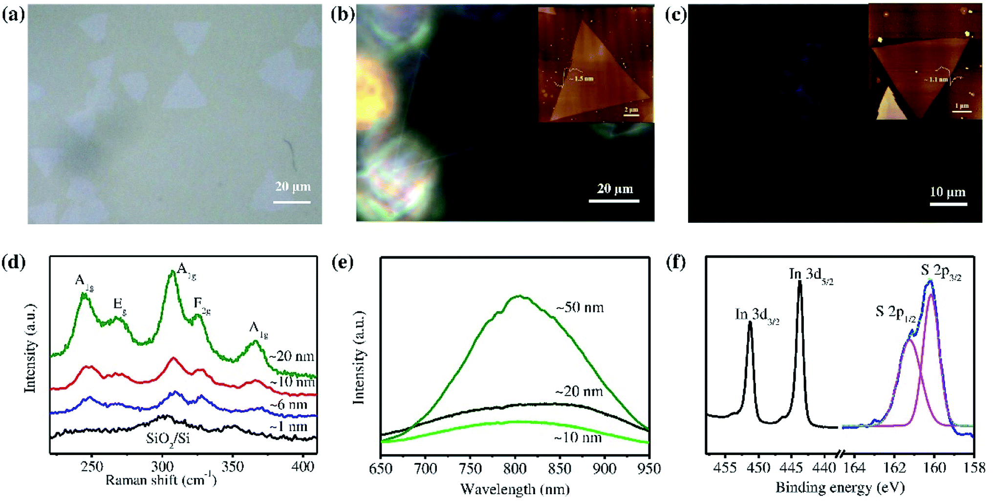 | ||
| Fig. 1 Optical images of typical as-synthesized β-In2S3 nanosheets under different confined space (d): (a) d = 35 μm. (b) d = 20 μm, the inset is the corresponding AFM image. (c) d = 10 μm, the inset is the corresponding AFM image. (d) Raman spectrum of β-In2S3 sheets with different thickness of 1, 6, 10, and 20 nm. (e) The PL spectrum of β-In2S3 sheets with different thickness of 10, 20, and 50 nm. (f) XPS spectrum of as-synthesized β-In2S3 sheets. | ||
In order to further research more characteristics of β-In2S3, Raman spectrum was used to study the vibrational mode of β-In2S3. Fig. 1d show the Raman spectrum of as-grown β-In2S3 nanosheets with different thickness. Five characteristic peaks located at 246 cm−1, 270 cm−1, 310 cm−1,328 cm−1 and 369 cm−1 of β-In2S3 nanosheets were excited by 532 nm laser, which is consistent with previous reports of β-In2S3.14 Among five peaks, the peak of 246 cm−1, 310 cm−1 and 369 cm−1 belong to the A1g vibration mode of β-In2S3, namely the out-of-plane vibration mode. The peak of 270 cm−1 belongs to the Eg vibration mode, namely the in-plane vibration mode, and the peak of 328 cm−1 belongs to the Fg vibration mode. As the thickness of 2D β-In2S3 nanosheet decreases, the strength of all peaks decreases, but the peak position of each characteristic peak does not change. When the thickness of the sample was reduced to 1 nm, there are almost no characteristic peaks of β-In2S3 due to the greatly reduced scattering center, which is similar to other 2D III–VI group materials such as InSe,24 GaSe25 and GaTe.26 Fig. 1d shows the PL spectrum of β-In2S3 nanosheets with different thickness obtained under the irradiation of incident light with a wavelength of 532 nm. In the wavelength range of 700–900 nm, β-In2S3 nanosheets have a wide emission spectrum, which is derived from the defect transition (Ed) generated by the recombination of the sample's intrinsic sulphur (S) vacancy and In vacancy. The luminescence intensity generated by defects increases with the increase of sample thickness, because the concentration of intrinsic defects in samples increases with the increase of thickness. However, due to quenching effect, PL spectrum cannot show information of intrinsic band gap (Eg) of β-In2S3. Fig. 1e shows the X-ray photoelectron spectroscopy (XPS) spectra of In3d and S2p. It is found that the peak of In3d are located in the 443.7 eV (In3d5/2) and 451.3 eV (In3d3/2) and the peak of the S2p in 160.3 eV (S2p3/2) and 161.5 eV (S2p1/2). The results of the XPS were consistent with the previous β-In2S3 XPS results.14 Full XPS spectrum as shown in Fig. S2† demonstrated the as-grown β-In2S3 nanosheets obtained by the space-confined CVD method have high chemical purity.
In order to identify the crystal structure of 2D β-In2S3, transmission electron microscope (TEM) was used to analyse the transferred β-In2S3 on the Cu grid. Fig. 2a show the low-magnification TEM image of a typical triangular β-In2S3 sheet. It can be seen that the surface of the sample is clean and free of impurities. In the HRTEM image of β-In2S3 nanosheet, clear lattice diffraction spots show good crystallinity of β-In2S3 (shown in Fig. 2b). The spacing of 0.38 nm along the parallel line can be corresponds to the (220) crystal plane of β-In2S3. And the corresponding the fast Fourier transform (FFT) was shown in the inset of Fig. 2b. X-ray energy dispersive spectrometer (EDS) was used to analyse the distribution of In and S elements of In2S3 nanosheets (Fig. 2c and d). In elements and S elements are evenly distributed on the entire triangle β-In2S3 sample. It has been proved that the high crystallization quality and clean surface β-In2S3 nanocrystals have been prepared by the CVD method.
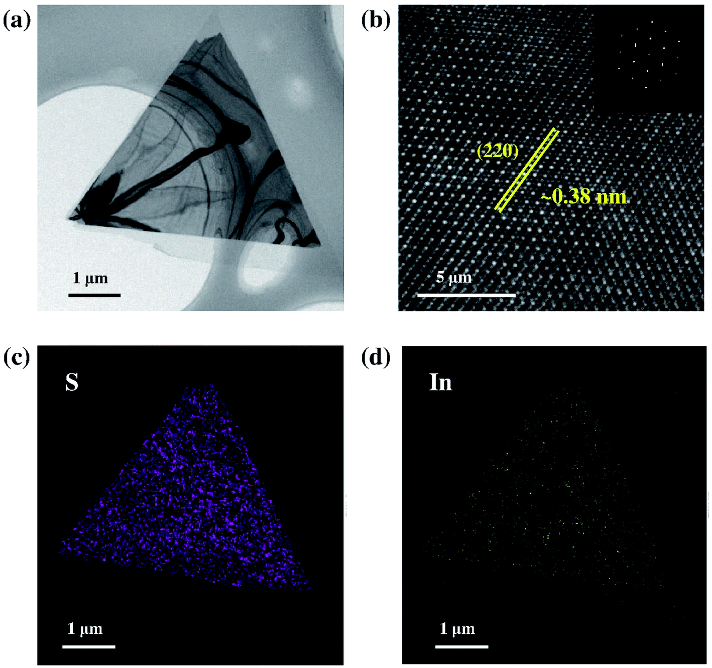 | ||
| Fig. 2 TEM characterizations of the β-In2S3 nanosheet. (a) The low-magnification TEM image of a typical triangular β-In2S3 sheet. (b) HRTEM image of β-In2S3 sheet, the inset shows the corresponding the fast Fourier transform. (c) In and (d) S elemental mapping of the β-In2S3 nanosheet in (a). | ||
Although β-In2S3 has a direct bandgap from 1.9 eV to 2.3 eV belong to visible wavelength, β-In2S3-based photodetectors have a broad photoresponse range from visible to near-infrared wavelength due to the unique defective structure. However, β-In2S3 based photodetectors have a weaker light detection performance under the infrared radiation compared to these under the visible wavelength radiation in the past report.14 Graphene/In2S3-based Schottky-photodetectors constructed to enhance infrared photoelectric detection performance. Fig. 3a shows the current–voltage curve (I–V curve) of β-In2S3-based photodetectors under the light wavelength of 808 nm and dark. Typical optical image of β-In2S3 based on photodetectors is shown in the inset of Fig. 3a. The dark current of β-In2S3 based on photodetectors is about 1.76 pA and the on/off radio is only of 1.54. Fig. 3b shows the current–time (I–T) curve under the incident light irradiation with different light power density when Vbias = 1 V. The photocurrent can be expressed by a power law of Iph ∼ Pθ. The θ value of β-In2S3 based on photodetectors is about 0.61 (shown in Fig. 3c), which indicates that the near-infrared light response of β-In2S3 nanosheets to 808 nm wavelength is mainly derived from the defect state. The defect state in the material is easier to capture the photocarrier with the increasing of optical power density, resulting in the saturation of devices' photocurrent and the nonlinearly curve shown in Fig. 3c.14,27–32 Fig. 3d shows the stability of the β-In2S3 based photodetectors with periodic switching tests. Obviously, the photocurrent and dark current of β-In2S3 based photodetectors have a large noise.
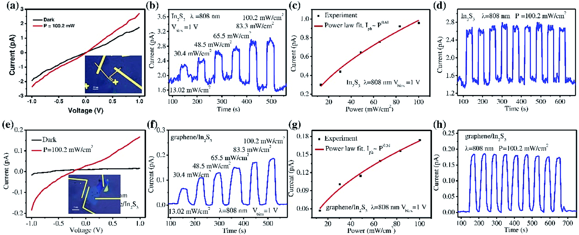 | ||
| Fig. 3 Optoelectronic properties of β-In2S3-based and graphene/In2S3-based photodetectors: the current–voltage curve (I–V curve) under a laser radiation of 808 nm and dark (a) β-In2S3-based photodetector and (e) graphene/In2S3-based photodetector. The inset is typical optical image of β-In2S3-based and graphene/In2S3-based photodetectors, respectively. The current–time (I–T) curve under the incident light irradiation with different light power density, Vbias = 1 V: (b) β-In2S3-based photodetector and (f) graphene/In2S3-based photodetector. Photocurrent as a function of illumination power: (c) β-In2S3-based photodetector and (g) graphene/In2S3-based photodetector. Time-resolved photoresponse of photodetectors at a bias voltage of 1 V and illumination power of 100.2 mW cm−2: (d) β-In2S3-based photodetector and (h) graphene/In2S3-based photodetector. | ||
Correspondingly, Fig. 3e is the I–V curve of heterojunction optoelectronic device irradiated by incident light at 808 nm wavelength and dark. The apparent difference is that the heterojunction device shows a large switching ratio of 11.16 and a smaller dark current of 0.015 pA at 1 V. The Raman spectrum with two kinds of material characteristic peak demonstrates that the vertical structure was constructed between the low layer graphene and β-In2S3 (Fig. S3†). Fig. 3f shows the light response curve under the irradiation of incident light with different light power density and the corresponding fitting value θ was 0.51 (Fig. 3g). The sub-linear relationship between the photocurrent and the optical power density curve may be caused by the intrinsic defects of β-In2S3 and the adsorption state at the interface with graphene and substrate. For stability testing, heterojunction devices exhibit more stable switching and image noise is much lower than that of individual devices (Fig. 3h).
In order to show the performance of heterogeneous junction device is improved compering with that of the β-In2S3 based device, the key parameters of photodetector including Rlight, EQE, and D* were calculated and defined as follows:
| Rlight = Ilight − Idark/PlightS |
| EQE = hcRlight/eλ |
| D* = RlightS1/2/(2eIdark)1/2 |
The PL spectrum of graphene/In2S3 heterojunction is tested to study the mechanism of improving the infrared detection performance (Fig. 4a). It can be seen that the PL spectrum of graphene/In2S3 heterojunction is similar to that of β-In2S3, but the strength of PL peak is significantly weakened and the quenching effect appears. The PL mapping as shown in Fig. 4b further illustrates this point. This phenomenon can be attributed that the carrier recombination is avoided due to the photogenerated carriers were effectively separated at the interface of β-In2S3 and graphene and flows into graphene and β-In2S3 at the junction area, respectively, which is shown in Fig. 4c. For photodetectors, due to the high light transmittance of graphene, the light absorption of heterojunction mainly comes from β-In2S3. When photons are absorbed by the heterojunction, the electrons separate from the holes, which are captured by β-In2S3, and the electrons flow to graphene. The captured holes in β-In2S3 can act as local grids in the graphene channel to regulate its charge transfer. The difference of electron–hole transport time and the increase of the lifetime of the photocarrier is the reason why the heterojunction has a great response to the near-infrared light.
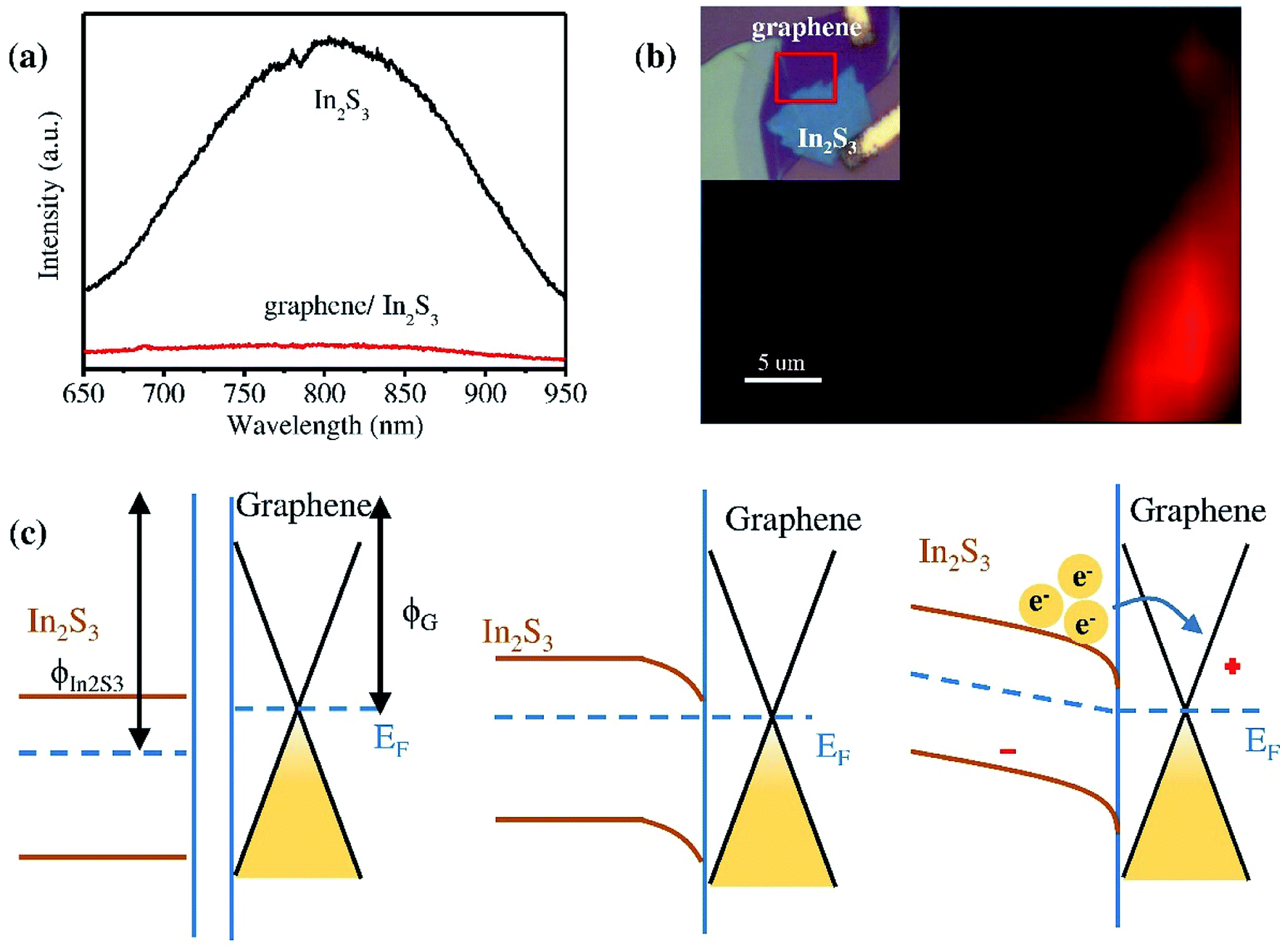 | ||
| Fig. 4 (a) PL spectrum of the β-In2S3 sheet and graphene/In2S3 heterojunction. (b) PL mapping of graphene/In2S3 heterojunction, the inset shows the optical image of graphene/In2S3 heterojunction. (c) Schematic diagram of electronics band structure of graphene/In2S3 heterojunction. | ||
Experimental
CVD growth of β-In2S3
Space-confined CVD is used for synthesis of 2D ultrathin β-In2S3 nanosheets. The quartz tube with the dual-temperature zone tubular furnace was used to support the stable growing environment as shown in Fig. S4.† Before growing process, 15 mg InI and 0.1 g S powder as precursors were placed in two Al2O3 porcelain boats, which were placed at the first heating zone of the upstream of tube furnace with an apart distant of 9 cm. Fresh fluorophlogopite mica sheets were selected as the growth substrate due to highly passivated and flat surface with extremely low migration energy of adsorbed atoms. “Face to face” superimposed mica sheets were placed on the center of heating zone 2. Before the reaction starts, the inside of the quartz tube is pumped into a vacuum. And then, the high-purity argon is used to expel the air in the quartz tube. This process was called “washing” process. After “washing” process, 60 sccm of high-purity argon gas was injected at a standard atmospheric pressure as the reaction carrier gas. The heating zone 1 heated up to 680 °C in 44 min and was kept for 10 min, while the heating zone 2 heated up to 420 °C in 42 min and was kept for 14 min. After heating zone 1 heats up to 680 °C and maintains for two minutes, push the upstream InI and S powder into the insulation zone of heating zone 1. After the reaction, the system will be cooled naturally to room temperature.Device fabrication
As-grown β-In2S3 were transferred from mica to Si substrates by standard wet transfer process. PMMA is spun onto the mica substrate to protect β-In2S3 samples at 3500 rad s−1 in 60 s. Then, the surface tension of water is used to peel the organic film off the mica substrate. After that, remove the organic film from the water to a silicon substrate. The silicon substrates with organic film were heated at 135 °C for 15 minutes to steam the water and stick to the film. Then, organic film was removed by acetone solution. The construction of heterogeneous structures requires a mechanical transfer process with polyvinyl alcohol (PVA) and polydimethylsiloxane (PDMS). Firstly, the PVA/PDMS/glass slide was pasted onto the target low-layer graphene sample and heated at 55 °C for 3 minutes to peel the graphene from the silicon substrate. After that, the graphene/PVA/PDMS/glass slide was pasted onto the target β-In2S3 sample and heated at 70 °C until the PDMS can separated from PVA. After cooling to room temperature, the sample was immersed in deionized water to remove PVA.The photodetectors based on transferred β-In2S3 and graphene/In2S3 junction were fabricated by standard electron beam lithography (EBL) process. Patterning PMMA films were fabricated by EBL and the Cr/Au electrodes (10 nm/50 nm) were evaporated by thermal evaporation methods. Acetone was eventually used to remove excess photoresist and gold attached to photoresist.
Characterizations
The β-In2S3 nanosheets and graphene/In2S3 junctions were characterized by the optical microscope (BX51, OLMPUS). The thickness and morphology of In2S3 and junctions are measured by the atomic force microscope (AFM, Demension icon, Bruker). A confocal Raman/PL system (Alpha 300RS+, WITec) is used to characterized the Raman and PL spectra of In2S3 nanosheets, graphene and junctions at room temperature with a 532 nm laser. X-ray photoelectron spectroscopy (XPS, Axis Supra, Shimadzu) is adopted to analyse the electronic structure of In2S3 sheets. The transmission electron microscope (TEM, Tecnai G2 F20 S-Twin TMP, FEI) equipped with an X-ray energy dispersive spectrometer (EDS) is used to characterize the crystal structure of In2S3. Photoelectric properties of devices based on In2S3 and graphene/In2S3 junction are measured by a characterization system combined with semiconductor testing instrument (4200, Keithley), a probe station (CRX-6.5K, Lake Shore) and a laser source with adjustable wavelength of 532, 808 and 1550 nm.Conclusions
In summary, we conducted a space-confined CVD method for the controlled synthesis of ultrathin 2D β-In2S3 flakes. Furthermore, the graphene/In2S3 heterogeneous structures are implemented through a series of transfer methods. High infrared detection was realized with an excellent Rlight of 0.49 mA W−1, EQE of 0.07%, and D* of 3.05 × 10⁷ by junction carrier separation. Such a good detection performance based on 2D graphene/In2S3 opens up opportunities for the emerging metal sulfide in future application of electronics and optoelectronics.Conflicts of interest
There are no conflicts to declare.Notes and references
- C. Gong, Y. Zhang, W. Chen, J. Chu, T. Lei, J. Pu, L. Dai, C. Wu, Y. Cheng, T. Zhai, L. Li and J. Xiong, Adv. Sci., 2017, 4, 1700231 CrossRef PubMed.
- A. Raja, L. Waldecker, J. Zipfel, Y. Cho, S. Brem, J. Ziegler, M. Kulig, T. Taniguchi, K. Watanable, E. Malic, T. Heinz, T. Berkelbach and A. Chernikov, Nat. Nanotechnol., 2019, 14, 832–837 CrossRef CAS PubMed.
- M. Wang, S. Cai, C. Pan, C. Wang, X. Lian, Y. Zhuo, K. Xu, T. Cao, X. Pan, B. Wang, S. Liang, J. Yang, P. Wang and F. Miao, Nat. Electron., 2018, 1, 130 CrossRef CAS.
- L. Li, W. Han, L. Pi, P. Niu, J. Han, C. Wang, B. Su, H. Li, J. Xiong, Y. Bando and T. Zhai, InfoMat, 2019, 1, 54 CrossRef.
- J. Kim, S. Baik, S. Ryu, Y. Sohn, S. Park, B. Park, J. Denlinger, Y. Yi, H. Choi and K. Kim, Science, 2015, 6249, 723 CrossRef PubMed.
- A. Splendiani, L. Sun, Y. Zhang, T. Li, J. Kim, C. Chim, G. Galli and F. Wang, Nano Lett., 2010, 10, 1271 CrossRef CAS PubMed.
- O. Lopez-Sanchez, D. Lembke, M. Kayci, A. Radenovic and A. Kis, Nat. Nanotechnol., 2013, 8, 497 CrossRef CAS PubMed.
- H. Santos, A. Ayuela, L. Chico and E. Artacho, Phys. Rev. B, 2012, 85, 245430 CrossRef.
- T. Hung, A. Rustagi, S. Zhang, P. Upadhyaya and Z. Chen, InfoMat DOI:10.1002/inf2.12095.
- T. Alonso-Lanza, A. Ayuela and F. Aguilera-Granja, Phys. Chem. Chem. Phys., 2016, 18, 21913 RSC.
- A. Ayuela Fernández, W. Jaskólski, H. Santos Expósito and L. Chico, New J. Phys., 2014, 16, 083018 CrossRef.
- C. W. Tan, S. P. Xu, Z. J. Tan, L. Z. Sun, J. X. Wu, T. R. Li and H. L. Peng, InfoMat, 2019, 1, 54 CrossRef.
- C. Gong, Y. Zhang, W. Chen, J. Chu, T. Lei, J. Pu, L. Dai, C. Wu, Y. Cheng, T. Zhai, L. Li and J. Xiong, Adv. Sci., 2017, 4, 1700231 CrossRef PubMed.
- W. Huang, L. Gan, H. Yang, N. Zhou, R. Wang, W. Wu, H. Li, Y. Ma, H. Zeng and T. Zhai, Adv. Funct. Mater., 2017, 27, 1702448 CrossRef.
- X. Xie and G. Shen, Nanoscale, 2015, 7, 5046 RSC.
- R. Sharma, Y. Chouryal, S. Chaudhari, J. Saravanakumar, S. Dey and P. Ghosh, ACS Appl. Mater. Interfaces, 2017, 9, 11651 CrossRef CAS.
- Y. Gao, S. Zhang, X. Bu and Y. Tian, Catal. Today, 2019, 1, 271 CrossRef.
- R. H. Bube and W. H. Mccarroll, J. Phys. Chem. Solids, 1959, 4, 333 CrossRef.
- L. Bhira, H. Essaidi, S. Belgacem, G. Couturier, J. Salardenne, N. Barreaux and J. C. Bernede, Phys. Status Solidi A, 2000, 2, 427 CrossRef.
- R. Sumi, A. Warrier and C. Vijayan, J. Phys. D: Appl. Phys., 2014, 10, 105103 CrossRef.
- Y. Liu, N. O. Weiss, X. Duan, H. Cheng, Y. Huang and X. Duan, Nat. Rev. Mater., 2016, 1, 16042 CrossRef CAS.
- J. Lu, A. Wei, Y. Zhao, L. Tao, Y. Yang, Z. Zheng, H. Wang, D. Luo, J. Liu, L. Tao, H. Li, J. Li and J. Xu, ACS Photonics, 2018, 5, 4912 CrossRef CAS.
- G. Rao, X. Wang, Y. Wang, P. Wangyang, C. Yan, J. Chu, L. Xue, C. Gong, J. Huang, J. Xiong and Y. Li, InfoMat, 2019, 1, 272 CrossRef.
- X. Yuan, L. Tang, S. Liu, P. Wang, Z. Chen, C. Zhang, Y. Liu, W. Wang, Y. Zou, C. Liu, N. Guo, J. Zou, P. Zhou, W. Hu and F. Xiu, Nano Lett., 2015, 5, 3571 CrossRef PubMed.
- O. Makkawi, Y. Qiu, W. Feng and A. Ping, J. Nanosci. Nanotechnol., 2016, 9, 9813 CrossRef.
- Z. Yang, W. Jie, C.-H. Mak, S. Lin, H. Lin, X. Yang, F. Yan, S. Lau and J. Hao, ACS Nano, 2017, 4, 4225 CrossRef PubMed.
- P. Hu, Z. Wen, L. Wang, P. Tan and K. Xiao, ACS Nano, 2012, 6, 5988 CrossRef CAS PubMed.
- E. Liu, M. Long, J. Zeng, W. Luo, Y. Wang, Y. Pan, W. Zhou, B. Wang, W. Hu and Z. Ni, Adv. Funct. Mater., 2016, 26, 1938 CrossRef CAS.
- B. Jin, P. Huang, Q. Zhang, X. Zhou, X. Zhang, L. Li, J. Su, H. Li and T. Zhai, Adv. Funct. Mater., 2018, 28, 1800181 CrossRef.
- J. Yao, Z. Zheng and G. Yang, Adv. Funct. Mater., 2017, 27, 1701823 CrossRef.
- F. Wang, T. Gao, Q. Zhang, Z. Y. Hu, B. Jin, L. Li, X. Zhou, H. Li, G. Van Tendeloo and T. Zhai, Adv. Mater., 2019, 31, 1806306 CrossRef PubMed.
- P. Hu, L. Wang, M. Yoon, J. Zhang, W. Feng, X. Wang, Z. Wen, J. C. Idrobo, Y. Miyamoto and D. B. Geohegan, Nano Lett., 2013, 13, 1649 CrossRef CAS PubMed.
Footnote |
| † Electronic supplementary information (ESI) available. See DOI: 10.1039/d0ra02033h |
| This journal is © The Royal Society of Chemistry 2020 |