
 Open Access Article
 This Open Access Article is licensed under a Creative Commons Attribution-Non Commercial 3.0 Unported Licence
Influence of the cathode microstructure on the stability of inverted planar perovskite solar cells†
Svetlana Sirotinskaya ,
Roland Schmechel and
Niels Benson*
,
Roland Schmechel and
Niels Benson*
Faculty of Engineering, Institute of Technology for Nanostructures (NST), University of Duisburg-Essen, Building BA, Bismarckstr. 81, 47057 Duisburg, Germany. E-mail: niels.benson@uni-due.de
First published on 22nd June 2020
Abstract
One of the main challenges for perovskite solar cells (PSC) is their environmental stability, as oxygen and water induced aging may result in mobile decomposition compounds, which can enhance the recombination rate and react with charge carrier extraction layers or the contact metallization. In this contribution the importance of the microstructure of the contact metallization on the environmental cell stability is investigated. For this purpose, the storage stability of inverted planar methylammonium lead iodide (MAPI)-based perovskite solar cells without encapsulation is tested, using the metals aluminum (Al), silver (Ag), gold (Au) and nickel (Ni) as representative cathode materials. For this study, scanning electron microscopy (SEM) and energy-dispersive X-ray spectroscopy (EDX) analysis of the different electrodes as well as the perovskite is correlated with PSC device current–voltage (J–V) and impedance measurements. Our findings substantiate that the metal microstructure has a significant influence on the PSC aging properties. While a strong perovskite decomposition and iodide diffusion to the contacts were detected for devices using Al, Ag or Au cathodes with a polycrystalline microstructure, these effects were strongly reduced when Ni metallization was employed, where a nanocrystalline microstructure was exhibited under the chosen process conditions.
Introduction
Organic–inorganic perovskite materials such as methylammonium lead iodide (MAPI) have attracted a lot of attention in recent years, because of their excellent performance in photovoltaic applications. Their easy deposition from solution, crystallization at low temperatures and the rapid development of obtainable power conversion efficiencies from 3%![[thin space (1/6-em)]](https://www.rsc.org/images/entities/char_2009.gif) 1 to over 25%2,3 make this material class one of the most promising modern material systems for solar cells. This high efficiency is based on perovskite properties, such as a tunable band gap,4 good absorption in the solar spectral range5 and energetically flat defect states in the band gap.6 The consequence of the latter property is a long diffusion length7 and charge carrier lifetime.8 However, perovskite-based photovoltaic devices mostly exhibit a low environmental stability due to the influence of moisture, high temperatures and light. The associated degradation processes can be classified into the following groups: (I) the corrosion of the extraction and contact layers due to the reaction with MAPI decomposition components and (II) the environment-induced MAPI decomposition itself. These processes have been intensely investigated in previous years and are suggested to be the consequence of the following mechanisms.
1 to over 25%2,3 make this material class one of the most promising modern material systems for solar cells. This high efficiency is based on perovskite properties, such as a tunable band gap,4 good absorption in the solar spectral range5 and energetically flat defect states in the band gap.6 The consequence of the latter property is a long diffusion length7 and charge carrier lifetime.8 However, perovskite-based photovoltaic devices mostly exhibit a low environmental stability due to the influence of moisture, high temperatures and light. The associated degradation processes can be classified into the following groups: (I) the corrosion of the extraction and contact layers due to the reaction with MAPI decomposition components and (II) the environment-induced MAPI decomposition itself. These processes have been intensely investigated in previous years and are suggested to be the consequence of the following mechanisms.
Under illumination and the exposure to moisture, MAPI decomposes into different mobile iodine-containing components (e.g., MAI, PbI2, CH3NH3I, HI, I2 and MAI–nI2).9–12 Such a degradation does not only impair the quality of the absorber layer, but also leads to the reaction of decomposition products with the extraction layers.13 In consequence additional energetic barriers form at the extraction layer/perovskite and electrode/extraction layer interfaces, thus degrading the electronic transport. Further, such iodine containing components can corrode the metal contacts of the photovoltaic cell, degrading their conductivity. Consequently, in order to increase device stability without changing the PSC architecture, several research groups have started to consider a modification of the contact metallization. This concept has the advantage, that it does not influence the open-circuit voltage14 when compared to an ETL or HTL modification. It was demonstrated that Ag electrodes degrade due to a chemical reaction with decomposed perovskite iodide components.15–18 A similar, yet stronger reaction is observed for Al contacts.11,19,20 A different type of degradation process is observed for Au contacts.21,22 In this case, not only an iodine diffusion to the contact interface needs to be considered, but also an Au atom diffusion into the perovskite layer. The later process leads to enhanced charge carrier recombination, which further impairs the performance of the solar cells. Another issue with the use of Au contacts is the influence a catalytic effect with methylammonium lead iodide, as reported by Kerner et al.23 This contribution suggests the Au accelerated decomposition of MAPI to hydroiodic acid (HI). Recently Shlenskaya et al. have suggested yet another degradation process associated with Au electrodes in contact with MAPI, which is based on the formation of reactive iodide melts and their interaction with Au.9,10 While the reactivity of the contact metals is the focus of most of the discussed scientific contributions, the morphology or microstructure influence of the cell top metallization has not yet been investigated. In general, separating the different degradation processes is difficult, yet required to evaluate the influence of the metal microstructure. In the following, we therefore outline a comparative degradation study of different contact materials with different chemical reactivities, allowing us to separate the influence of the contact corrosion, the metal-accelerated MAPI decomposition and the environment-induced MAPI aging. In this effort, the device structure and the testing conditions have been kept the same for all PSCs, allowing us to determine the influence of the metal microstructure on the observed degradation processes. For our investigation, we chose Al, Ag and Au as standard PSC contact materials, with inherently different reactive and morphological properties, as well as Ni as a low cost, stable material representative.
Results
The architecture of the investigated planar p–i–n PSCs and their energy level diagram is illustrated in Fig. 1(a and b). The following metal work function values were assumed: 4.6 eV (Ag), 4.2 eV (Al), 5.2 eV (Ni), 5.3 eV (Au).24 As HTL and ETL, copper iodide (CuI) and buckminsterfullerene (C60) were used. A bathocuproine (BCP) layer was used as an additional hole blocking layer together with the ETL. In order to investigate the influence of different top contact metallizations on the cell performance and stability, J–V measurements were carried out using an AM 1.5 spectrum with a power density of 100 mW cm−2. For our aging experiment, the characterization was done directly after the preparation (Fig. 1(c–f)) and in regular intervals during the next 32 days (Fig. 3). During this time frame, a sample set was stored in the dark at 20–23 °C in air (about 20–30% RH) and an additional sample set under inert nitrogen (N2) atmosphere (<0.1 ppm O2, H2O). Fig. 1(d–f) illustrates the dependency of the average solar cell power conversion efficiency (PCE), the open-circuit voltage (Voc) and the short-circuit current density (Jsc) on the metal work function. The best-achieved efficiencies are approximately 16% for devices with Al cathodes, making these devices comparable to state of the art perovskite solar cells with a similar device architecture.25,26 As the aim of this contribution is the evaluation of the top contact metallization microstructure influence on the PSC stability, no further charge transport layers were tested. As shown in Fig. 1(f), no strong correlation between Voc and the metal work function was observed. This is well in line with the results of Behrouznejad et al.,14 which were obtained using a regular n–i–p structure. For Al, Au and Ag a Voc between 0.9 V and 1 V was determined, while the Voc for Ni was clearly reduced with a value of 0.8 V. We suggest this to be the consequence of an energetic barrier resulting from a non-ohmic contact between the Ni and the BCP layer.27,28 In Fig. 2, top- and bottom-view images of the different top contact metallization solar cells are shown, after one week of testing and storage in air as well as N2. We note that all the devices were stored in the dark, in order to minimize light-induced degradation. The first degradation indication is directly visible for cells with Al and Ag contacts. The Al contact devices exhibit strong degradation after storage in air (Fig. 2(c)) and visible degradation in N2 (Fig. 2(d)), as the metal contacts become visible through the black perovskite layer. This indicates a strong Al corrosion process, making further measurement impossible. The Ag contact degradation and the associated MAPI decomposition for cells stored in air is noticeable by the yellow color of the perovskite at the contact edge of (top view) and below this contact (bottom view). Dashed red lines in Fig. 2 mark all visible degradation effects. No visible degradation for PSCs with Au and Ni electrodes is observed.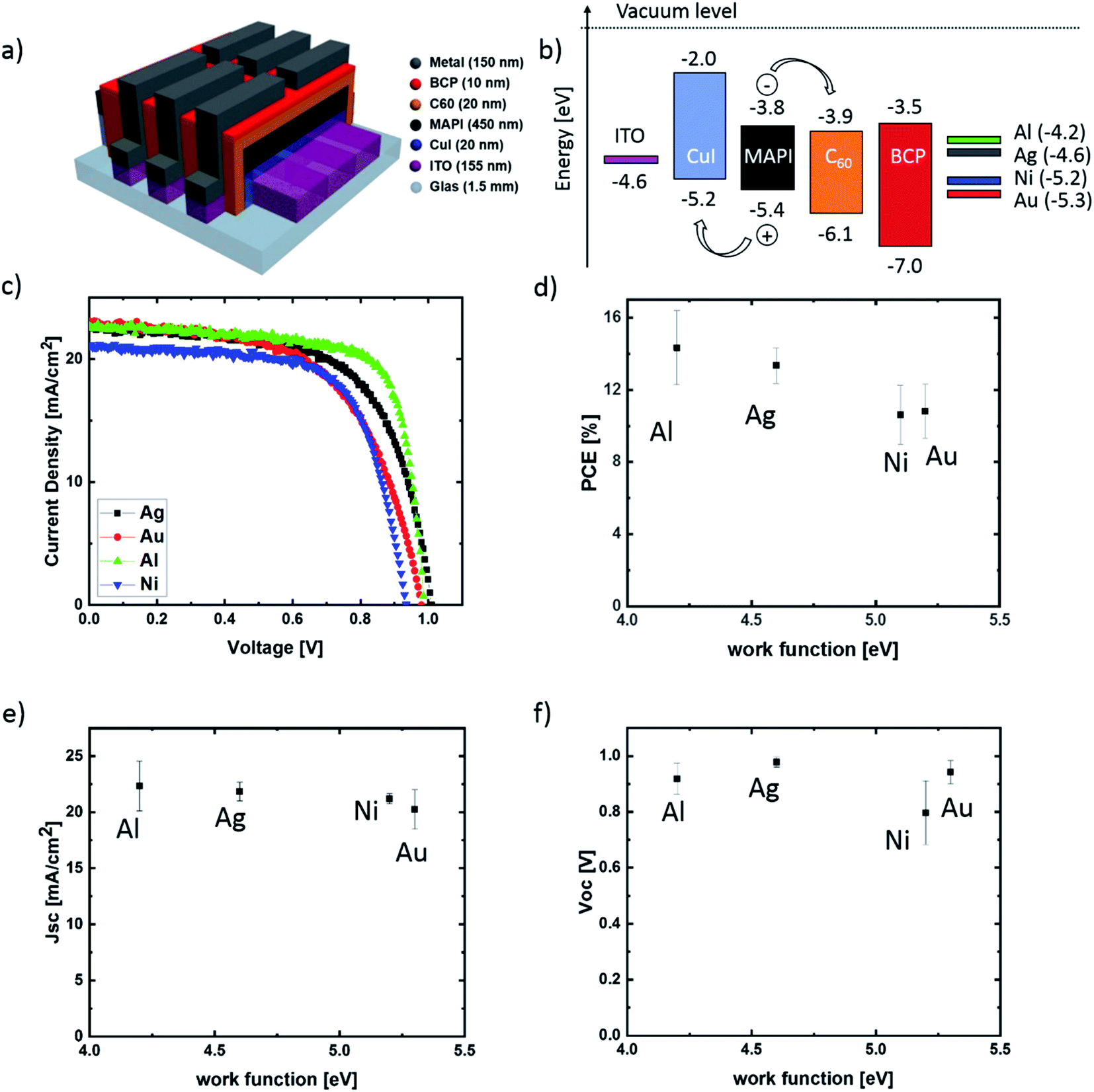 | ||
| Fig. 1 (a) Device architecture of a planar PSCs, (b) band diagram of layers in a PSC, (c) J–V characteristics of typical fresh devices with different contact materials, (d) dependency of average efficiency, (e) open-circuit voltage and (f) short-circuit current on the work function of contact metals. For each metallization 36 PSCs were tested. | ||
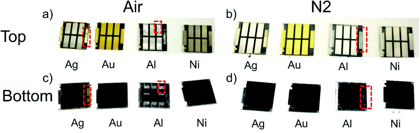 | ||
| Fig. 2 (a and b) Top, and (c and d) bottom view of solar cells after one-week storage (a and c) in the ambient and (b and d) in N2 atmosphere with Ag, Au, Al and Ni electrodes. | ||
The result of the electrical degradation evaluation for the respective atmospheric conditions over the entire time period of 32 days is illustrated in Fig. 3, for the parameters PCE, Voc, Jsc and FF. The IV characteristics exhibited only a neglectable hysteresis, and the maximum power point tracking was done manually for each measurement. Both topics are described in the ESI section.† The individual cell parameters have been normalized with respect to the initial values obtained for the as-fabricated devices (t = 0). While the solar cells with aluminum and silver contacts degrade much more rapidly in air than in nitrogen, the degradation of cells with gold electrodes is almost independent of the storage conditions. This result matches well with the optical observations discussed for Fig. 2. Remarkably, a strong improvement of approximately 50% in PCE, up to 15% absolute PCE, was obtained during the first days of testing for the devices with Ni top electrodes. More importantly, even after the controlled aging for 32 days in N2 and ambient atmosphere, the PCE does not drop below the PCE values obtained at t = 0. This indicates a very slow aging for these devices. As already discussed, the Al contact PSCs underlie the most rapid degradation, which is mainly the consequence of a drop in Jsc during the first days. For this type of cell, an efficiency decrease of 100% and 90% was obtained after two-week storage in ambient and nitrogen atmosphere. This is in line with the observed strong electrode corrosion and perovskite decomposition. The cells with Ag top contact metallization show a clear difference in their electrical degradation behavior when compared to the Al based devices, despite a visible contact corrosion. Here the cells stored for two weeks in N2 degrade only by approximately 10% in PCE, which is mainly due to a decrease in Voc, while the cells stored in ambient conditions still show a 60% degradation in PCE due to a decrease in Voc, Jsc and FF. While no visible structural degradation for PSCs with Au electrodes was observed, these devices still exhibit an electrical degradation for all J–V parameters. We found an efficiency decrease of ∼50% after one-month of storage, independent of the storage conditions. For the special case of the cells with Ni top electrodes, the gain in PCE during the first days of testing is the result of an increase in the open-circuit voltage. This is in line with the observation by Jiang et al., who observed a Voc and FF enhancement in MAPI n–i–p devices with Ni electrodes after one day of storage in a desiccator.29 We suggest this to be the result of a slow diffusion of Ni atoms into the BCP layer and the generation of transport states in the BCP band gap.27,28 Such a process may lead to a Ni/BCP interface improvement. We also speculate that the other reason for the low initial Voc and its subsequent enhancement is the consequence of BCP damage during the Ni evaporation process and a possible self-healing. As already implied above, no significant degradation in solar cell performance for MAPI devices with Ni top electrodes was observed during the 32 days of degradation testing.
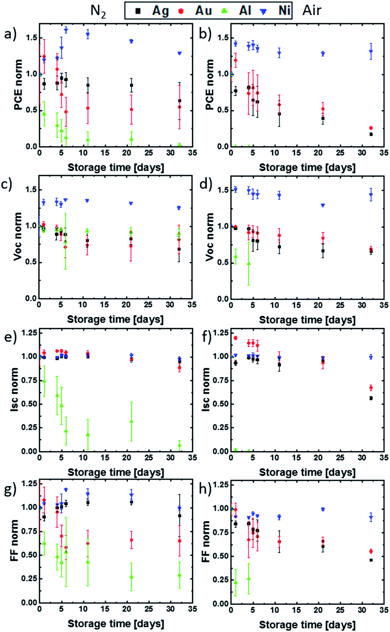 | ||
| Fig. 3 Degradation of PSCs due to the storage in ambient (a–d) and nitrogen (e–h) atmosphere. Dependence of normalized PCE (a and e), Voc (b and f), Jsc (c and g) and FF (d and h) on the storage time. | ||
In order to further investigate the observed contact corrosion, impedance spectroscopy measurements (IS) were carried out. With this method it is possible to distinguish between the influence of the perovskite bulk and the ETL/perovskite interface on the electronic PSC properties. This is the consequence of a different frequency response for different charge transport mechanisms.30 While the response of ion and deteriorated electron transport in degraded devices is measurable at low frequencies, the influence of the perovskite/ETL interface on the charge carrier transport corresponds to the high-frequency part.30 For this reason, the frequency range from 1 kHz to 1 MHz was chosen. The measurements were done under 100 mW cm−2 (AM 1.5) illumination and open-circuit condition, ensuring that the device was operated under maximum recombination conditions.31,32 Moreover, in this setting the charge carriers are accumulated at the perovskite/ETL and HTL interfaces, increasing the recombination probability at these cell boundaries.31 For the data interpretation, the two-component Voigt model is used, as outlined in the ESI.†33 In this model, the interaction between the electrode or transport layers with the perovskite thin film is represented by the semi-circle obtained between 1 MHz and 10 kHz, as shown in Fig. 4 for the different top contact metallization PSCs.14,34 Because of the assumed metal diffusion into the ETL, its small thickness and the fact that the same ETL and HTL were used for all PSCs, we assume the observed differences in the IS measurements to be the consequence of the different contact metallizations. While the change in pure metal series resistance is almost neglectable, due to the missing semi-circle shift on the Z′-axis, a significant increase in the semi-circle radius was observed. This implies a significant increase in interfacial charge-carrier recombination activity (due to interface defect state formation, etc.), which will be the main cause for the J–V characteristic change during the aging experiment. For the case of Ag electrodes, after two weeks of storage in air, the increase in semi-circle radius corresponds to a perovskite/transport layer interface resistance (Rper/TL) increase by a factor of 20, while the perovskite/TL interface capacitance (Cper/TL) remains almost unchanged. During the same time frame, Rper/TL changed by a factor of 6 and 2 for PSCs with Au and Ni electrodes. This implies a significantly slower metal/perovskite interface trap formation, when compared to cells with Ag electrodes. This observation is supported by an SEM cross-sectional analysis of the different interfaces, demonstrating a Ag/MAPI interface deterioration, whereas no morphology change was detected for degraded PSCs with Au and Ni contacts (see ESI†). The technical parameters of this analysis are outlined in the Experimental section.
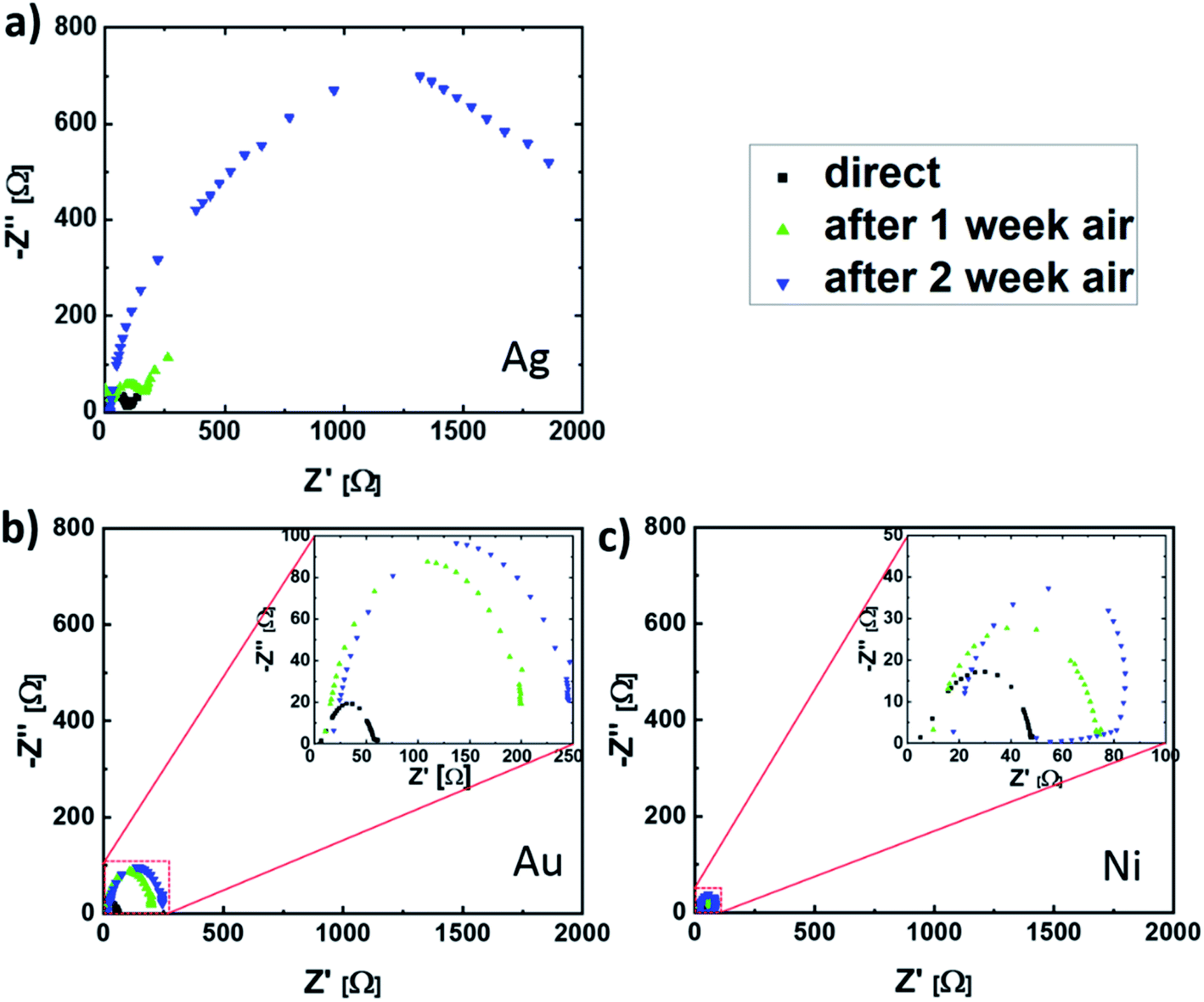 | ||
| Fig. 4 Nyquist plots for solar cells with (a) Ag, (b) Au and (c) Ni contacts directly after fabrication and after one- and two-week storage in air. | ||
At this point, we have demonstrated that the degradation of PSCs with Au and Ni contacts is not the consequence of a MAPI/ETL or MAPI/electrode reaction. We hypothesize that the observed difference in degradation is the consequence of MAPI bulk changes, which are related to the top metal microstructure, as outlined in the following.
As the device architecture is identical for all investigated PSCs, we suggest the difference in degradation to be the consequence of metal microstructure influenced water diffusion. Depending on the metal contact microstructure, moisture may diffuse into the perovskite layer, not just from the sides of the cell as suggested by Kato et al.,15 but also through the metal contact itself, which will result in enhanced water uptake. The microstructure of the evaporated Al, Ag, Au and Ni contact layers is shown in Fig. 5, using images obtained from a SEM analysis. It stands out, that Al, Ag and Au films have a clear polycrystalline structure with a broad crystallite size distribution, a rough surface and well-defined grain boundaries. In contrast, the nickel electrode consists of highly dense nanocrystallites (<10 nm) and a smooth surface. The blurred structure under the nickel film is related to the perovskite surface. The origin of this microstructure variation is the difference in melting temperature for the used metals.35–39 It is well known that thermally evaporated, as well as sputtered metal thin films have a polycrystalline morphology. Here the crystallite size is dependent on the ratio of the substrate temperature (TS)/metal melting temperature (TM). Depending on this ratio, 4 different growth regions are possible as shown in Fig. 5. Zone 1 represents a nanocrystalline metal phase, while zone T yields a transition zone between the nanocrystalline structure of zone 1 and the larger grained polycrystalline zones 2 and 3. For the case at hand, the different metallizations were deposited without any cooling at substrate temperatures of ∼350 K. This results in a TS/TM ratio of 0.37, 0.28, 0.26 and 0.20 for the respective Al, Ag, Au and Ni metallization. This means that Ni, Au and Ag will form thin films related to zone T. However, as zone T is the transition zone between zones 1 and 2, and by taking the SEM micrographs shown in Fig. 5 into account, we suggest, that the Ni thin films form more at the nanocrystalline end of the scale and exhibit undefined grain boundaries, while the Ag and Au thin films form a polycrystalline thin film with well-defined grain boundaries. As the grain boundary diffusion in metal films is usually several times larger than the lattice diffusion, the absence of clearly formed grain boundaries in the Ni thin films prevents moisture diffusion into the perovskite thin film.40,41
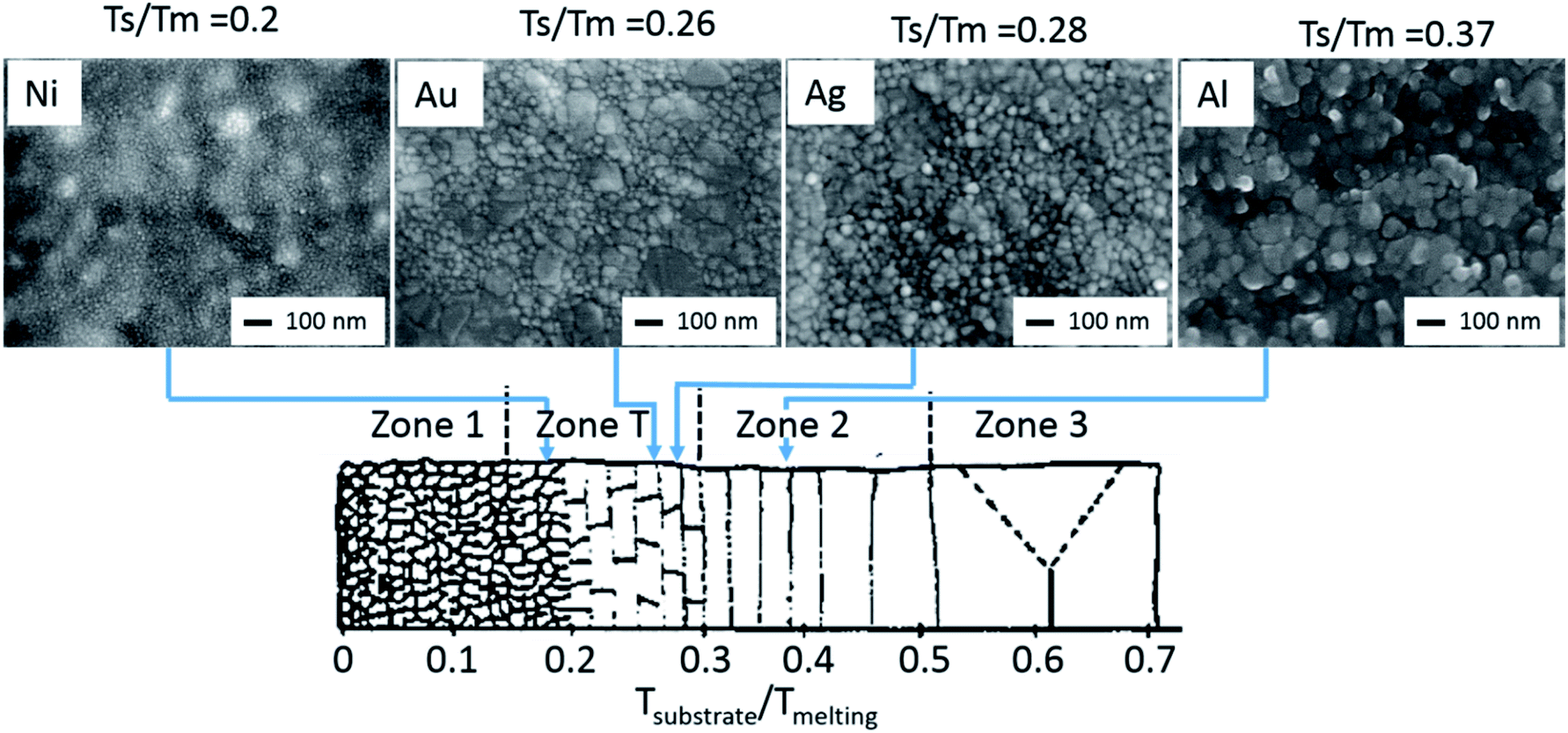 | ||
| Fig. 5 SEM top view micrographs of 100 nm thick Ni, Au, Ag and Al layers. While the Ag and Au films have a clear polycrystalline structure with a broad crystallite size distribution, rough surface and well defined grain boundaries, the nickel film consists of highly dense nanocrystallites (<10 nm) and has a smooth surface. This observation is in line with zone models, where the morphological differences are defined due to the substrate temperature (TS)/metal melting temperature (TM) ratio. Modified from ref. 36, with the permission of Elsevier. | ||
In order to verify our theory regarding the moisture diffusion dependency on the contact microstructure, cross-section EDX measurements of the two-month-old devices stored in ambient atmosphere were carried out. While the mapping measurements (see ESI†) implicate a constant perovskite composition along the cell cross-section, line scan EDX measurements were carried out to quantify the analysis (Fig. 6) further. For the measurements, an extraction voltage of 15 kV and a probe current of 10 mA was used to detect the MAPI constituents iodide and lead. Because of the high extraction voltage and large detection depth, only approximate trends and average values can be considered for this type of investigation. The result of the experiment is illustrated in Fig. 6. It is surprising to see that after two months of storage, the Pb:I ratio has degraded throughout the cell to a ratio of 1:1 for devices with Au and to a ratio of 1:1.2 for devices with Ag contacts. This stands in contrast to the result obtained for devices with Ni electrodes, where the Pb:I ratio remains 1:3 throughout the perovskite thin film, as it would be expected for an intact perovskite stoichiometry. We conclude the observed degradation in Pb:I ratio to be the consequence of the water uptake dependent perovskite decomposition into volatile iodide compounds and their diffusion out of the perovskite layer/cell. Therefore, the enhanced stability for PSCs with Ni electrodes is in line with the observed nanocrystalline microstructure of the Ni metallization.
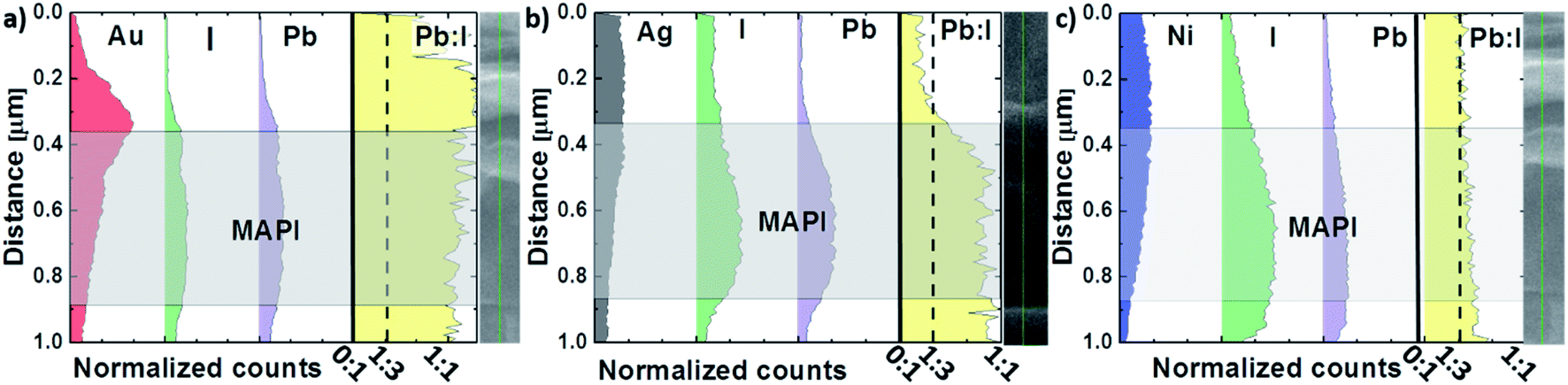 | ||
| Fig. 6 Normalized cross-section EDX line scan of degraded PSCs with (a) Au, (b) Ag and (c) Ni contacts. Iodide and lead are presented by green and purple color respectively. | ||
Interestingly, similar storage stability is reported for PSCs with a copper (Cu) top contact metallization.42,43 The TS/TM = 0.258 value is slightly lower than the value of Au (TS/TM = 0.262). Consequently, for this experiment, a similar or slightly denser Cu microstructure is expected when compared to the Ag and Au metallization microstructure discussed in this contribution. We suggest that three reasons may lead to the stability improvement of Cu-contacted PSCs. First, the metal thin film microstructure is heavily dependent on its deposition conditions, which may result in a nanocrystalline Cu microstructure and improved PSC device stability.43 Second, there are no reports regarding a catalytic effect of Cu on the MAPI decomposition, which may lead to improved PSC stability.23 Third, an oxidation of Cu to Cu2O may occur in air, which could prevent a moisture diffusion into the perovskite layer, similar to the discussed microstructure.
Conclusion
In this contribution, we demonstrate the influence of the cathode microstructure on the stability of inverted planar MAPI-based solar cells. We find that a nanocrystalline microstructure, due to its highly dense packing, has a beneficial effect on PSC stability. This improvement is related to reduced water diffusion into the solar cell. The resulting lower water uptake suppresses the moisture-related MAPI decomposition and the formation of volatile iodine containing groups. We have demonstrated this using a detailed comparative PSC degradation study using solar cells with Ni, Ag, Al and Au contacts. In our experiment, the Ni cathode is the only metallization that has the required microstructure for reduced solar cell water uptake and therefore allows for devices with impressive stability during our one month of degradation testing.Experimental
Materials
MAI (98%), DMSO (>99.9% for molecular biology), DMF (99.8% anhydrous), diethyl ether (99.9%), BCP (99.99%) and C60 (99.5%) were purchased from Sigma Aldrich. PbI2 (99.9985%) was purchased from Alfa Aesar. Acetonitrile was received from HiPerSolv CHROMANORM. CuI was synthesized using the well-known method by the mixing of water solution of copper(II) sulfate with potassium iodide. Afterward, the sediment was washed with water and dried in vacuum.Fabrication of solar cells for J–V and impedance characterization
Indium tin oxide (ITO)-coated glass sheets with a resistivity of 15 Ω sq−1 were patterned by Naranjo substrates. They were subsequently cleaned with aceton, a 3% mucasol solution, a 1:1 mix of isopropanol and acetone and finally ethanol. Directly before applying the hole transport layer, remaining organic residues were removed by an oxygen plasma treatment for 15 min at 130 °C. CuI solution was prepared by solving 10 mg of CuI powder in 1 ml Acetonitrile. Diethyl ether layer (about 30 nm) was deposited on the top of ITO substrates by spin-coating in a glovebox at 3000 rpm for 30 s. The CuI layer was then annealed for 10 min at 100 °C.25 Afterward, the substrates were transferred out from the glovebox and the perovskite layer was deposited. We used the anti-solving method published by Park et al. to get a hole-free perovskite layer.44,45 Perovskite solution was prepared by dissolving 1 mmol of PbI2 (461 mg) and MAI (156 mg) in 530 mg of DMF, in which 1 mmol of dimethyl sulfoxide (DMSO) (78 mg) was added. The solution was filtered using a syringe filter with a pore size of 0.45 μm. The 20 μl of the solution was applied on the top of the CuI layer and then spin-coated at 4000 rpm for 25 s. After 12 s spin-coating, 0.28 ml of diethyl ether was added. The adduct film was converted to the polycrystalline MAPI layer by the annealing at 60 °C for 1 min and at 100 °C for 10 min subsequently. For the electron transport and hole blocking layer were used C60 (20 nm) and BCP (10 nm), sequentially deposited by thermal evaporation under high vacuum (3 × 10⁻⁹ bar) was used. Finally, 150 nm of metals (Ag, Au, Al or Ni) was also thermally evaporated (at 2–8 × 10⁻⁹ bar) to create the top electrode.
Characterization
Impedance measurements
The impedance spectroscopic measurements were performed with a Keithley model 4200-SCS at 30 mV RMS amplitude at the open-circuit condition under 100 mW cm−2 AM 1.5G irradiation. The frequency was varied between 1 kHz and 1 MHz and the AC perturbation voltage was 30 mV. Bevor impedance measurements, J–V characterization was performed to find the open-circuit voltage values. The measurements were evaluated by the custom made MatLab program.Conflicts of interest
There are no conflicts to declare.Acknowledgements
The authors acknowledge financial support through the European Union in the Leitmarktwettbewerb NRW: Neue Werkstoffe, within the PeroBOOST project (EFRE-0800120; NW-1-1-040). The authors acknowledge support by the Open Access Publication Fund of the University of Duisburg-Essen.References
- A. Kojima, K. Teshima, Y. Shirai and T. Miyasaka, J. Am. Chem. Soc., 2009, 131, 6050 CrossRef CAS PubMed.
- W. S. Yang, B.-W. Park, E. H. Jung, N. J. Jeon, Y. C. Kim, D. U. Lee, S. S. Shin, J. Seo, E. K. Kim, J. H. Noh and S. I. Seok, Science, 2017, 356, 1376 CrossRef CAS PubMed.
- Best Research-Cell Efficiency Chart, Photovoltaic Research, NREL, https://www.nrel.gov/pv/cell-efficiency.html.
- S. A. Kulkarni, T. Baikie, P. P. Boix, N. Yantara, N. Mathews and S. Mhaisalkar, J. Mater. Chem. A, 2014, 2, 9221 RSC.
- S. de Wolf, J. Holovsky, S.-J. Moon, P. Löper, B. Niesen, M. Ledinsky, F.-J. Haug, J.-H. Yum and C. Ballif, J. Phys. Chem. Lett., 2014, 5, 1035 CrossRef CAS PubMed.
- W.-J. Yin, T. Shi and Y. Yan, Appl. Phys. Lett., 2014, 104, 63903 CrossRef.
- Q. Dong, Y. Fang, Y. Shao, P. Mulligan, J. Qiu, L. Cao and J. Huang, Science, 2015, 347, 967 CrossRef CAS PubMed.
- Y. Bi, E. M. Hutter, Y. Fang, Q. Dong, J. Huang and T. J. Savenije, J. Phys. Chem. Lett., 2016, 7, 923 CrossRef CAS PubMed.
- N. N. Shlenskaya, N. A. Belich, M. Grätzel, E. A. Goodilin and A. B. Tarasov, J. Mater. Chem. A, 2018, 6, 1780 RSC.
- A. A. Petrov, N. A. Belich, A. Y. Grishko, N. M. Stepanov, S. G. Dorofeev, E. G. Maksimov, A. V. Shevelkov, S. M. Zakeeruddin, M. Graetzel, A. B. Tarasov and E. A. Goodilin, Mater. Horiz., 2017, 4, 625 RSC.
- E. M. Sanehira, B. J. Tremolet de Villers, P. Schulz, M. O. Reese, S. Ferrere, K. Zhu, L. Y. Lin, J. J. Berry and J. M. Luther, ACS Energy Lett., 2016, 1, 38 CrossRef CAS.
- J. Huang, S. Tan, P. d. Lund and H. Zhou, Energy Environ. Sci., 2017, 10, 2284 RSC.
- H.-S. Kim, J.-Y. Seo and N.-G. Park, J. Phys. Chem. C, 2016, 120, 27840 CrossRef CAS.
- F. Behrouznejad, S. Shahbazi, N. Taghavinia, H.-P. Wu and E. Wei-Guang Diau, J. Mater. Chem. A, 2016, 4, 13488 RSC.
- Y. Kato, L. K. Ono, M. V. Lee, S. Wang, S. R. Raga and Y. Qi, Adv. Mater. Interfaces, 2015, 2, 1500195 CrossRef.
- C. Besleaga, L. E. Abramiuc, V. Stancu, A. G. Tomulescu, M. Sima, L. Trinca, N. Plugaru, L. Pintilie, G. A. Nemnes, M. Iliescu, H. G. Svavarsson, A. Manolescu and I. Pintilie, J. Phys. Chem. Lett., 2016, 7, 5168 CrossRef CAS PubMed.
- Y. Han, S. Meyer, Y. Dkhissi, K. Weber, J. M. Pringle, U. Bach, L. Spiccia and Y.-B. Cheng, J. Mater. Chem. A, 2015, 3, 8139 RSC.
- J. Li, Q. Dong, N. Li and L. Wang, Adv. Energy Mater., 2017, 7, 1602922 CrossRef.
- J. You, L. Meng, T.-B. Song, T.-F. Guo, Y. M. Yang, W.-H. Chang, Z. Hong, H. Chen, H. Zhou, Q. Chen, Y. Liu, N. de Marco and Y. Yang, Nat. Nanotechnol., 2016, 11, 75 CrossRef CAS PubMed.
- Z. Jiang, X. Chen, X. Lin, X. Jia, J. Wang, L. Pan, S. Huang, F. Zhu and Z. Sun, Sol. Energy Mater. Sol. Cells, 2016, 146, 35 CrossRef CAS.
- K. Domanski, J.-P. Correa-Baena, N. Mine, M. K. Nazeeruddin, A. Abate, M. Saliba, W. Tress, A. Hagfeldt and M. Grätzel, ACS Nano, 2016, 10, 6306 CrossRef CAS PubMed.
- S. Cacovich, L. Ciná, F. Matteocci, G. Divitini, P. A. Midgley, A. Di Carlo and C. Ducati, Nanoscale, 2017, 9, 4700 RSC.
- R. A. Kerner, P. Schulz, J. A. Christians, S. P. Dunfield, B. Dou, L. Zhao, G. Teeter, J. J. Berry and B. P. Rand, APL Mater., 2019, 7, 41103 CrossRef.
- D. R. Lide, CRC handbook of chemistry and physics, 1998–1999, CRC Press, Boca Raton, 1998 Search PubMed.
- W.-Y. Chen, L.-L. Deng, S.-M. Dai, X. Wang, C.-B. Tian, X.-X. Zhan, S.-Y. Xie, R.-B. Huang and L.-S. Zheng, J. Mater. Chem. A, 2015, 3, 19353 RSC.
- W. Sun, S. Ye, H. Rao, Y. Li, Z. Liu, L. Xiao, Z. Chen, Z. Bian and C. Huang, Nanoscale, 2016, 8, 15954 RSC.
- B. P. Rand, J. Li, J. Xue, R. J. Holmes, M. E. Thompson and S. R. Forrest, Adv. Mater., 2005, 17, 2714 CrossRef CAS.
- J. Xue, B. P. Rand, S. Uchida and S. R. Forrest, J. Appl. Phys., 2005, 98, 124903 CrossRef.
- Q. Jiang, X. Sheng, B. Shi, X. Feng and T. Xu, J. Phys. Chem. C, 2014, 118, 25878 CrossRef CAS.
- J. A. Christians, R. C. M. Fung and P. V. Kamat, J. Am. Chem. Soc., 2014, 136, 758 CrossRef CAS PubMed.
- I. Zarazua, G. Han, P. P. Boix, S. Mhaisalkar, F. Fabregat-Santiago, I. Mora-Seró, J. Bisquert and G. Garcia-Belmonte, J. Phys. Chem. Lett., 2016, 7, 5105 CrossRef CAS PubMed.
- F. Fabregat-Santiago, G. Garcia-Belmonte, I. Mora-Seró and J. Bisquert, Phys. Chem. Chem. Phys., 2011, 13, 9083 RSC.
- A. Todinova, L. Contreras-Bernal, M. Salado, S. Ahmad, N. Morillo, J. Idígoras and J. A. Anta, ChemElectroChem, 2017, 4, 2891 CrossRef CAS.
- X. Xu, Z. Liu, Z. Zuo, M. Zhang, Z. Zhao, Y. Shen, H. Zhou, Q. Chen, Y. Yang and M. Wang, Nano Lett., 2015, 15, 2402 CrossRef CAS PubMed.
- H. T. G. Hentzell, C. R. M. Grovenor and D. A. Smith, J. Vac. Sci. Technol., A, 1984, 2, 218 CrossRef CAS.
- C. R. M. Grovenor, H. T. G. Hentzell and D. A. Smith, Acta Metall., 1984, 32, 773 CrossRef CAS.
- B. A. Movchan and A. V. Demchishin, Phys. Met. Metallogr., 1969, 28, 83 Search PubMed.
- J. A. Thornton, J. Vac. Sci. Technol., 1975, 12, 830 CrossRef CAS.
- J. A. Thornton, J. Vac. Sci. Technol., 1974, 11, 666 CrossRef CAS.
- M. Ohring, The materials science of thin films, Academic Press, Boston 1992 Search PubMed.
- R. W. Balluffi and J. M. Bkakely, Thin Solid Films, 1975, 25, 363 CrossRef CAS.
- Y. Deng, Q. Dong, C. Bi, Y. Yuan and J. Huang, Adv. Energy Mater., 2016, 6, 1600372 CrossRef.
- J. Zhao, X. Zheng, Y. Deng, T. Li, Y. Shao, A. Gruverman, J. Shield and J. Huang, Energy Environ. Sci., 2016, 9, 3650 RSC.
- N. Ahn, D.-Y. Son, I.-H. Jang, S. M. Kang, M. Choi and N.-G. Park, J. Am. Chem. Soc., 2015, 137, 8696 CrossRef CAS PubMed.
- J.-W. Lee, H.-S. Kim and N.-G. Park, Acc. Chem. Res., 2016, 49, 311 CrossRef CAS PubMed.
Footnote |
| † Electronic supplementary information (ESI) available. See DOI: 10.1039/d0ra00195c |
| This journal is © The Royal Society of Chemistry 2020 |