
 Open Access Article
 This Open Access Article is licensed under a Creative Commons Attribution-Non Commercial 3.0 Unported Licence
Elementary processes governing V2AlC chemical etching in HF†
Youngsoo Kim *ab,
Athanasios Gkountarasbc,
Odette Chaix-Plucheryb,
Isabelle Gélardb,
Johann Corauxc,
Claude Chapeliera,
Michel W. Barsoumd and
Thierry Ouisse*b
*ab,
Athanasios Gkountarasbc,
Odette Chaix-Plucheryb,
Isabelle Gélardb,
Johann Corauxc,
Claude Chapeliera,
Michel W. Barsoumd and
Thierry Ouisse*b
aUniv. Grenoble Alpes, CEA, IRIG, PHELIQS, F-38054, Grenoble, France. E-mail: youngsoo.kim@cea.fr
bUniv. Grenoble Alpes, CNRS, Grenoble INP, LMGP, F-38000 Grenoble, France. E-mail: thierry.ouisse@grenoble-inp.fr
cUniv. Grenoble Alpes, CNRS, Grenoble INP, Institut NEEL, 38000 Grenoble, France
dDepartment of Materials Science and Engineering, Drexel University, Philadelphia, PA 19104, USA
First published on 3rd July 2020
Abstract
The literature on MXenes, an important class of 2D materials discovered in 2011, is now abundant. Yet, the lack of well-defined structures, with definite crystal orientations, has so far hindered our capability to identify some key aspects ruling MXene's chemical exfoliation from their parent MAX phase. Herein the chemical exfoliation of V2AlC is studied by using well-defined square pillars with lateral sizes from 7 μm up to 500 μm, processed from centimeter-sized V2AlC single crystals. The MXene conversion kinetics are assessed with μm spatial resolution by combining Raman spectroscopy with scanning electron and optical microscopies. HF penetration, and the loss of the Al species, take place through the edges. At room temperature, and on a reasonable time scale, no etching can takes place by HF penetration through the basal planes, viz. normal to the basal planes. In defect-free pillars, etching through the edges is isotropic. Initially the etching rate is linear with a rate of 2.2 ± 0.3 μm h−1 at 25 °C. At a distance of ≈45 μm, the etching rate is greatly diminished.
Introduction
MXenes, discovered in 2011,1 now form a large family of two-dimensional (2D) materials. They have been intensively studied due to their capability to be used for a variety of applications such as transparent conductive films,2,3 membranes for gas separation or water purification,4,5 lithium-ion batteries, supercapacitors,6–9 electro-magnetic shielding (EMI)10 and other useful applications.11–14MXenes are produced by selectively etching the A layers from their parent bulk phases, the so-called MAX phases. Over 150 different MAX phases have been reported so far15 and many of them can potentially be used as the starting materials for producing MXenes. The MAX phases are ternary compounds with a Mn+1AXn chemistry, where M is an early transition metal, A mostly belongs to groups 13–15 in the periodic table and X is C and/or N. When the A layers – mostly Al – are selectively etched they are replaced by surface terminations, T, such as F−, O− or OH−. The chemistry of 2D compounds that ensues is thus Mn+1XnTz.16–18
The A layers are removed using hydrofluoric acid (HF),1,19 lithium fluoride and hydrochloric acid mixtures,7,20 fluorine-free methods,21 a Lewis acid22 or electrochemical etching.23 Not all A elements can be removed, but Al-based MAX phases such as Ti3AlC2, Ti2AlC and V2AlC can be readily converted into MXenes,3,9,19,20,24 due to the relative bonding strength ratio between M-X and M-A and the ease with which Al can react with HF. Even though many papers have now been published on the etching of the MAX phases,25 the observation of key aspects and setting of the ultimate limitations of the etching process have been hindered by the fact that MXenes are typically produced from MAX powders with a statistical distribution in sizes and defects (typical grain sizes can range from a very few μm to a few tens of μm).
Among the studied MAX phases, V2AlC was reported to exhibit one of the strongest M–Al bond strengths,26 requiring extreme etching conditions for a full transformation of V2AlC into V2CTz.27 The apparition of competing chemical processes leading to partial carbonization during etching have also been reported.28 This residual carbon could, in turn, reduce conductivity and performance in applications such as fuel cells or biosensors.
There are few kinetics studies of MAX to MXene conversion. One of the earliest is by Mashtalir et al. who studied the conversion of Ti3AlC2 powders in HF.29 Powders, however, are a less than ideal medium to carry out a fundamental kinetics study. In order to be able to select the most appropriate etching conditions, to determine up-to-now unknown key aspects such as etching anisotropy and secondary phase production, or to set some bounds on the maximum convertible size, it is essential to start from well-defined, well-oriented structures of different dimensions. In this work, we HF-etched well-defined pillars fabricated by reactive ion etching (RIE) of centimeter-sized V2AlC single crystals. We routinely synthesize macroscopic single crystals of Cr2AlC, V2AlC, Ti2SnC, Ti3SiC2, etc.30,31 These large single crystals offer a convenient way to explore the physical or chemical properties of the MAX phases. Here we focus on V2AlC. We first fabricated pillar structures, of various sizes, by photo-lithography and RIE etching techniques. After each HF etching step, the chemical composition, crystal structure and the morphology of the pillars were characterized at the local scale by combining optical microscopy (OM) in the Nomarski mode, scanning electron microscopy, energy dispersive X-ray spectroscopy (EDS) and Raman spectroscopy. This allowed us to extract the time dependence of etching in the same pillars.
This in turn allowed us to shed light on a number of elementary, yet still undemonstrated aspects, to get a qualitative idea of the influence of defects and residual stresses, and, in the case of defect-free pillars, to quantify the conversion into MXene and competing phase kinetics. It also permitted us to set a maximum limit to the convertible size one can reasonably hope to obtain if no sonication or elevated temperatures are used.
Results and discussion
Pillar fabrication, etching and selection
Pillar fabrication is described in detail in the Experimental section. They were obtained using a BCl3 + Cl2 RIE process and conventional photo-lithography, as illustrated in the schematic shown in Fig. 1a. The top surfaces of the pillars had a square geometry, with sides ranging from 7 μm to 500 μm long (Fig. 1b). The pillar height was typically limited to <10 μm, because attempting to etch deeper trenches resulted in unwanted etching of the protective resist. The edges are not sharp but exhibit an angle (Fig. 1c). Chemical etching was carried out by dipping the pillars in 49% HF acid at room temperature (25 °C). An orbital shaker was used during etching. Fig. 1b and c show typical SEM micrographs of the morphology of the V2AlC pillars, just after the RIE process, from the top and at a 82° tilted view, respectively.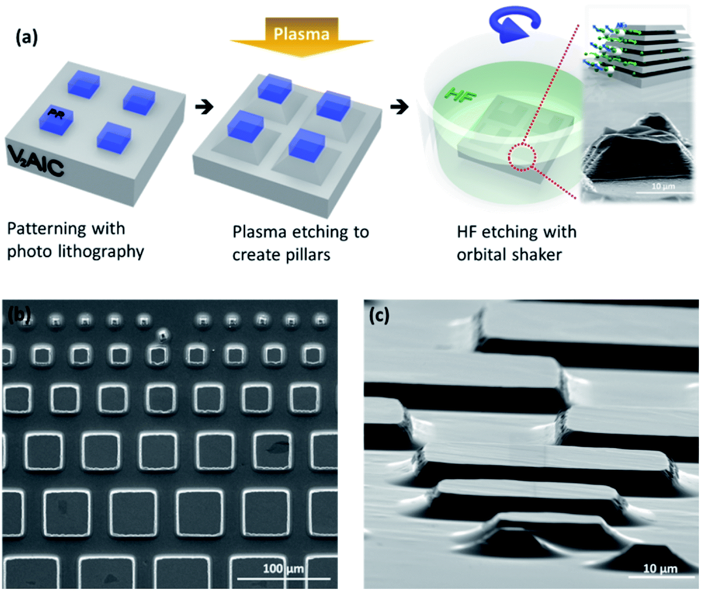 | ||
| Fig. 1 (a) Schematic view of the V2AlC pillars construction and HF etching process; SEM images of the V2AlC pillars, in (b) a top view and (c) a 82° tilted view. | ||
Etching of defective pillars
Quite early on in this work it was obvious that not all pillars etched equally or uniformly. Fig. 2 highlights various pillars where etching was clearly accelerated by the presence of defects and/or stresses. Here the same sample was etched for 6, 15, 24, 33 and 40 h in 49% HF, and observed using a scanning electron microscope (SEM) after washing (Fig. 2a and b), with a backscattered electron (BSE) detector in Fig. 2c, and by EDS mapping of the Al element in Fig. 2d. Due to the fact that the single crystals remain in the growth flux during the final cooling stage, large mechanical stresses can develop. As a consequence, stress does not only favor chemical etching, but also favors a preferential etching of some particular layers: the growing of any small etching fluctuation in the various A layers is favored by the high stress and results in a macroscopic opening of the pillar well before conversion of all other layers. In other words, highly stressed pillars tend to open, and they do so preferentially at particular regions. This is shown in Fig. 2b, and also in Fig. S1.† Those pillars detached from the bulk crystal surface well before the full conversion to MXene was completed.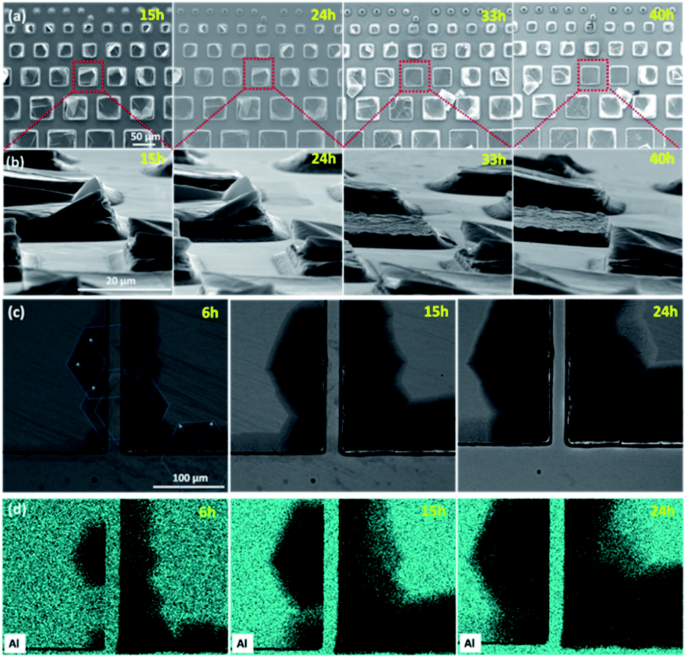 | ||
| Fig. 2 (a) SEM images of V2AlC pillars with various sizes and (b) corresponding 82° tilted views of red dotted square in images in (a) as a function of HF etching time. (c) SEM images and (d) EDS mapping of Al atom lines, of a 500 μm sized pillar as a function of HF etching time. Arrows in (c) indicate preferred etching directions, tracing in some cases hexagon-like structures. | ||
Fig. 2c shows how localized defects located at, or close to, the edges can also speed up chemical exfoliation. Starting from the initial defect location, large ripples forming a star-shaped pattern centered on the initial defect, with directions separated by angles of π/3, progressively extend with time over the surface of a 500 μm sized pillar. Each main ripple gives in turn birth to a set of smaller, lateral ripples. The darker color exhibited by the hexagonal patterns when observed in the backscattered electron (BSE) mode in the SEM images clearly indicates Al removal, as fully confirmed by the EDS maps shown in Fig. 2d, and thus conversion into MXene. The growth direction of V2AlC is highly anisotropic, resulting in a very low crystal aspect ratio30 and most of the V2AlC single crystals have the lateral size of around 1 cm2 and thickness below a few 100 μm. The top surface of the pillars is thus always parallel to an ab plane, and perpendicular to the c axis. In this regard, the hexagonal patterns are clearly crystallographic since all patterns have the same orientations, regardless of their initial positions. These micrographs prove that in the presence of a local stress field, chemical conversion is anisotropic in the ab plane. A tempting, and plausible explanation, is that in the regions of high strain, the F ions penetrate more easily along directions that are less dense in Al atoms.
Fig. 2 shows that the lateral etching distance could exceed 100 μm after 24 h of etching. Similar patterns were observed for other pillars (Fig. S2†), and permitted to fully etch 40, 50 and 90 μm sized pillars (Fig. S3–S5†). Finding such patterns is not only interesting per se, but is also quite useful in order to determine crystal orientations. As seen in Fig. 2c, for this particular crystal, one pillar side is almost directed parallel to the side of the etched hexagonal patterns (misorientation is less than a very few degrees). This implies that the “horizontal” square sides in Fig. 2c and the “vertical” ones respectively correspond to the two extremal possible in-plane crystal orientations. As described below, observing the etching kinetics of each of those sides on defect-free pillars belonging to the same crystal can thus also give us information about the intrinsic, in-plane etching anisotropy.
Etching of defect-free pillars
We now focus on defect-free pillars and/or those with low internal stresses. As shown in Fig. S1b and S6,† the hallmark of these pillars is that they maintain their shape even after etching in 49% HF for 96 h. We expect the results obtained from such pillars to be more representative of the intrinsic etching rates. In this sense intrinsic means not mediated by defects and/or residual stresses. Fig. 3 presents, at different etching times, OM views of a 110 × 110 μm2 sized pillar (Fig. 3a), BSE mode SEM images (Fig. 3b), Al EDS maps (Fig. 3c) and EDS line profiles measured for the V, Al and F elements, respectively (Fig. 3d, e and f). The profile locations were selected in order to avoid any possible shadowing effects. The OM views clearly show a contrast change close to the pillar edges, which progressively extends towards the pillar's center (Fig. 3a). This contrast change is directly correlated to the removal of Al, as attested by the BSE SEM images (Fig. 3b) and Al EDS maps (Fig. 3c). These results show, once again, that the MAX to MXene conversion starts from the edges and moves inwards.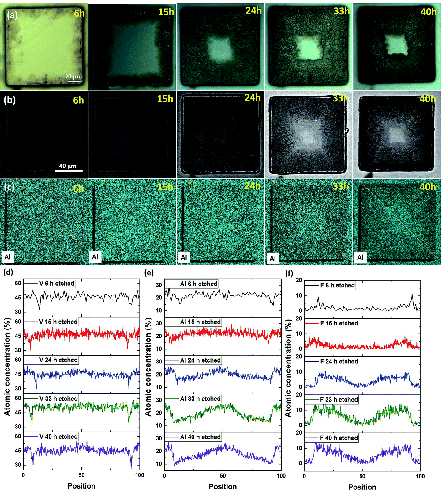 | ||
| Fig. 3 (a) Optical microscope images: (b) BSE mode SEM images, (c) Al EDS maps of a 110 μm sized defect-free V2AlC pillar and EDS line profiles measured for (d) V, (e) Al, (f) F elements as a function of etching time. | ||
Interestingly a progressive depletion of V along the pillar edges is also observed (Fig. 3d). The substantial increase of F atomic concentration, also extending in time towards the pillar center, is consistent with etching starting at the edges. Unfortunately, the presence of adsorbed oxygen (or native oxide subsequently formed in air) on all surfaces, combined with the low O weight and thus low Kα1 energy, made it impossible to quantify the presence of O inside the chemically converted regions.
In a 30 × 30 μm2 sized pillar, the Al signal almost totally disappeared after 15 h of etching time, whereas the F atom concentration reached a homogeneous level throughout the pillar surface (Fig. S7†). This result implies that the etched regions are slowly functionalized by F groups, and, more importantly, that conversion prevalently occurs by edge exposition, and not normal to the basal planes.
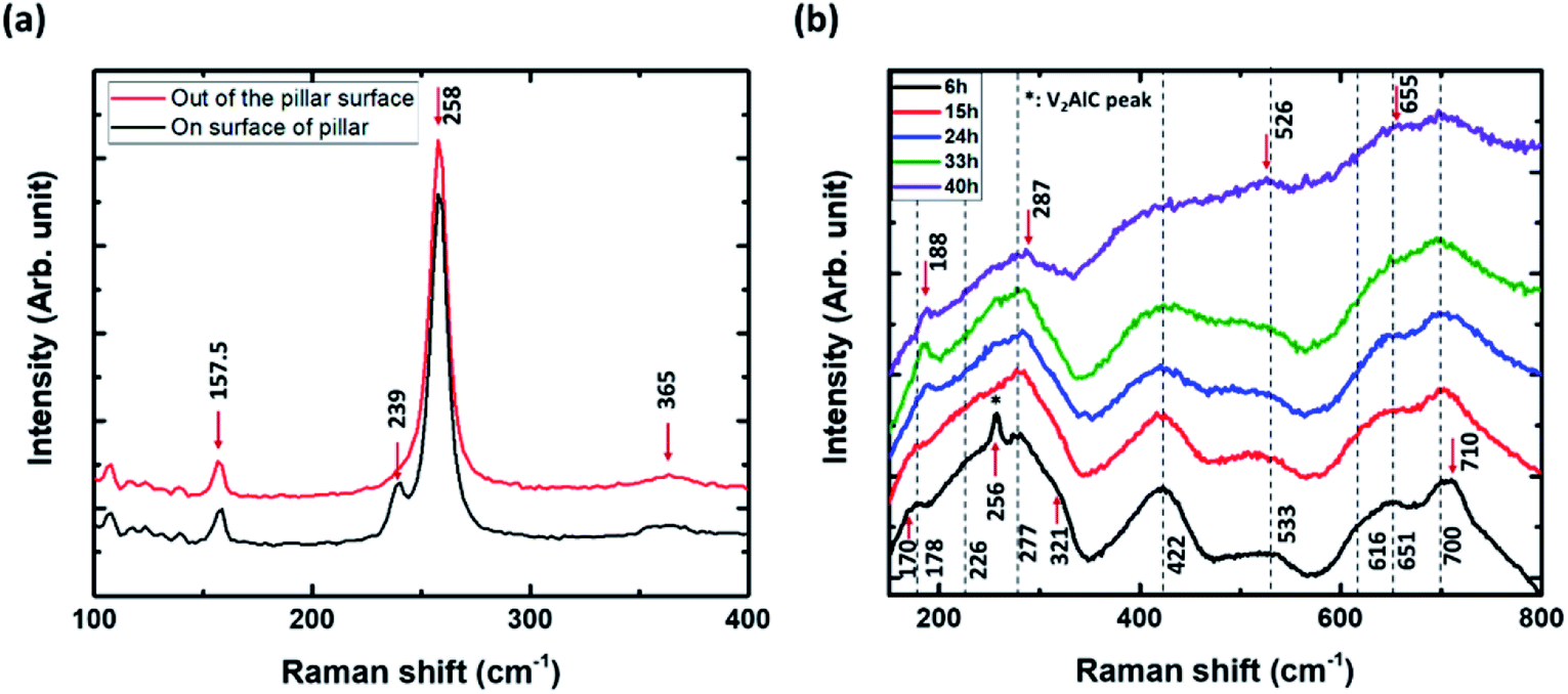
It is also worth noting that supposedly defect-free pillars present no substantial inhomogeneities in their etching fronts, and that there is no appreciable dependence of the etching on the in-plane orientation (see Fig. 3a), since, as shown by Fig. 3, perpendicular edges do not exhibit appreciable differences, whereas they were almost aligned along the two extreme possible orientations in the ab plane, as discussed in the previous section. In order to assess if, (i) etching anisotropy is total (i.e. no transformation is occurring through the ab planes), (ii) the etching front monitored in Fig. 3 can safely be used to quantify the etching kinetics, and (iii) the converted parts are MXenes, we combined the aforementioned observations with micro-Raman spectroscopy. The details can be found in the Experimental section. All the Raman modes observed in this study are reported in Table 1. Fig. 4a compares the Raman spectra at the top of an un-etched pillar (black) and in the channels, or trenches, between the pillars (red). All the Raman modes of V2AlC30,32,34 are detected on top of the un-etched V2AlC pillar (E2g modes at 157.5 and 258 cm−1, E1g at 239 cm−1 and A1g at 365 cm−1). At the bottom, where the surface was exposed to plasma-assisted RIE etching, the Raman peak located at 239 cm−1 has almost disappeared, probably due to some minor surface modification of V2AlC, that results in a decrease of the E1g mode intensity and also produces a quite small shift in the E2g Raman modes.
| V2AlC mode symmetry (SG P63/mmc) | E2g | E1g | E2g | A1g | |||||||
| V2AlC exp [this work] | 157.5 | 239 | 258 | ∼365 | |||||||
| V2AlC exp33 | 158 | 239 | 258 | 360 | |||||||
| V2AlC exp30 | 158 | 239 | 259 | 362 | |||||||
| V2AlC exp32 | 157.4 | 239.1 | 257.3 | 364.2 | |||||||
| V2AlC calc32 | 157 | 254 | 255 | 345 | |||||||
V2C mode symmetry (SG P![[3 with combining macron]](https://www.rsc.org/images/entities/char_0033_0304.gif) m1) m1) |
Eg | A1g | |||||||||
| V2C calc33 | 224 | 359 | |||||||||
| V2CF2 mode symmetry (SG Pm1) |
Eg | A1g | Eg | A1g | |||||||
| V2CF2 calc33 | 198 | 290 | 282 | 526 | |||||||
| V2C(OH)2 mode symmetry (SG Pm1) |
Eg | A1g | Eg | Eg | A1g | A1g | |||||
| V2C(OH)2 calc33 | 214 | 301 | 297 | 443 | 530 | 3613 | |||||
| V2CF(OH) mode symmetry (SG P3m1) | E | E | A1 | E | E | A1 | A1 | A1 | E | A1 | |
| V2CF(OH) calc33 | 196 | 240 | 293 | 297 | 434 | 459 | 534 | 632 | 759 | 3617 | |
| 6 h etched V2AlC [this work] | ∼170 | ∼226 | ∼256 | 277 | ∼321 | ∼422 | ∼533 | ∼616 | ∼700 | ||
| 178 | ∼651 | ∼710 | |||||||||
| 40 h etched V2AlC [this work] | 188 | ∼226 | — | 287 | — | ∼422 | ∼526 | ∼655 | ∼700 | ||
| 72 h etched V2AlC33 | ∼170 | ∼230 | ∼270 | ∼430 | ∼540 | ∼650 | ∼3600 |
 | ||
| Fig. 4 Representative Raman spectra measured (a) at the top surface of an un-etched V2AlC pillar and in the trench area exposed to a chlorine RIE etching process, (b) on a V2CTz area etched by HF for 6 h, 15 h, 24 h, 33 h and 40 h. | ||
Fig. 4b shows V2CTz Raman peaks of converted areas of the pillars after HF etching for 6 h, 15 h, 24 h, 33 h and 40 h. The spectra are composed of quite broad peaks. With increasing etching time from 6 h to 40 h, some of them are shifted (178 to 188 cm−1, 277 to 287 cm−1, 533 to 526 cm−1, 651 to 655 cm−1), others remain un-changed (226, 422, 700 cm−1) or disappear or merge (256, 321, 616, 710 cm−1). After 40 h of etching, the spectra are quite similar to those previously reported for V2CTz33 and most of the peaks match well with the calculated Raman modes of terminated V2CTz (T = F, OH) MXenes (see Table 1). Here we note that the V2C surface can accommodate different types of functional groups, which are presumably randomly distributed and can influence the existence and position of the various peaks.33,35 Especially, the peaks at 188, 655 and 700 cm−1 can only be explained by the formation of V2CF(OH), with F on one side and OH on the other side of the sheets.33 As seen in Table 1 and calculated in ref. 33, they do not exist in the calculated spectra of V2C, V2C(OH)2 or V2CF2. Moreover, the Raman peak located at 256 cm−1 could be assigned to a partially un-etched V2AlC area. This confirms the conversion into MXene and allows us to monitor the Raman signature at a given location as a function of etching time. Fig. 5 shows the time evolution of the Raman spectra: (a) at center of the pillar, around 50 μm away from an edge, (b) in a trench between pillars, (c) on pillar tops but around 30 μm from the edge, and (d) on the top of a pillar but quite close to an edge.
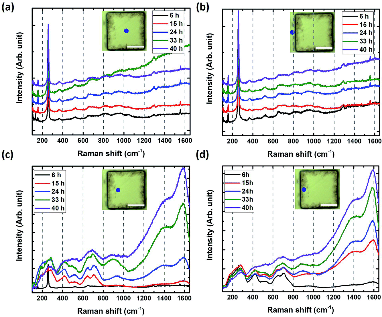 | ||
| Fig. 5 HF etching time dependence of a V2AlC pillar. Raman spectra measured (a) at the center of the pillar surface, (b) in the trench between pillars, (c) on the top of the pillar around 30 μm from the edge, (d) on top of the pillar quite close to the edge. The blue dots in inset shows measured positions (scale bar = 50 μm). | ||
The spectra in the trench area and the pillar center were identical to those of the original V2AlC even after 40 h of etching (Fig. 5a and b). This is an important finding, since it demonstrates that the HF does not penetrate through the ab (basal) planes. Said otherwise, edges need to be exposed to the HF acid for etching to occur. Importantly too, the evolution of the spectra measured 30 μm far from the edge clearly shows the conversion into MXene after 6 h to 15 h of etching (Fig. 5c).
Very close to the edge, the transformation occurs during the first 6 h of etching (Fig. 5d). This is an important aspect of V2CTz synthesis, especially if purity is key for targeted applications.
To further investigate this aspect, we compared the Raman intensities of the MXene peak a 287 cm−1 to the C peak at 1600 cm−1. The ratio of both intensities as a function of etching time at various locations is plotted in Fig. 6a. From Fig. 6a, partial carbonization takes place at the edge even just after 6 h whereas it takes 15 h 10 μm from the edge. After 24 h, the carbon signal largely prevails over that of the MXene in all observed converted parts (Fig. 6b). In a linear scale, the ratio seems to saturate to negligible values after 15 h (edge) and 24 h (10 μm far from the edge), but a log–log scale shows a continuous decrease (Fig. 6b). It follows that during etching of V2AlC, it is important to keep tabs of the carbonization. This carbonization results from the dissolution of some V atoms into the etching solution. Additional and similar results are also provided in the ESI (Fig. S8 and S9†).
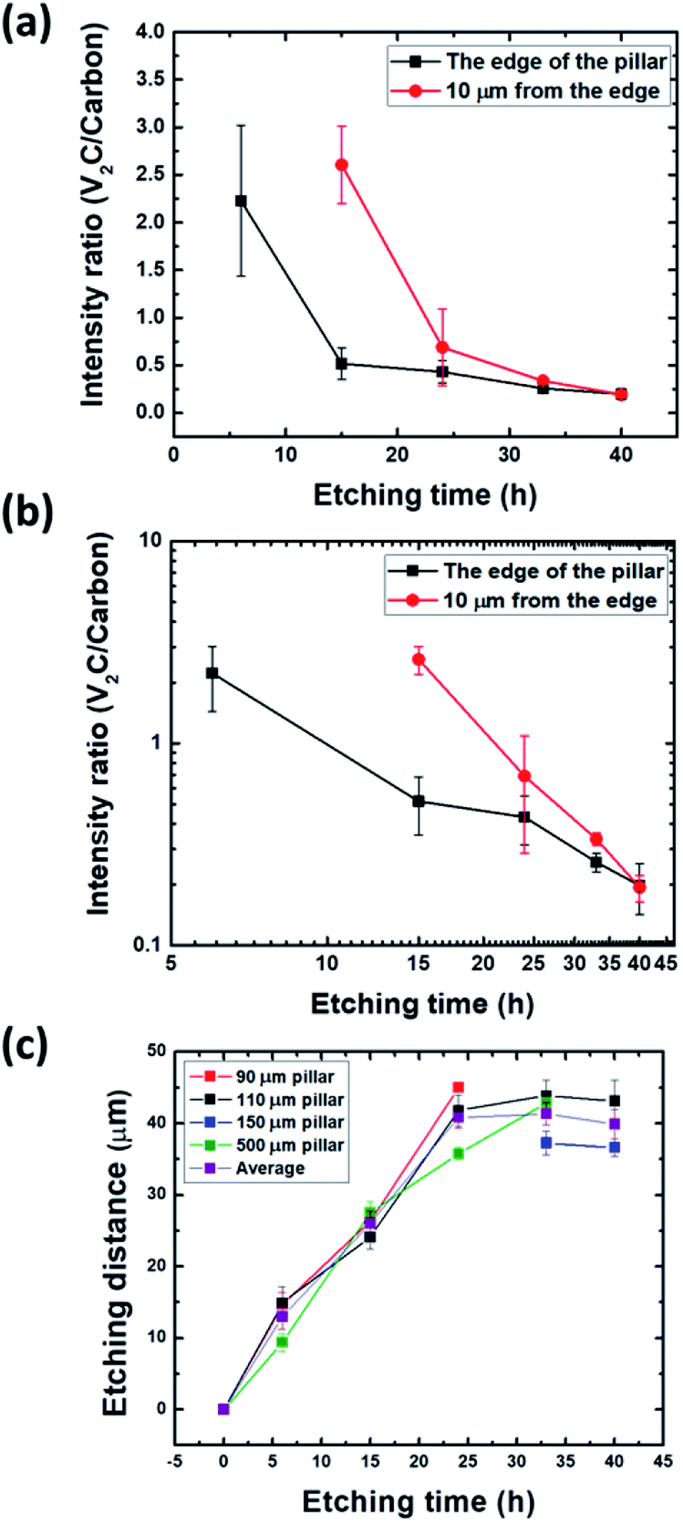 | ||
| Fig. 6 (a) Intensity ratio of V2CTz (∼287 cm−1) to C (∼1600 cm−1) Raman peaks after HF etching of V2AlC pillars as a function of HF etching time. Each square represents the average of 5 points on a given pillar, error bars represent the standard deviation of many pillars; (b) same as (a) but on a log scale; (c) extent of etching penetration as a function of HF etching time for 4 different pillar sizes. Each square represents an average of 20 points, error bars represent the standard deviation. The curve with purple squares is the average obtained from all the pillars. | ||
All Raman measurements indicate that the V2AlC regions which have been converted or transformed by HF etching, as observed in Fig. 3, exhibit the characteristic MXene Raman signature. Therefore, we can safely use those images to monitor the evolution of the boundary between the converted and non-converted areas. These results suggest that after etching V2AlC powders in HF, it is important to measure their Raman spectra to try and quantify if any fraction of the material is carbonized.
Fig. 6c shows the progression of the etching front versus time. After a roughly linear increase, a saturation is clearly observed. More specifically up to a penetration depth of about ≈25 μm, it is reasonable to assume that the reaction rate is controlled by the interface. This is an important conclusion since it implies that diffusional limitations should not play much of a role for powders with particle sizes < 10 μm. This conclusion, however, is at odds with typical etching protocols where the etching time for – 400 mesh powders (< 38 μm) at room temperature is about three days. This point, however, can be related to the saturation observed after one day (Fig. 6c), even if what happens after the linear regime is unclear, whether the process becomes controlled by the diffusion rate or shuts down totally for unknown reasons. Unfortunately, our data do not allow us to discriminate between the various possible out- and in- diffusion processes, or to identify the diffusing species limiting the chemical conversion process. The maximum etched distance so obtained is around 40 μm after 24 h of etching. This sets a bound to the maximum size that can be etched in a defect-free V2AlC crystal, to around 100 μm. In the linear part at the early stage, the etching rate is around 2.2 ± 0.3 μm h−1 at 25 °C.
From the results described above, we decided to assess the possibility to etch small, as-grown, V2AlC single crystals. After etching a solidified growth flux in hydrochloric acid (HCl) and proper filtering, we selected different crystals of various sizes by sieve shaking using 100, 200, 300 and 500 μm grid sizes, and etched them using 49% HF for 7 days at room temperature. After HF etching, we used tetrabutylammonium hydroxide (TBAOH) for the delamination process and vacuum filtration for measuring their X-ray diffraction (XRD) patterns and comparing them. The results, shown in Fig. S10,† all indicate a substantial, but nevertheless incomplete, conversion into MXenes, even after etching times of up to 7 days. Since all crystal sizes are above twice the maximum etching distance determined from Fig. 6c, it seems to confirm a saturation of the chemical conversion as that displayed in the same figure (see the legend of Fig. S10† for a more thorough discussion).
Conclusions
By fabricating single-crystalline pillars, designed with various dimensions and by studying their conversion into MXenes – by etching them in 49% HF – as a function of position and time, we draw the following important conclusions: (i) HF penetration and etching essentially take place through facets oriented perpendicular to the basal planes, the latter being mostly immune to HF penetration. (ii) The etching rate is initially linear at around 2.2 ± 0.3 μm h−1, but slows down considerably at distances > 40 μm; (iii) The HF process gradually leads to a partial carbonization of the converted layers, a major concern if one desires to maximize the convertible crystal size.Last, but not least, the successful conversion of well-defined, single crystalline pillars paves the way to produce and report on less defective and better-controlled MXene layers on various substrates, in order to study their intrinsic electronic or other properties.
Experimental details
V2AlC single crystal growth and pillar fabrication
Single crystals of V2AlC were grown in a high temperature solution as described elsewhere.30 We selected centimeter-sized crystals that were a few hundreds of micrometers in thickness for fabricating the pillars. The crystals were first cut into 5 × 5 mm2 squares using a diamond wire saw. In order to ensure good uniformity of the crystal surfaces, we cleaved them one or two times using a strong adhesive tape, sticking the crystal onto one part of the tape, folding the second part on top of the crystal and peeling off the tape abruptly.30We then covered the crystal surface with a 10 to 12 μm-thick layer of SPR220 photoresist using a spin coater. The resist was baked for 90 s at 115 °C on a hot plate after which the system was allowed to relax for one hour inside a hood. For creating the array of square pillars with different sizes, we prepared a chromium oxide mask with the requisite array pattern. The size of the design corresponded to the V2AlC single crystal dimensions (5 × 5 mm2). The design was composed of horizontal lines with squares whose sides ranged in size from 4 μm to 500 μm. The distance between the rows of squares was 12 μm. The lithography step was carried out in a deep UV Aligner by adjusting properly the mask and the crystal on the apparatus holder. The resist was exposed to a 365 nm wavelength UV light with a power of 0.22 mW cm−2 and a dose of 900 mJ cm−2 for a total duration of ≈ 70 minutes (time = dose/power). Once the lithography step was completed, a ¾ h relaxation inside the hood was needed to allow the water (necessary to complete the photo-reaction) to diffuse back into the photoresist film. For pattern development, the V2AlC crystal was dipped into a MF 26A microposit developer for 6–7 minutes. A final step of hard bake at 100 °C for 4 minutes was necessary to improve the photoresist adhesion during the dry etching process.
Pillars were formed by etching the crystals using an inductively coupled plasma (ICP) high power apparatus which is available in the Upstream Technological Platform (PTA) in French Alternative Energies and Atomic Energy Commission (CEA). Before loading the sample in the apparatus chamber, a Si wafer with a 1 μm thick top SiO2 layer was used for sticking the crystal with a residue-free glue on a hot plate at 65 °C. Then, the wafer was loaded into the ICP chamber and a combination of Cl2 with BCl3 gases was used to etch the crystal for 4–5 minutes using an RF power of 150 W. We optimized the etching conditions depending on the RF power and gas flow. Other gases such as argon or oxygen were tested to etch the V2AlC crystal, but none of them were effective.
After etching, the V2AlC crystal was removed from the wafer by heating it on a hot plate to 65 °C and then it was washed with deionized water. In order to completely remove the remaining photoresist on top of the crystal after etching, we immersed it in a N-methyl-2-pyrrolidone (NMP) bath for 1 h at 80 °C. The minimum pillar size for the RIE etching process was < 7 × 7 μm2. Final pillar height was around 5 μm, with areas ranging from 7 × 7 μm2 to 500 × 500 μm2.
Hydrofluoric etching process: The crystal with the pillar structures was dipped into 20 ml of 49% HF at 25 °C and rotated with an orbital shaker in order to favor homogeneous etching. After reaching the desired etching time, the V2AlC pillars were washed with deionized water several times until the pH value reached 6.
Raman spectroscopy
Raman spectra were recorded using a Jobin Yvon/Horiba Labram spectrometer equipped with a liquid nitrogen cooled CCD detector. The experiments were conducted in the micro-Raman mode in a backscattering geometry at room temperature using the 488 nm excitation line of an Ar+ laser. The laser was focused on the sample surface using a 100× objective with a power close to 2.5 mW. The spot size on the sample was smaller than 1 μm. Raman spectra were calibrated using a silicon spectrum collected at room temperature.Scanning electron microscope and energy-dispersive X-ray spectroscopy
A FEI QUANTA 250 environmental SEM FEG was used to observe the morphology of the V2AlC pillars and a Bruker AXS-30 mm2 SDD detector with a 15 kV acceleration voltage for EDS measurements.Conflicts of interest
There are no conflicts to declare.Acknowledgements
This work was financially supported by “Agence Nationale de la Recherche” (project ANR-18-CE09-0041) and a chair-of-excellence program of the Nanosciences Foundation (Université Grenoble-Alpes Foundation). This work was partly supported by the French RENATECH network.Notes and references
- M. Naguib, M. Kurtoglu, V. Presser, J. Lu, J. Niu, M. Heon, L. Hultman, Y. Gogotsi and M. W. Barsoum, Adv. Mater., 2011, 23, 4248–4253 CrossRef CAS PubMed.
- A. D. Dillon, M. J. Ghidiu, A. L. Krick, J. Griggs, S. J. May, Y. Gogotsi, M. W. Barsoum and A. T. Fafarman, Adv. Funct. Mater., 2016, 26, 4162–4168 CrossRef CAS.
- G. Ying, S. Kota, A. D. Dillon, A. T. Fafarman and M. W. Barsoum, FlatChem, 2018, 8, 25–30 CrossRef CAS.
- L. Ding, Y. Wei, L. Li, T. Zhang, H. Wang, J. Xue, L.-X. Ding, S. Wang, J. Caro and Y. Gogotsi, Nat. Commun., 2018, 9, 155 CrossRef PubMed.
- L. Ding, Y. Wei, Y. Wang, H. Chen, J. Caro and H. Wang, Angew. Chem., Int. Ed., 2017, 56, 1825–1829 CrossRef CAS PubMed.
- A. VahidMohammadi, A. Hadjikhani, S. Shahbazmohamadi and M. Beidaghi, ACS Nano, 2017, 11, 11135–11144 CrossRef CAS PubMed.
- M. Ghidiu, M. R. Lukatskaya, M.-Q. Zhao, Y. Gogotsi and M. W. Barsoum, Nature, 2014, 516, 78–81 CrossRef CAS PubMed.
- X. Liang, A. Garsuch and L. F. Nazar, Angew. Chem., Int. Ed., 2015, 54, 3907–3911 CrossRef CAS PubMed.
- M. R. Lukatskaya, O. Mashtalir, C. E. Ren, Y. Dall'Agnese, P. Rozier, P. L. Taberna, M. Naguib, P. Simon, M. W. Barsoum and Y. Gogotsi, Science, 2013, 341, 1502 CrossRef CAS PubMed.
- F. Shahzad, M. Alhabeb, C. B. Hatter, B. Anasori, S. Man Hong, C. M. Koo and Y. Gogotsi, Science, 2016, 353, 1137–1140 CrossRef CAS PubMed.
- H. Zhang, Z. Wang, Q. Zhang, F. Wang and Y. Liu, Biosens. Bioelectron., 2019, 124–125, 184–190 CrossRef CAS PubMed.
- Y. Lei, W. Zhao, Y. Zhang, Q. Jiang, J.-H. He, A. J. Baeumner, O. S. Wolfbeis, Z. L. Wang, K. N. Salama and H. N. Alshareef, Small, 2019, 15, 1901190 CrossRef PubMed.
- J. Liu, X. Jiang, R. Zhang, Y. Zhang, L. Wu, W. Lu, J. Li, Y. Li and H. Zhang, Adv. Funct. Mater., 2019, 29, 1807326 CrossRef.
- D. Huang, Y. Xie, D. Lu, Z. Wang, J. Wang, H. Yu and H. Zhang, Adv. Mater., 2019, 31, 1901117 CrossRef PubMed.
- M. Sokol, V. Natu, S. Kota and M. W. Barsoum, Trends Chem., 2019, 1, 210–223 CrossRef.
- M. W. Barsoum, Prog. Solid State Chem., 2000, 28, 201–281 CrossRef CAS.
- Z. M. Sun, Int. Mater. Rev., 2011, 56, 143–166 CrossRef CAS.
- M. Naguib, V. N. Mochalin, M. W. Barsoum and Y. Gogotsi, Adv. Mater., 2014, 26, 992–1005 CrossRef CAS PubMed.
- M. Naguib, O. Mashtalir, J. Carle, V. Presser, J. Lu, L. Hultman, Y. Gogotsi and M. W. Barsoum, ACS Nano, 2012, 6, 1322–1331 CrossRef CAS PubMed.
- B. Soundiraraju and B. K. George, ACS Nano, 2017, 11, 8892–8900 CrossRef CAS PubMed.
- T. Li, L. Yao, Q. Liu, J. Gu, R. Luo, J. Li, X. Yan, W. Wang, P. Liu, B. Chen, W. Zhang, W. Abbas, R. Naz and D. Zhang, Angew. Chem., Int. Ed., 2018, 57, 6115–6119 CrossRef CAS PubMed.
- M. Li, J. Lu, K. Luo, Y. Li, K. Chang, K. Chen, J. Zhou, J. Rosen, L. Hultman, P. Eklund, P. O. Å. Persson, S. Du, Z. Chai, Z. Huang and Q. Huang, J. Am. Chem. Soc., 2019, 141, 4730–4737 CrossRef CAS PubMed.
- W. Sun, S. A. Shah, Y. Chen, Z. Tan, H. Gao, T. Habib, M. Radovic and M. J. Green, J. Mater. Chem. A, 2017, 5, 21663–21668 RSC.
- M. Naguib, J. Halim, J. Lu, K. M. Cook, L. Hultman, Y. Gogotsi and M. W. Barsoum, J. Am. Chem. Soc., 2013, 135, 15966–15969 CrossRef CAS PubMed.
- L. Verger, V. Natu, M. Carey and M. W. Barsoum, Trends Chem., 2019, 1, 656–669 CrossRef.
- M. Khazaei, A. Ranjbar, K. Esfarjani, D. Bogdanovski, R. Dronskowski and S. Yunoki, Phys. Chem. Chem. Phys., 2018, 20, 8579–8592 RSC.
- F. Liu, J. Zhou, S. Wang, B. Wang, C. Shen, L. Wang, Q. Hu, Q. Huang and A. Zhou, J. Electrochem. Soc., 2017, 164, A709–A713 CrossRef CAS.
- R. Thakur, A. VahidMohammadi, J. Moncada, W. R. Adams, M. Chi, B. Tatarchuk, M. Beidaghi and C. A. Carrero, Nanoscale, 2019, 11, 10716–10726 RSC.
- O. Mashtalir, M. Naguib, B. Dyatkin, Y. Gogotsi and M. W. Barsoum, Mater. Chem. Phys., 2013, 139, 147–152 CrossRef CAS.
- L. Shi, T. Ouisse, E. Sarigiannidou, O. Chaix-Pluchery, H. Roussel, D. Chaussende and B. Hackens, Acta Mater., 2015, 83, 304–309 CrossRef CAS.
- T. Ouisse, E. Sarigiannidou, O. Chaix-Pluchery, H. Roussel, B. Doisneau and D. Chaussende, J. Cryst. Growth, 2013, 384, 88–95 CrossRef CAS.
- V. Presser, M. Naguib, L. Chaput, A. Togo, G. Hug and M. W. Barsoum, J. Raman Spectrosc., 2012, 43, 168–172 CrossRef CAS.
- A. Champagne, L. Shi, T. Ouisse, B. Hackens and J.-C. Charlier, Phys. Rev. B Condens. Matter, 2018, 97, 115439 CrossRef CAS.
- J. E. Spanier, S. Gupta, M. Amer and M. W. Barsoum, Phys. Rev. B Condens. Matter, 2005, 71, 012103 CrossRef.
- K. J. Harris, M. Bugnet, M. Naguib, M. W. Barsoum and G. R. Goward, J. Phys. Chem. C, 2015, 119, 13713–13720 CrossRef CAS.
Footnote |
| † Electronic supplementary information (ESI) available. See DOI: 10.1039/d0ra00842g |
| This journal is © The Royal Society of Chemistry 2020 |