DOI:
10.1039/D0RA00123F
(Paper)
RSC Adv., 2020,
10, 9902-9906
ALD Al2O3 gate dielectric on the reduction of interface trap density and the enhanced photo-electric performance of IGO TFT
Received
6th January 2020
, Accepted 21st February 2020
First published on 9th March 2020
Abstract
The amorphous indium gallium oxide thin film transistor was fabricated using a cosputtering method. Two samples with different gate dielectric layers were used as follows: sample A with a SiO2 dielectric layer; and sample B with an Al2O3 dielectric layer. The influence of the gate dielectrics on the electric and photo performance has been investigated. Atomic layer deposition deposited the dense film with low interface trapping density and effectively increased drain current. Therefore, sample B exhibited optimal parameters, with an Ion/Ioff ratio of 7.39 × 10⁷, the subthreshold swing of 0.096 V dec−1, and μFE of 5.36 cm2 V−1 s−1. For ultraviolet (UV) detection, the UV-to-visible rejection ratio of the device was 3 × 10⁵, and the photoresponsivity was 0.38 A W−1 at the VGS of −5 V.
Introduction
Amorphous oxide semiconductors on the basis of thin film transistors have been widely developed in active matrix liquid crystal displays, optoelectronic, and organic light-emitting-diode displays.1–3 Among these amorphous oxide semiconductors, In2O3-based TFTs have attracted considerable attention and were investigated due to their high electron mobility and transparency.4–7 Nevertheless, the In concentration in the active channel layer is relatively high, thereby impeding device performance. Excess In2O3 content produces excess oxygen vacancies in the channel layer. Parthiban et al.8 reported metal cations as carrier suppressors and strong bonders; they control the oxygen defect concentration, according to the bond strength of metal oxide, which can improve and enhance the performance of the device. Hsu et al.9 reported fabrication of an indium titanium zinc oxide TFT and manipulated the O flow ratio during sputtering, which suppresses the excess oxygen vacancies in the active layer. With the increase in O flow ratio, the device performance is improved. Our group previously reported the cosputtering of the indium gallium oxide (IGO) thin film with different deposition powers of the In2O3 target, and the photo and electric properties showed that oxygen vacancies are strongly dependent on the In content.10 According to the relevant study results, the In2O3-based TFTs improved the device performance by different methods. However, these methods degrade the mobility and Ion/Ioff ratio. Hence, we prepared Al2O3 as the gate dielectric to optimize the photo and electric properties. Given the advantages of atomic layer deposition (ALD), such as uniformity and control of deposition, the thin film that is generally used for high k materials or passivation layer for TFTs has low leakage current and interface state densities.11,12 High-k materials, such as Si3N4 (∼7), Al2O3 (∼9), MgO (∼9.8), La2O3 (∼14), and ZrOx (∼15), which increase the drain current due to their high dielectric constant values, improve the transistor device characteristics.13–19 In the present study, the IGO thin film transistor was investigated with different dielectrics. Sample A used SiO2 as a dielectric by wet oxidation. Sample B used Al2O3 as a dielectric prepared by ALD. The IGO thin films with large energy band gap were prepared by radio frequency magnetron sputtering system and can be used for ultraviolet (UV) sensing. The detailed photo and electric performances of the devices are discussed in the following sections.
Device fabrication and characterization
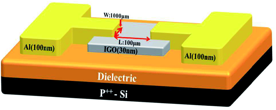
The fabricated samples comprised a Si substrate, a dielectric layer, IGO thin films, and source/drain Al electrodes. Two samples with different dielectric layers were used, as follows: sample A with SiO2 as dielectric layer; and sample B with Al2O3 as dielectric layer. First, the heavily doped p-type Si substrate was ultrasonically cleaned with acetone, methanol, and water for 10 min. Afterward, sample A was grown on a 300 nm SiO2 layer by a wet-oxide tube. Meanwhile, sample B was fabricated on a 70 nm Al2O3 dielectric layer by ALD deposition with precursor trimethylaluminum (TMA) and H2O. The duration times of precursor A (TMA), purge, precursor B (H2O), and purge were 0.1, 4.0, 0.1, and 6.0 s, respectively. The growth rate was 0.094 nm per cycle at 250 °C deposition temperatures.
The IGO channel layer was deposited by cosputtering using Ga2O3 and In2O3 targets with 100 W Ga2O3 power and 60 W In2O3 power, respectively. The growth pressure was fixed on 6 mTorr, with an Ar flow ratio of 3 sccm. The thickness of the channel layer was 30 nm. Afterward, the thin film that was annealed in Ar flow for 60 min at 300 °C. Finally, the Al electrodes were grown at 100 nm using a shadow mask by thermal evaporation. The channel length and width were 100 and 1000 μm, respectively. The electric properties were measured by Agilent B1500 under dark conditions. A 150 W Xe lamp was used to measure the photo properties. The scheme of the IGO TFTs is shown in Fig. 1.
 |
| | Fig. 1 Scheme of IGO TFTs. | |
Results and discussion
Fig. 2 reveals the optical band gap energy of the IGO active layer as calculated by the Tauc plot, which can be extracted by the following equation:where α is the absorbance, Eg is the band gap, and C is the constant. The energy band gap of the IGO thin film is approximately at 4 eV, and the corresponding cut-off wavelength was ∼310 nm. The inset figure shows the transmittance spectra. The films were highly transparent, with over 80% visible region.
 |
| | Fig. 2 Tauc plot of IGO thin film deposited at 300 °C on quartz glass. The inset figure shows the optical transmittance spectra of the IGO thin films. | |
Fig. 3(a) and (b) show the transfer curves and leakage current of samples A and B, respectively, and the extraction averaged value of the two device parameters are listed in Table 1. Two devices were operated in n-type enhancement mode. The threshold voltage was extrapolated from the linear (IDS)1/2–VGS curve. The two devices have very low leakage current value approximately at 10−12 Å which value was negligible. The threshold voltages of sample A and B were 0.8 and 1.3 V, respectively.
 |
| | Fig. 3 Measured transfer characteristics and measured leakage current of (a) sample A and (b) sample B, with different dielectric layer. | |
Table 1 An extraction averaged value of the IGO TFTs with variable dielectric layer
| |
Ion/Ioff ratio (×105) |
SS (V dec−1) |
μFE(cm2 V−1 s−1) |
VTH (V) |
Nt (cm−2 eV−1) (×1011) |
| Sample A |
5.58 ± 2 |
1 ± 0.25 |
1.71 ± 0.34 |
0.6 ± 0.18 |
12.4 ± 1.7 |
| Sample B |
460 ± 260 |
0.1 ± 0.04 |
5.11 ± 0.35 |
1.4 ± 0.25 |
5.89 ± 3.2 |
The field effect mobility (μEF) and subthreshold swing (SS) can be obtained by the following equations:20
| |
 | (2) |
| |
 | (3) |
where
C is the capacitance of the dielectric layer,
W/
L is the channel width and length,
VT is the threshold voltage, and
μ is the saturation mobility. SS is defined as the change in the gate voltage required to increase the drain current by one decade (from 10
−10 Å to 10
−9 Å). The
μEF values of samples A and B were 1.83 and 5.36 cm
2 V
−1 s
−1, and their SS values were 1.2 and 0.096 V dec
−1, respectively. The
Ion/
Ioff ratio that increased by two orders of magnitude were substituted with an Al
2O
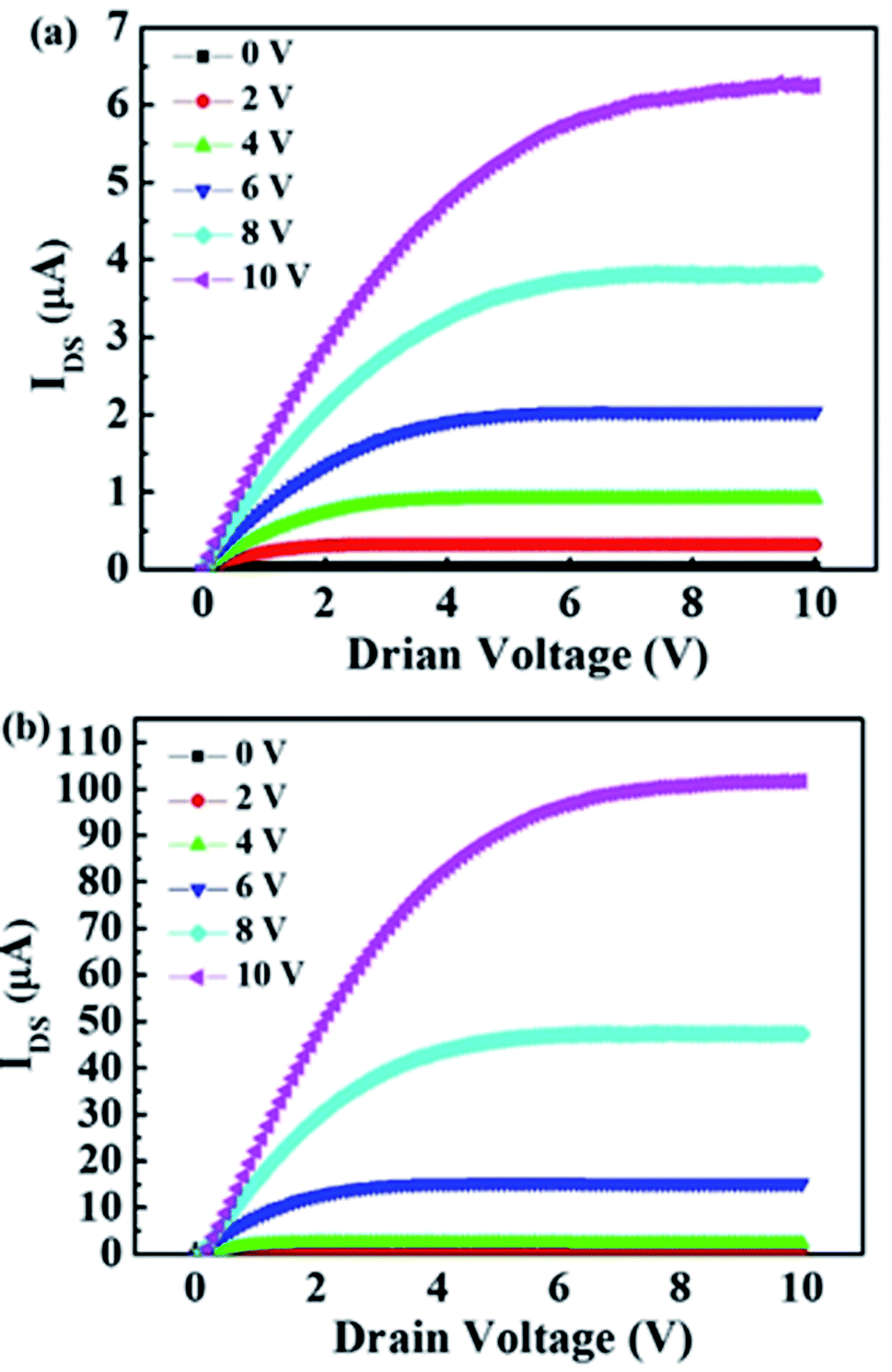
3 dielectric layer. The output characteristics of the two samples with different dielectric layers as a function of the gate overdrive voltage are shown in
Fig. 4. Under the same gate bias, sample B had a higher saturation current compared with sample A, which can attribute the higher dielectric constant. The saturation current of sample A and sample B were 6.25 μA and, 101 μA, respectively. To characterize the interface state density at the channel/dielectric layer, the interface-state trap density (
Nss) can be obtained through the following equation:
21| |
 | (4) |
where
k is the Boltzmann constant, q is the electron charge,
T is the temperature, and is the insulator capacitance per unit area. The interface-state trap densities of samples A and B were 1.37 × 10
12 and 7.50 × 10
11 cm
−2 eV
−1, respectively. The interface trapping density was effectively reduced by the Al
2O
3 layer. The less interface-state trap in sample B could be credited for the dense and uniformity of Al
2O
3 dielectric layer obtained through the ALD deposition process. Moreover, compared with the wet-oxide tube-grown SiO
2 dielectric layer, the Al
2O
3 dielectric layer showed comparative uniformity.
 |
| | Fig. 4 Measured output characteristics of (a) sample A and (b) sample B, with different dielectric layer. | |
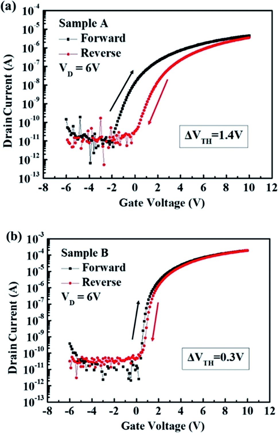
Hence, the hysteresis properties should be improved due to the quality of the dielectric, thereby reducing the Nss. Hysteresis loop measured by sweeping the gate voltage from −6 V to 10 V back and forth. The ΔVT values of samples A and B were 1.4 and 0.3 V, respectively. The large hysteresis of sample A indicated the presence of interface states in the SiO2 layer and that the hysteresis was suppressed in sample B (Fig. 5).
 |
| | Fig. 5 Hysteresis of transfer characteristics of (a) samples A and (b) B, in which sweep range of gate voltage was −6 V from 10 V. | |
As discussed above, the optical energy bandgap of the IGO active layer was approximately at 4 eV, with a corresponding cut-off wavelength of 300 nm. Hence, the IGO active layer has considerable potential as a candidate for UV detection application. Fig. 6 depicts the transfer characteristics of samples A and B, which were measured using a Xe lamp at the wavelength ranging from 480 nm to 250 nm under illumination. The transfer curve from a negative direction moved when the illumination head for short wavelength due to the induced photogenerated carrier, and the light and dark currents increased. The IDS increased possibly due to the following reasons; the photogenerated carrier in the IGO thin film caused by optical absorption; and the fact that ionized Vo can act as a shallow donor state, thereby leading band-to-band excitation under visible illumination, as generally indicated for amorphous oxides.22,23 Consequently, the drain current increased, and the VTH shifted in the negative direction, which can be attributed to carrier generation due to optical absorption and also due to the fact that high dielectric constant can increase the drain current.
 |
| | Fig. 6 Transfer characteristics of (a) sample A and (b) sample B measure in the dark condition and under illumination with various light wavelength (480 nm to 250 nm). | |
The photoresponsivity of the two samples are shown in Fig. 7. The responsivity can be calculated by the following equation:
| |
 | (5) |
where
Iphoto is the photocurrent,
Idark is the dark current, and
Popt indicates the light power. The corresponding responsivities (310 nm) of samples A and B were 0.08 and 0.38 A W
−1, respectively. Sample B exhibited improved response under UV illumination. This result can be attributed to the fact that Al
2O
3 dielectric layer had less trap states and increased gate dielectric constant. UV-to-visible rejection ratio (UV-vis) is the responsivity measured at the peak wavelength of 310 nm divided by the responsivity measured at 450 nm. The UV-vis values of samples A and B were 4 × 10
4 and 3 × 10
5, respectively. Although sample B exhibited good rejection ratio, sample A had excellent rejection ratio, and the two samples were effectively identified through UV radiation. To prepare the IGO thin film transistor with different dielectric layers, we improved the photo and electric performances by replacing the Al
2O
3 dielectric layer. The IGO TFTs can act as a UV phototransistor (
Table 2).
 |
| | Fig. 7 The responsivity of sample A and sample B were measured at various wavelength and VGS of −5 V. | |
Table 2 Photo responsivity and UV-vis of two samples with different dielectric layer
| |
Responsivity (A W−1) @ 310 nm |
UV-vis |
| Sample A |
0.08 |
4 × 10⁴ |
| Sample B |
0.38 |
3 × 10⁵ |
Conclusions
The IGO thin film transistors were investigated with different dielectric layers using SiO2 and Al2O3 (samples A and B, respectively). The influence of the dielectric layer on electrical and photo characteristics has been investigated. The output characteristics shows that a higher dielectric constant can increase the drain current. The Nss was suppressed, which also improved the hysteresis loop, indicated that the interface trapping density effectively reduced via atomic layer deposition. In addition, the device had a UV-vis of 3 × 10⁵, a photoresponsivity of 0.38 A W−1 under a VGS value of −5 V in the 310 nm wavelength region, which is suitable for UV sensing application.
Conflicts of interest
There are no conflicts to declare.
Acknowledgements
This work was supported in part by the Ministry of Science and Technology of Taiwan, ROC, under Grant MOST 107-2221-E-006-185-MY3 and Grant 108-2221-E-006-201-MY3, and in part by the Green Energy Technology Research Center, Department of Electrical Engineering, Kun Shan University, Tainan, Taiwan through The Featured Areas Research Center Program within the framework of the Higher Education Sprout Project by the Ministry of Education (MOE) in Taiwan.
References
- L. Zhang, W. Xiao, W. Wu and B. Liu, Appl. Sci., 2019, 9, 773 CrossRef CAS.
- X. Yu, T. J. Marks and A. Facchetti, Nat. Mater., 2016, 15, 383–396 CrossRef CAS PubMed.
- H. Hosono, J. Kim, Y. Toda, T. Kamiya and S. Watanabe, Proc. Natl. Acad. Sci. U. S. A., 2017, 114, 233–238 CrossRef CAS PubMed.
- J. Smith, L. Zeng, R. Khanal, K. Stallings, A. Facchetti, J. E. Medvedeva, M. J. Bedzyk and T. J. Marks, Adv. Electron. Mater., 2015, 1, 1500146 CrossRef.
- N. Mitoma, S. Aikawa, X. Gao, T. Kizu, M. Shimizu, M.-F. Lin, T. Nabatame and K. Tsukagoshi, Appl. Phys. Lett., 2014, 104, 102103 CrossRef.
- H. Zhang, Y. Meng, L. Song, L. Luo, Y. Qin, N. Han, Z. Yang, L. Liu, J. C. Ho and F. Wang, Nano Res., 2018, 11, 1227–1237 CrossRef CAS.
- Q. Ma, H. M. Zheng, Y. Shao, B. Zhu, W. J. Liu, S. J. Ding and D. W. Zhang, Nanoscale Res. Lett., 2018, 13, 4 CrossRef PubMed.
- S. Parthiban and J.-Y. Kwon, J. Mater. Res., 2014, 29, 1585–1596 CrossRef CAS.
- M. H. Hsu, S. P. Chang, S. J. Chang, W. T. Wu and J. Y. Li, Nanomaterials, 2017, 7, 156 CrossRef PubMed.
- K. Y. Chen, C. C. Yang, Y. K. Su, Z. H. Wang and H. C. Yu, Materials, 2019, 12, 737 CrossRef CAS PubMed.
- P. O. Oviroh, R. Akbarzadeh, D. Pan, R. A. M. Coetzee and T. C. Jen, Sci. Technol. Adv. Mater., 2019, 20, 465–496 CrossRef PubMed.
- B. Wang, W. Huang, L. Chi, M. Al-Hashimi, T. J. Marks and A. Facchetti, Chem. Rev., 2018, 118, 5690–5754 CrossRef CAS PubMed.
- W. J. Scheideler, M. W. McPhail, R. Kumar, J. Smith and V. Subramanian, ACS Appl. Mater. Interfaces, 2018, 10, 37277–37286 CrossRef CAS PubMed.
- C.-H. Lee, N. Vardy and W. Wong, IEEE Electron Device Lett., 2016, 1, DOI:10.1109/led.2016.2557231.
- P. Gogoi, R. Saikia, D. Saikia, R. P. Dutta and S. Changmai, Phys. Status Solidi, 2015, 212, 826–830 CrossRef CAS.
- G. Jiang, A. Liu, G. Liu, C. Zhu, Y. Meng, B. Shin, E. Fortunato, R. Martins and F. Shan, Appl. Phys. Lett., 2016, 109, 183508 CrossRef.
- L. Zhu, G. He, J. Lv, E. Fortunato and R. Martins, RSC Adv., 2018, 8, 16788–16799 RSC.
- W. He, W. Xu, Q. Peng, C. Liu, G. Zhou, S. Wu, M. Zeng, Z. Zhang, J. Gao, X. Gao, X. Lu and J. M. Liu, J. Phys. Chem. C, 2016, 120, 9949–9957 CrossRef CAS.
- N. E. I. Boukortt, B. Hadri and S. Patanè, Int. J. Comput. Sci. Appl., 2016, 139 Search PubMed.
- T. C. Fung, C. S. Chuang, K. Nomura, H. P. D. Shieh, H. Hosono and J. Kanicki, J. Inf. Disp., 2008, 9, 21–29 CrossRef.
- W. Shi, Y. Zheng, J. Yu, A. D. Taylor and H. E. Katz, Appl. Phys. Lett., 2016, 109, 143301 CrossRef.
- S. Jeon, I. Song, S. Lee, B. Ryu, S. E. Ahn, E. Lee, Y. Kim, A. Nathan, J. Robertson and U. I. Chung, Adv. Mater., 2014, 26, 7102–7109 CrossRef CAS PubMed.
- L. S. Feng, G. Y. Yu, X. F. Li, J. H. Zhang, Z. Z. Ye and J. G. Lu, IEEE Trans. Electron Devices, 2017, 64, 206–210 CAS.
|
| This journal is © The Royal Society of Chemistry 2020 |
Click here to see how this site uses Cookies. View our privacy policy here. 
 Open Access Article
 This Open Access Article is licensed under a Creative Commons Attribution-Non Commercial 3.0 Unported Licence
 ab,
Chih-Chiang Yang*b,
Chun-Yuan Huang
ab,
Chih-Chiang Yang*b,
Chun-Yuan Huang