
 Open Access Article
 This Open Access Article is licensed under a Creative Commons Attribution-Non Commercial 3.0 Unported Licence
Recrystallized ice-templated electroless plating for fabricating flexible transparent copper meshes†
Linhai Liab,
Qingrui Fan ab,
Han Xueab,
Shizhong Zhangac,
Shuwang Wua,
Zhiyuan He*a and
Jianjun Wang*ac
ab,
Han Xueab,
Shizhong Zhangac,
Shuwang Wua,
Zhiyuan He*a and
Jianjun Wang*ac
aKey Laboratory of Green Printing, Institute of Chemistry, Chinese Academy of Sciences, Beijing 100190, China. E-mail: wangj220@iccas.ac.cn; hezy@iccas.ac.cn
bSchool of Chemistry and Chemical Engineering, University of Chinese Academy of Sciences, Beijing 100049, China
cSchool of Future Technology, University of Chinese Academy of Sciences, Beijing 100049, China
First published on 9th March 2020
Abstract
Flexible transparent conductors as a replacement for indium tin oxide (ITO) have been urgently pursued due to the inherent drawbacks of ITO films. Here, we report the fabrication of flexible transparent copper meshes with recrystallized ice-crystal templates. Completely different to conventional approaches, this novel method needs neither the fabrication of mesh patterns via micro/nanofabrication technologies nor the deposition of copper through evaporation or sputtering. The linewidth and mesh size of the prepared copper meshes can be regulated, as the ice recrystallization process is controllable. Therefore, the formed copper meshes have tailorable conductivity and transparency, which are critical for optoelectronic devices. Remarkably, the electrical performance of the copper meshes is maintained even after storing for 60 days in ambient conditions or bending for 1000 cycles. This strategy is modular and can also be employed to prepare other metal meshes, such as silver meshes, offering versatile substitutes for ITO in electronic devices.
Introduction
Flexible transparent conductors play an irreplaceable role in electronic devices, including organic light-emitting diodes (OLEDs),1 touch screen displays (TSPs),2 sensors,3 and thin-film solar cells.4 Indium tin oxide (ITO) film is the most commonly used transparent conductor, because it offers relatively low sheet resistance with high transparency.5,6 However, alternatives to ITO film in electronic devices are urgently sought after due to several drawbacks of ITO films. On the one hand, ITO is not suitable for roll-to-roll fabrication processes, nor can it be used in flexible devices because of its brittleness.7 On the other hand, ITO film is expensive, as indium is a rare element and ITO film must be deposited in a low-throughput, inefficient, vapor-phase coating process.8,9In recent years, a rich variety of materials have been investigated for their feasibility to be used as flexible transparent conductors such as metal mesh,10–12 metal nanowire networks,13–15 graphene,16,17 carbon nanotubes,18–20 conducting polymers,21,22 and hybrid materials.23–25 Among them, metal mesh has been shown to be the most promising one, because its electrical conductivity and transparency can be adjusted within a wide range by tailoring the mesh thickness, line spacing, and linewidth.26,27 The most commonly used materials for fabricating metal meshes are copper and silver, due to their high bulk conductivity.28,29 The conductivity of bulk copper is almost the same as that of bulk silver, but copper is 100 times less expensive and 1000 times more abundant than silver; therefore, copper mesh could be an ideal alternative to ITO film.30 As such, intensive research has been carried out to fabricate copper meshes, e.g., copper meshes produced via nanoimprint lithography,31 photolithography,30 ablation by nanosecond laser pulses,6 and with smart masks.27,32 However, most of these methods require lithographic or sputtering processes, which belong to reductive manufacturing and often require the use of relatively expensive instruments. Therefore, it still remains a challenge to fabricate copper meshes with controllable line spacings and linewidths at a low cost.
In this work, copper meshes on polyethylene terephthalate (PET) substrates were constructed via electroless plating with recrystallized ice-crystal templates. The linewidth and mesh size of the copper meshes could be regulated through adjusting the distance between ice grains and the size of ice grains, respectively. Consequently, the transparency and conductivity of the copper meshes on PET films can be tuned, which is critical for optoelectronic devices. The as-prepared flexible transparent copper meshes on PET films exhibit a number of advantages that meet the requirements for replacing commercial ITO film as flexible transparent conductors: (1) the copper meshes on PET films possess low sheet resistance (15.4 Ω sq−1) and high transparency (81.7% at 550 nm), which is comparable to ITO film; (2) this novel approach needs neither the fabrication of mesh patterns via micro/nanofabrication technologies nor the deposition of copper through evaporation or sputtering, which all require expensive instruments; (3) the conductivity of the copper meshes is maintained, even after storing for 60 days under ambient conditions or bending for 1000 cycles.
Experimental section
Materials
CuSO4·5H2O, Na2EDTA, 2,2′-bipyridyl, K4Fe(CN)6, B(N(CH3)2)3 (DMAB), HOCCOOH, NaOH, NaF, NaBr, NaI, H2SO4, toluene, acetone, and 3-aminopropyltrimethoxysilane (APTES) were all purchased from Sigma-Aldrich. Polyethylene terephthalate (PET) film was obtained from Nano Top Ltd.Fabrication of copper meshes on PET films
The original electroless copper plating solution comprises copper sulfate (28 g L−1) as a copper ion source, Na2EDTA (44 g L−1) as a complexing agent, 2,2′-bipyridyl (0.01 g L−1) as a stabilizer, potassium ferrocyanide (0.01 g L−1) as an addition agent, glyoxylic acid (9.2 g L−1) as a reducing agent, and deionized water as the remainder. We diluted the original plating solution to different concentrations, and the pH of the plating solution was adjusted to 12.5–13 with sodium hydroxide. PET substrates were treated with oxygen plasma for 10 min, then immersed into a 5 mM APTES solution for 30 min.33 To remove solvent residue and unreacted silane molecules, the as-prepared PET substrates were consecutively ultrasonically cleaned in toluene, acetone, deionized water, and dried with flowing nitrogen. The fabrication of the copper meshes is shown schematically in Fig. 1a. It involves five steps: (I) a droplet of plating solution was dripped from 1 meter in the air onto a supercooled PET film (−80 °C, modified with APTES) to obtain a uniform thin ice film consisting of a large number of tiny ice crystals. Upon contacting with the PET film, the droplet spread first on the PET film and then froze spontaneously. As the surface temperature of the PET film was far below the homogeneous ice nucleation temperature, ice nucleation occurred spontaneously, forming a large number of tiny ice crystals. (II) The quenched plating solution was annealed at a relatively higher temperatures for 1 hour, and the temperature was kept constant during the whole annealing and reaction process. During the annealing process, the grain size of large ice crystals increased, while small ice crystals disappeared (Fig. S1, ESI†). As a result, the plating solution became trapped and concentrated between ice grains. (III) A droplet of dimethyl ammonium borane (DMAB) solution (5 g L−1) was dripped onto a supercooled cover glass slide (−80 °C) to form a large number of tiny ice crystals. (IV) The as-prepared cover glass slide with an ice film of DMAB was flipped and placed atop the annealed ice film on the PET surface to react for a period of time. During this process, the quenched DMAB solution was annealed; thus, the DMAB solution became concentrated between ice grains, so that the DMAB diffused into the plating solution and became concentrated between the ice grains on the PET surface. The electroless copper plating between the ice crystals could be initiated once the DMAB had diffused into the plating solution, due to the strong reduction of DMAB.33–35 (V) The ice template was removed by washing with ethanol, and the copper meshes were left on the PET substrates. The statistical method followed our reported work.38 The samples with copper meshes were imaged randomly. For every sample, five experimental runs were performed. To plot each figure, the size of the largest 10 meshes was measured using Nano-Measure 1.2, and these 50 data points were chosen to calculate the mean size of the copper meshes.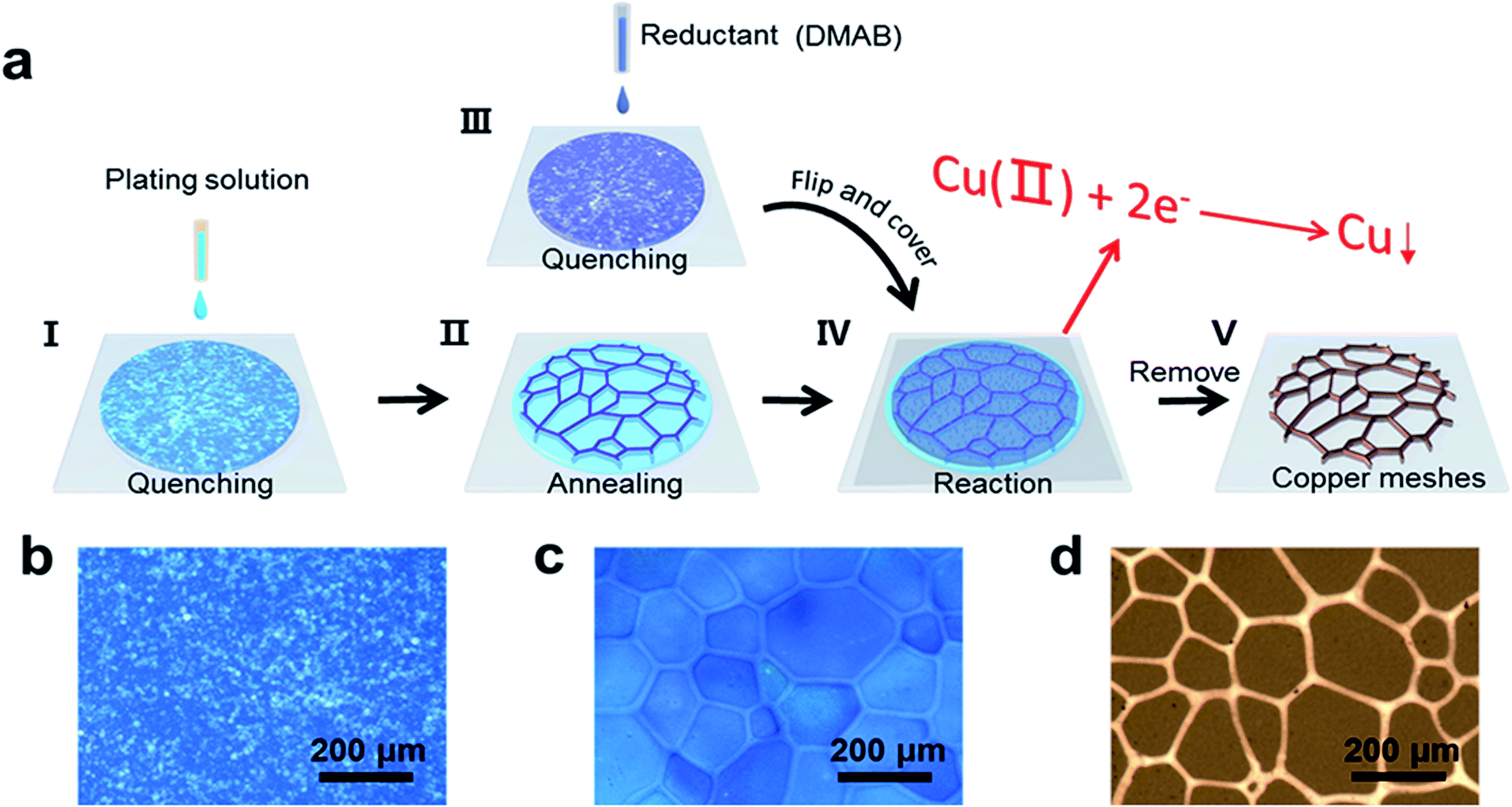 | ||
| Fig. 1 (a) Schematic illustration for the preparation of copper meshes on a PET substrate. (b) Polarized optical microscopy (POM) image of ice crystals formed just after splat-freezing, and a large number of tiny ice crystals can be observed. (c) POM image of recrystallized ice crystals after annealing at −3 °C for 1 hour and much larger ice crystals can be observed. (d) POM image of the copper mesh after removing the ice template. | ||
Characterization
The morphology of the copper meshes was characterized using optical microscopy (Nikon eclipse LV 100ND) and scanning electron microscopy (SEM, JEOL JSM-7500). The thickness of the copper meshes was measured by atomic force microscopy (AFM). The X-ray diffraction (XRD) spectra were obtained on an Empyrean-2 diffractometer. The sheet resistance (RS) was measured using a four-point probe (ST2558B-F03) measurement, and the transparency of the conductive films was characterized using a UV-vis spectrophotometer (UV-9000). The mechanical properties of the copper meshes were measured via a bending test system.Results and discussion
Fig. 1b shows a large number of tiny ice crystals that formed just after splat-freezing. Ice crystals grew obviously larger after annealing at −3 °C for 1 hour, as shown in Fig. 1c. Fig. 1d reveals the interconnected copper mesh after removing the ice template. For comparison, we repeated the fabrication of copper meshes without the annealing step, which resulted in blurred copper meshes (Fig. S2a, ESI†). This phenomenon can be reconciled by considering that the reaction is initiated before the stable ice grains are apparent, as the ice crystals experience an initial growth and then level off after 60 min (Fig. S1, ESI†). It is noted that the annealing of ice crystals is an essential process.Fig. 2a–c show the copper meshes obtained from the electroless copper plating at −3 °C for 25, 120 and 240 min, which become more obvious with the increase of the reaction time. The X-ray diffraction (XRD) pattern presented in Fig. 2d shows the characteristic diffraction peaks of the PET film with copper meshes, displaying the PET diffraction peak as well as the diffraction features of the (111), (200), and (220) planes of the copper crystal. The insets of Fig. 2d and S3 (ESI)† reveal that the copper meshes consist of copper nanoparticles and the diameter of these nanoparticles is about a few tens of nanometers. Atomic force microscopy (AFM) was employed to monitor the evolution of the thickness of the copper meshes with reaction time and reaction temperature, as shown in Fig. 2e and S4 (ESI).† Note that both the rate of thickness growth and the final thickness follow the sequence of −7 °C < −5 °C < −3 °C < −1 °C, i.e., the rate of the reaction and the thickness increase with temperature, which is in agreement with the conventional electroless deposition of copper.36
 | ||
| Fig. 2 The evolution of the thickness of the copper meshes with reaction time and reaction temperature. The concentration of the plating bath is 2.8 g L−1. (a–c) The copper meshes obtained from the electroless copper plating at −3 °C for (a) 25 min, (b) 120 min, and (c) 240 min. (d) X-ray diffraction spectra of PET films with and without copper meshes (the inset shows the SEM image of copper nanoparticles). (e) The change in height of the copper meshes with reaction time at different reaction temperatures. | ||
We further studied the effects of the plating bath concentration and the reaction temperature on the fabricated copper meshes. The linewidth of copper meshes increased with the concentration of the plating solution, as shown in Fig. 3a–c. Fig. 3d reveals that the linewidth of the copper meshes could be tuned from 10.3 ± 0.6 μm to 27.1 ± 0.7 μm as the plating bath concentration was varied from 2.8 g L−1 to 8.4 g L−1 (here and after, the concentration of the plating bath is represented by the concentration of CuSO4·5H2O). In addition, the linewidth of the copper meshes could also be controlled by changing the reaction temperature. When the reaction temperature was increased from −7 °C to −1 °C, the linewidth increased from 8.9 ± 0.4 μm to 10.9 ± 0.3 μm (Fig. 3e). This observation can be explained by considering that the distance between ice grains increases with temperature as well as the concentration of the plating solution (Fig. S5, ESI†). However, when the reaction temperature or the concentration of the plating solution was too low, the copper meshes became un-interconnected (Fig. S2b, ESI†). On the contrary, blurred copper meshes (Fig. S2c, ESI†) were obtained if the reaction temperature or the concentration of the plating solution was too high, as detailed in Fig. 3f.
 | ||
| Fig. 3 Adjusting the linewidth of copper meshes by varying the concentration of the plating bath and temperature. (a–c) The copper meshes obtained from the plating bath with concentrations of (a) 2.8 g L−1, (b) 5.6 g L−1, (c) 8.4 g L−1. (d) The linewidth increases with the concentration of the plating bath (the reaction temperature is −3 °C). (e) The linewidth increases with the reaction temperature (the concentration of the plating bath is 2.8 g L−1). (f) The chart reveals the optimal conditions for manufacturing copper meshes. | ||
Metal meshes have attracted significant attention as flexible transparent conductors, owing to their high conductivities and transmittances. The most commonly-used process of manufacturing metal meshes depends on micro/nanofabrication technologies, including photolithography and nanoimprint lithography.30,31 Recently, Grigoropoulos and co-workers6 produced transparent copper meshes using a new laser direct writing approach incorporating simultaneous patterning, and no structural deformation or damage of the flexible polymer substrate was observed. Furthermore, several novel templates have been researched, which can produce large-scale metal mesh at relatively low cost. Ma and co-workers27 developed an approach to prepare copper mesh electrodes by the breath-figure templating method, in which the optimal and electrical properties of the resulting copper mesh can be tuned by varying the relative humidity. Leu and co-workers32 reported a scalable, facile microsphere-based approach to fabricate metal meshes on rigid quartz and PET substrates. Kempa and co-workers37 developed a new method based on a “cracked” gel film for making metallic networks, and the electrodes are also easy to pattern. However, it still remains a challenge to fabricate metal meshes with controllable line spacing and linewidth at a low cost. In our work, the mesh size of the copper meshes can be adjusted by employing ion-specific effects on ice recrystallization, i.e., varying the type of added ions or ionic concentration in the plating bath.38 Fig. 4a–c show the copper meshes obtained with the addition of NaF, NaBr and NaI (their concentration in the plating solution is 0.2 g L−1) respectively. The corresponding mesh sizes are 41.3 ± 4.6 μm, 213.8 ± 17.9 μm and 281.8 ± 18.6 μm, respectively, following the exact same trend as the ion-specific effects on the size of recrystallized ice grains (Fig. S6, ESI†). Moreover, the mesh size of copper meshes can be further tuned by changing the ionic concentration in the plating solution. As compared in Fig. 4a, d and e, the mesh size of the copper meshes decreases from 208.2 ± 17.1 to 41.3 ± 4.6 μm as the concentration of NaF in the plating solution increases from 0.0 to 0.2 g L−1. However, the effects of changing the concentration of NaBr or NaI in the plating solution is not obvious, as displayed in Fig. 4f. This strategy is modular and can also be employed to prepare other metal meshes, and silver meshes with various sizes were produced based on the same strategy (Fig. S7, ESI†).
 | ||
| Fig. 4 Adjusting the mesh size of copper meshes by changing the type of added ions or ionic concentration in the plating bath. (a–c) The copper meshes obtained from the plating bath with the addition of (a) 0.2 g L−1 NaF, (b) 0.2 g L−1 NaBr, (c) 0.2 g L−1 NaI. (d and e) The copper meshes obtained from the plating bath with the addition of (d) 0.002 g L−1 NaF, (e) 0 g L−1 NaF. (f) The effects of changing the concentration of NaF, NaBr or NaI in the plating solution. The temperature is −3 °C, and the concentration of the plating solution is 2.8 g L−1. | ||
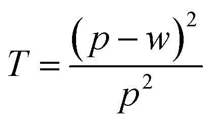
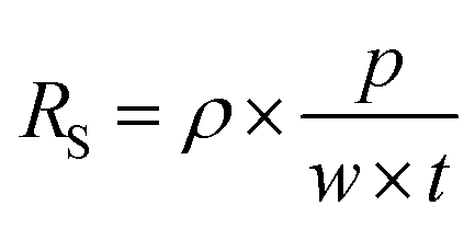
We investigated the effects of the mesh size and linewidth on the sheet resistance and transparency, as shown in Fig. 5a and b, and the transparency spectra of copper meshes with different mean mesh sizes are shown in Fig. S8 (ESI).† The transparency (T) and the sheet resistance (RS) of metal mesh can be calculated using eqn (1) and (2), where w is the linewidth, p is the pore size, t is the thickness of the mesh, and ρ is the resistivity of the metal.39
 | (1) |
 | (2) |
 | ||
| Fig. 5 (a) The change of sheet resistance and transparency at 550 nm wavelength with mesh size (linewidth is 10.3 μm, thickness is 140 nm). (b) The evolution of sheet resistance and transparency at 550 nm wavelength with linewidth (mesh size is 208 μm, thickness is 140 nm). (c) T values as a function of 1/RS sheet with FoM values for various materials: (1) AgCu alloy mesh,44 (2) graphene/Ag grids,45 (3) polymeric acid doped CNTs,46 (4) (RGO)/Au grids,47 (5) modified PEDOT:PSS,48 (6) copper mesh made by nanosecond laser pulse ablation,6 (7) AgNWs,49 (8) PEDOT:PSS/Ag mesh,50 (9) this work. (d) The change of sheet resistance after annealing at 100 °C under vacuum for 30 min. (e) Sheet resistance variation (R/R0) versus the number of cycles of repeated bending to a radius of 3 mm. (f) Oxidation stability of the copper meshes under ambient conditions (the inset shows the digital photo image of a PET film with large area of copper meshes made by impinging the droplet side-by-side). | ||
The data of sheet resistance against the mesh size in Fig. 5a were fitted as follows: RS = 0.147p. The electrical resistivity of the copper meshes was calculated to be ρ = 2.12 × 10⁻⁷ Ω m, which is about ten times higher than that of bulk copper (ρ = 1.75 × 10⁻⁸ Ω m), possibly due to the increased electron transfer barrier between copper nanoparticles.40 An average RS decrease of 30% was observed after annealing at 100 °C under vacuum (Fig. 5d), which can be attributed to the reduced contact resistance between copper nanoparticles.33 The quality of a transparent electrode could also be described in the form of a figure-of-merit (FoM = σdc/σopc), which can be calculated using eqn (3), where σdc and σopc represent direct current conductivity and optical conductivity, respectively.41
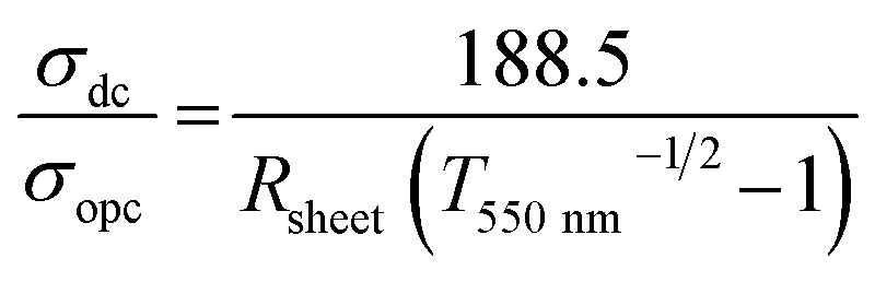 | (3) |
The FoM values of the coper meshes with different mesh sizes and linewidths are shown in Fig. S9 (ESI).† The FoM reaches a maximum of about 115 when the mesh size is 120 μm and the linewidth is 10.3 μm. Fig. 5c presents the comparison of the FoM value of the prepared copper mesh (red star) with other materials. It reveals that the FoM value of the prepared copper mesh is comparable to that of copper mesh made by nanosecond laser pulse ablation (black square),6 which reaches 110 (calculated by eqn (3)) when the sheet resistance is 17.48 Ω sq−1 and the transparency is 83% by optimizing the areal density.
Fig. 5e presents the sheet resistance variation (R/R0) versus the number of cycles for repeated compressive bending to a radius of 3 mm, which signifies the mechanical reliability of the copper meshes. Furthermore, oxidation stability tests under ambient conditions indicated no significant increase in the sheet resistance within 2 months (Fig. 5f). In our case, only the uppermost surface of the copper meshes is oxidized and the copper oxide layer acts as a protecting layer to prevent the oxidization of the internal copper.42 This is why the sheet resistance first increases a little and then remains stable. It is noted that RS increased at a faster rate after 36 days, possibly due to the oxidization of the internal copper as time increases. Moreover, it took about 1000 minutes for the resistance to increase by an order of magnitude at 100 °C (Fig. S10, ESI†). This is remarkable compared to the reported value of a copper network without a protective coating by Jiang et al., which has a thickness of 100–150 nm.30 We further used the tape-test to investigate the adhesive strength between the copper mesh and the PET substrate, and found that RS of the copper mesh increased by 16 times after repeating the tape-tests 10 times (Fig. S11, ESI†). The thermal oxidation stability and adhesion strength may be further increased via many strategies, such as introducing an ionogel layer,30 and incorporation with PEDOT:PSS.43 Fig. S12† shows a digital photo of the copper mesh made from impinging one droplet of plating solution, and a much larger area of copper mesh was obtained by impinging the droplet side-by-side as demonstrated in Fig. 5f.
Conclusions
In summary, we reported a new strategy for the fabrication of flexible transparent copper meshes by combining the electroless plating approach with recrystallized ice-crystal templates. This new approach requires neither the fabrication of mesh patterns via micro/nanofabrication technologies nor the deposition of copper through evaporation or sputtering. The electrical properties of the copper meshes can be easily adjusted by varying the concentration of the plating bath, and the type of added ions or ionic concentration in the plating bath, allowing for various combinations of sheet resistance and transparency to meet the needs of different devices. We demonstrated that the electrical performance of the copper meshes is maintained even after storing in ambient conditions for 60 days or bending for 1000 cycles.Conflicts of interest
There are no conflicts to declare.Acknowledgements
The authors are grateful for the financial support from the Chinese National Nature Science Foundation (51925307, 21733010, and 21875261), National Key R&D Program of China (2018YFA0208502), and Youth Innovation Promotion Association of the Chinese Academy of Sciences (2018044).References
- M. G. Helander, Z. B. Wang, J. Qiu, M. T. Greiner, D. P. Puzzo, Z. W. Liu and Z. W. Liu, Science, 2011, 332, 944–947 CrossRef CAS PubMed.
- D. Lee, D. Paeng, H. K. Park and C. P. Grigoropoulos, ACS Nano, 2014, 8, 9807–9814 CrossRef CAS PubMed.
- P. Wan, X. Wen, C. Sun, B. K. Chandran, H. Zhang, X. Sun and X. Chen, Small, 2015, 11, 5409–5415 CrossRef CAS PubMed.
- W. Gaynor, J.-Y. Lee and P. Peumans, ACS Nano, 2010, 4, 30–34 CrossRef CAS PubMed.
- K. Ellmer, Nat. Photonics, 2012, 6, 809–817 CrossRef CAS.
- D. Paeng, J. H. Yoo, J. Yeo, D. Lee, E. Kim, S. H. Ko and C. P. Grigoropoulos, Adv. Mater., 2015, 27, 2762–2767 CrossRef CAS PubMed.
- D. S. Hecht and R. B. Kaner, MRS Bull., 2011, 36, 749–755 CrossRef CAS.
- M. Cai, Z. Ye, T. Xiao, R. Liu, Y. Chen, R. W. Mayer, R. Biswas, K. M. Ho, R. Shinar and J. Shinar, Adv. Mater., 2012, 24, 4337–4342 CrossRef CAS PubMed.
- D. S. Hecht, L. Hu and G. Irvin, Adv. Mater., 2011, 23, 1482–1513 CrossRef CAS PubMed.
- H. J. Choi, S. Choo, P. H. Jung, J. H. Shin, Y. D. Kim and H. Lee, Nanotechnology, 2015, 26, 055305 CrossRef PubMed.
- A. Khan, S. Lee, T. Jang, Z. Xiong, C. Zhang, J. Tang, L. J. Guo and W. D. Li, Small, 2016, 12, 3021–3030 CrossRef CAS PubMed.
- H. B. Lee, W.-Y. Jin, M. M. Ovhal, N. Kumar and J.-W. Kang, J. Mater. Chem. C, 2019, 7, 1087–1110 RSC.
- J. H. M. Maurer, L. González-García, I. K. Backes, B. Reiser, S. M. Schlossberg and T. Kraus, Adv. Mater. Technol., 2017, 2, 1700034 CrossRef.
- H. Wu, D. Kong, Z. Ruan, P. C. Hsu, S. Wang, Z. Yu, T. J. Carney, L. Hu, S. Fan and Y. Cui, Nat. Nanotechnol., 2013, 8, 421–425 CrossRef CAS PubMed.
- S. Ye, A. R. Rathmell, Z. Chen, I. E. Stewart and B. J. Wiley, Adv. Mater., 2014, 26, 6670–6687 CrossRef CAS PubMed.
- K. S. Kim, Y. Zhao, H. Jang, S. Y. Lee, J. M. Kim, K. S. Kim, J. H. Ahn, P. Kim, J. Y. Choi and B. H. Hong, Nature, 2009, 457, 706–710 CrossRef CAS PubMed.
- J. Ning, L. Hao, M. Jin, X. Qiu, Y. Shen, J. Liang, X. Zhang, B. Wang, X. Li and L. Zhi, Adv. Mater., 2017, 29, 1605028 CrossRef PubMed.
- B. Dan, G. C. Irvin and M. Pasquali, ACS Nano, 2009, 3, 835–843 CrossRef CAS PubMed.
- S. Jiang, P.-X. Hou, M.-L. Chen, B.-W. Wang, D.-M. Sun, D.-M. Tang, Q. Jin, Q.-X. Guo, D.-D. Zhang, J.-H. Du, K.-P. Tai, J. Tan, E. I. Kauppinen, C. Liu and H.-M. Cheng, Sci. Adv., 2018, 4, eaap9264 CrossRef PubMed.
- Z. Wu, Z. Chen, X. Du, J. M. Logan, J. Sippel, M. Nikolou, K. Kamaras, J. R. Reynolds, D. B. Tanner, A. F. Hebard and A. G. Rinzler, Science, 2004, 305, 1273–1276 CrossRef CAS PubMed.
- S. Kee, N. Kim, B. Park, B. S. Kim, S. Hong, J. H. Lee, S. Jeong, A. Kim, S. Y. Jang and K. Lee, Adv. Mater., 2018, 30, 1703437 CrossRef PubMed.
- Y. Xia, K. Sun and J. Ouyang, Adv. Mater., 2012, 24, 2436–2440 CrossRef CAS PubMed.
- B. Deng, P. C. Hsu, G. Chen, B. N. Chandrashekar, L. Liao, Z. Ayitimuda, J. Wu, Y. Guo, L. Lin, Y. Zhou, M. Aisijiang, Q. Xie, Y. Cui, Z. Liu and H. Peng, Nano Lett., 2015, 15, 4206–4213 CrossRef CAS PubMed.
- A. G. Ricciardulli, S. Yang, G.-J. A. H. Wetzelaer, X. Feng and P. W. M. Blom, Adv. Funct. Mater., 2018, 28, 1706010 CrossRef.
- J. H. Yoo, Y. Kim, M. K. Han, S. Choi, K. Y. Song, K. C. Chung, J. M. Kim and J. Kwak, ACS Appl. Mater. Interfaces, 2015, 7, 15928–15934 CrossRef CAS PubMed.
- H. J. Kim, S. H. Lee, J. Lee, E. S. Lee, J. H. Choi, J. H. Jung, J. Y. Jung and D. G. Choi, Small, 2014, 10, 3767–3774 CrossRef CAS PubMed.
- W. Zhou, J. Chen, Y. Li, D. Wang, J. Chen, X. Feng, Z. Huang, R. Liu, X. Lin, H. Zhang, B. Mi and Y. Ma, ACS Appl. Mater. Interfaces, 2016, 8, 11122–11127 CrossRef CAS PubMed.
- X. Chen, S. Nie, W. Guo, F. Fei, W. Su, W. Gu and Z. Cui, Adv. Electron. Mater., 2019, 5, 1800991 CrossRef.
- B. Sciacca, J. van de Groep, A. Polman and E. C. Garnett, Adv. Mater., 2016, 28, 905–909 CrossRef CAS PubMed.
- L. Chang, X. Zhang, Y. Ding, H. Liu, M. Liu and L. Jiang, ACS Appl. Mater. Interfaces, 2018, 10, 29010–29018 CrossRef CAS PubMed.
- M. G. Kang and L. J. Guo, Adv. Mater., 2007, 19, 1391–1396 CrossRef CAS.
- T. Gao, B. Wang, B. Ding, J. K. Lee and P. W. Leu, Nano Lett., 2014, 14, 2105–2110 CrossRef CAS PubMed.
- S. Armini and A. M. Caro, J. Electrochem. Soc., 2010, 157, D74–D80 CrossRef CAS.
- T. Homma, A. Tamaki, H. Nakai and T. Osaka, J. Electroanal. Chem., 2003, 559, 131–136 CrossRef CAS.
- H. Lee, S. M. Dellatore, W. M. Miller and P. B. Messersmith, Science, 2007, 318, 4236–4246 Search PubMed.
- H. Honma and T. Kobayashi, J. Electrochem. Soc., 1994, 141, 730–733 CrossRef CAS.
- B. Han, K. Pei, Y. Huang, X. Zhang, Q. Rong, Q. Lin, Y. Guo, T. Sun, C. Guo, D. Carnahan, M. Giersig, Y. Wang, J. Gao, Z. Ren and K. Kempa, Adv. Mater., 2014, 26, 873–877 CrossRef CAS PubMed.
- S. Wu, C. Zhu, Z. He, H. Xue, Q. Fan, Y. Song, J. S. Francisco, X. C. Zeng and J. Wang, Nat. Commun., 2017, 8, 15154 CrossRef PubMed.
- W. Wu, N. G. Tassi, D. J. Walls, L. Zhang and B. Willner, Appl. Phys. Lett., 2014, 105, 223104 CrossRef.
- D. Zabetakis, P. Loschialpo, D. Smith, M. A. Dinderman and W. J. Dressick, Langmuir, 2009, 25, 1785–1789 CrossRef CAS PubMed.
- M. Dressel and G. Gruner, Electrodynamics of Solids, Cambridge University Press, Cambridge, 2002, vol. 97 Search PubMed.
- K. Li, H. Zhen, L. Niu, X. Fang, Y. Zhang, R. Guo, Y. Yu, F. Yan, H. Li and Z. Zheng, Adv. Mater., 2014, 26, 7271–7278 CrossRef CAS PubMed.
- J. Chen, W. Zhou, J. Chen, Y. Fan, Z. Zhang, Z. Huang, X. Feng, B. Mi, Y. Ma and W. Huang, Nano Res., 2014, 8, 1017–1025 CrossRef.
- M. Mohl, A. Dombovari, R. Vajtai, P. M. Ajayan and K. Kordas, Sci. Rep., 2015, 5, 13710 CrossRef PubMed.
- Y. H. Kahng, M.-K. Kim, J.-H. Lee, Y. J. Kim, N. Kim, D.-W. Park and K. Lee, Sol. Energy Mater. Sol. Cells, 2014, 124, 86–91 CrossRef CAS.
- I. Jeon, C. Delacou, H. Okada, G. E. Morse, T.-H. Han, Y. Sato, A. Anisimov, K. Suenaga, E. I. Kauppinen, S. Maruyama and Y. Matsuo, J. Mater. Chem. A, 2018, 6, 14553–14559 RSC.
- T. Qiu, B. Luo, M. Liang, J. Ning, B. Wang, X. Li and L. Zhi, Carbon, 2015, 81, 232–238 CrossRef CAS.
- N. Kim, H. Kang, J. H. Lee, S. Kee, S. H. Lee and K. Lee, Adv. Mater., 2015, 27, 2317–2323 CrossRef CAS PubMed.
- S. Kang, T. Kim, S. Cho, Y. Lee, A. Choe, B. Walker, S. J. Ko, J. Y. Kim and H. Ko, Nano Lett., 2015, 15, 7933–7942 CrossRef CAS PubMed.
- W. Y. Jin, R. T. Ginting, K. J. Ko and J. W. Kang, Sci. Rep., 2016, 6, 36475 CrossRef CAS PubMed.
Footnote |
| † Electronic supplementary information (ESI) available. See DOI: 10.1039/d0ra00916d |
| This journal is © The Royal Society of Chemistry 2020 |