DOI:
10.1039/C9RA08335A
(Paper)
RSC Adv., 2020,
10, 938-951
Interface chemistry modulation and dielectric optimization of TMA-passivated HfDyOx/Ge gate stacks using doping concentration and thermal treatment
Received
12th October 2019
, Accepted 5th December 2019
First published on 3rd January 2020
Abstract
In this work, the effects of different Dy-doping concentrations and annealing temperatures on the interfacial chemistry and electrical properties of TMA-passivated HfDyOx/Ge gate stacks have been investigated systematically. The microstructural, optical, interfacial chemistry, and electrical characteristics of sputtering-driven HfDyOx gate dielectrics have been characterized by means of X-ray diffraction (XRD), UV-Vis transmission spectroscopy, X-ray photoelectron spectroscopy (XPS), and electrical measurements. This work reveals that the interfacial chemistry evolution takes place via two competing processes, including oxide growth and oxide desorption. XPS analyses have confirmed that the 10 W-deposited targeted gate dielectrics display optimized interface characteristics, which can be attributed to the suppressed unstable Ge oxides and inhibition effects on inter-diffusion at the interface. Electrical observations show that the 10 W-driven HfDyOx/Ge MOS device without annealing treatment exhibits optimized electrical performance, including a larger permittivity of 22.4, a smaller flat band voltage of 0.07 V, vanishing hysteresis, a lowest oxide charge density of ∼1011 cm−2, and a lowest leakage current density of 2.31 × 10⁻⁸ A cm−2. Furthermore, the influences of doping and annealing conditions on the leakage current conduction mechanisms (CCMs) of HfDyOx/Ge MOS capacitors have also been investigated systematically. All of the experimental results indicate that TMA-passivated HfDyOx/Ge gate stacks with appropriate doping concentrations demonstrate potential application prospects for Ge-based MOSFET devices.
1. Introduction
During the last decade, various methods have been investigated to obtain high efficiency and low energy consumption semiconductor microelectronics devices. Conventional Si-based complementary-metal-oxide semiconductor (CMOS) have been scaled down to a fundamental limit leading to the unceasing reduction of gate oxide thickness, which contributes to extensive leakage current through ultra-thin gate dielectrics for the metal-oxide-semiconductor (MOS) devices. To overcome the scaling limits of Si-based CMOS, alternative methods using high-permittivity (high-k) dielectric materials have been extensively investigated to avoid a large gate leakage current and maintain capacitance density on several nanometer scales by improving the physical thickness of the gate dielectric thin films. Therefore, in view of the physical microstructure and electrical characteristics, Hf-based high-k insulation materials have been extensively investigated as next-generation candidates to replace conventional SiO2 gate dielectrics beyond a few nanometers in technology nodes.1–4 In addition, as potential candidates for high-k gate dielectrics, Hf-based dielectrics have demonstrated some advantages, such as a relatively high permittivity, suitable band gap, and a satisfactory breakdown electric field strength. However, the direct deposition of HfO2 still has some disadvantages, including the low crystallization temperature and the high interface defects owing to its oxygen affinity, which prevents improvement of the interface chemistry and electrical performance.
Recently, investigation of HfO2 doped with rare-earth elements (La, Gd, Y, Dy, Yb) has received significant attention, which could be due to the fact that doping can reduce the oxygen vacancy and increase the dielectric constant. In the current work, a Dy-doped HfO2 (HDO) gate dielectric was investigated as a high-k gate dielectric and displayed an improved performance, such as the comparative band offset, a suitable band gap, a small amount of hysteresis, and a reduced leakage current, which lays a solid foundation for use in high-performance and low-power semiconductor devices. Although the performance of the Si-based CMOS device has been significantly optimized by using high-k gate dielectrics to replace the conventional SiO2 gate dielectric, the coulomb scattering and phonon scattering lead to a striking reduction in the channel carrier mobility, which significantly reduces the operating speed of the Si-based CMOS devices. Therefore, to further improve the device performance, candidate channel materials such as germanium (Ge) and GaAs (III–V) compound semiconductors have been studied to increase the carrier mobility in the channel region. Among the modified channel materials, Ge is a leading candidate owing to its higher intrinsic carrier mobility and lower band gap compared with the conventional Si substrate. However, the Ge-based CMOS process may produce extrinsic trapped charges and unacceptable interfacial oxidation charges owing to the existence of native oxides and the unstable Ge sub-oxides. The high density of the interface states (Dit) of the high-k/Ge gate stack can cause Fermi level pinning, which can adversely degrade the electrical properties of the Ge-based CMOS devices. On the one hand, the unstable Ge sub-oxides occurring on the Ge surface could be primarily attributed to the Ge diffusion or relative thermal instability and water solubility of the Ge oxide, which can be expressed using the following interface reaction:
| | |
GeO2 + Ge → 2GeO(s) or 2GeO(g)
| (1) |
On the other hand, the re-diffusion of Ge into the dielectric and the inter-diffusion of the interface occur throughout all the deposition and annealing processes.5 As a result, the diffusion leads to degradation of the interface chemistry and a destructive electrical performance, including the unignorable hysteresis and the relatively larger flat band voltage.6,7 Therefore, for the successful implementation of Ge-based metal-oxide-semiconductor field-effect transistors (MOSFETs), surface treatment of the Ge substrate before deposition of the high-k gate dielectrics is the key to improve the quality of the Ge-based semiconductor devices. As we known, traditional surface treatment include conventional wet processes and interface passivation, such as nitridation, bromination, or plasma cleaning of the GeOx interlayer and sulfur passivation, and so forth.8–11 Although the above conventional interface processing can suppress the Ge diffusion and the formation of the native oxide, it also produces an unacceptably low-k dielectric layer. The low-k dielectric layer prevents the reduction in the equivalent oxide thickness (EOT) for Ge-based complementary metal-oxide-semiconductor field-effect transistors (CMOSFETs). As a result, a new interface control should be explored.
Recently, atomic layer deposition (ALD)-driven trimethyl aluminum (TMA) with a self-cleaning effect has been investigated systematically to suppress the inter-diffusion and improve the interface stability of a high-k/Ge gate stack.12,13 Based on these reports, it can be noted that the TMA precursor cleaning can effectively remove the intrinsic oxide on the Ge surface and reduce the EOT of the high-k/Ge gate stack, thereby improving the electrical properties of the device, including the increased dielectric constant and the suppressed leakage current. In spite of the improved electrical performance, the evolution of interface chemistry dielectric properties and the leakage current mechanism of the TMA-passivated HfDyOx/Ge gate stack as functions of the doping concentration and annealing temperature have not been investigated in detail. In the current work, prior to the deposition of the HfDyOx gate dielectric, Ge was subjected to a combination of S passivation and TMA precursor cleaning by exposure to (NH4)2S solution and an ALD vacuum chamber, respectively. The Dy-doping concentration and annealing temperature dependent interfacial chemistry stability and electrical performance of the TMA-passivated HfDyOx/Ge gate stacks have been studied systematically. In addition, further attention has been paid to the investigation of the leakage current conduction mechanism for HfDyOx/Ge gate stacks.
2. Experimental
p-type Ge (100) wafers were dipped in acetone at 80 °C for 10 min to remove organic contamination. The Ge wafers were then washed with ethanol solution to remove superfluous acetone, followed by a mixed solution of NH3·H2O![[thin space (1/6-em)]](https://www.rsc.org/images/entities/char_2009.gif) :H2O = 1:4 at room temperature for 5 min to remove the surficial oxides layer, and were then processed by H2O2 solution (H2O2:H2O = 1:5) for 1 min to facilitate the formation of oxide layers. Then, the as-cleared Ge wafers were soaked in 20% (NH4)2S solution at room temperature for 20 min to remove the oxides layers and passivate the surface dangling bonds. After that, it was rinsed with deionized (DI) water to remove the residual solution and blown dry with pure N2. Finally, the as-cleaned Ge wafers were transferred quickly into the ALD vacuum chamber. Before deposition of the gate dielectrics, fifteen cycles of TMA pre-pulsing were performed on all of the Ge substrates. In this work, the TMA pulsing cycle consisted of a TMA pulse (0.02 s)/N2 purge (8 s) at 200 °C. During the TMA rinsing process, the chamber base pressure and temperature in the ALD process were 1.0 torr and 200 °C, respectively. After passivation, the ex situ HfDyOx gate dielectric layers were deposited using co-sputtering with a HfO2 (99.995%) target and a metal Dy (99.95%) target under an Ar/O2 (=30/5 sccm) atmosphere at room temperature. The background vacuum and the working pressure was controlled at 5.0 × 10⁻⁴ and 0.5 Pa, respectively. The radio-frequency power of the HfO2 target was kept at 60 W. However, different amounts of Dy doping of the HfDyOx films were achieved by changing the direct-current power fixed at 5, 10 and 15 W, which were marked as S1, S2, and S3, respectively. The dielectric films deposition process was implemented using high vacuum system equipment (JGP-DZS, Chinese Academy of Sciences, Shenyang Scientific Instrument Co., Ltd). To investigate the annealing temperature-dependent interface chemistry and the electrical characteristics, HfDyOx/Ge gate stacks sputtered at 10 W were thermally treated from 400 to 600 °C, which were assigned as S4, S5 and S6, respectively. To study the interfacial chemical composition of the HfDyOx/Ge gate stacks, 5–6 nm HfDyOx films were deposited on the Ge substrates for all of the S1–S6 samples. Ex situ XPS measurements were performed with an ESCALAB 250Xi system using an Al Kα radiation source (1486.7 eV). The hemispherical analyzer was implemented with a pass energy of 20 eV. The take-off angle and each energy step of the high-resolution XPS spectrum were set at 58° and 0.1 eV, respectively. The HfDyOx films (∼50 nm) were deposited on the cleaned quartz wafers and Ge substrates to obtain their optical band gaps (Eg) using ultraviolet-visible spectroscopy (UV-Vis, Shimadzu, UV-2550). The thickness of all of the HfDyOx films was obtained by using ex situ spectroscopy ellipsometry (SC630, SANCO Co, Shanghai) in air at room temperature. The measuring wavelength range and step were set at 190–900 nm and 10 nm and the incident angles were kept at 65° and 75°.
:H2O = 1:4 at room temperature for 5 min to remove the surficial oxides layer, and were then processed by H2O2 solution (H2O2:H2O = 1:5) for 1 min to facilitate the formation of oxide layers. Then, the as-cleared Ge wafers were soaked in 20% (NH4)2S solution at room temperature for 20 min to remove the oxides layers and passivate the surface dangling bonds. After that, it was rinsed with deionized (DI) water to remove the residual solution and blown dry with pure N2. Finally, the as-cleaned Ge wafers were transferred quickly into the ALD vacuum chamber. Before deposition of the gate dielectrics, fifteen cycles of TMA pre-pulsing were performed on all of the Ge substrates. In this work, the TMA pulsing cycle consisted of a TMA pulse (0.02 s)/N2 purge (8 s) at 200 °C. During the TMA rinsing process, the chamber base pressure and temperature in the ALD process were 1.0 torr and 200 °C, respectively. After passivation, the ex situ HfDyOx gate dielectric layers were deposited using co-sputtering with a HfO2 (99.995%) target and a metal Dy (99.95%) target under an Ar/O2 (=30/5 sccm) atmosphere at room temperature. The background vacuum and the working pressure was controlled at 5.0 × 10⁻⁴ and 0.5 Pa, respectively. The radio-frequency power of the HfO2 target was kept at 60 W. However, different amounts of Dy doping of the HfDyOx films were achieved by changing the direct-current power fixed at 5, 10 and 15 W, which were marked as S1, S2, and S3, respectively. The dielectric films deposition process was implemented using high vacuum system equipment (JGP-DZS, Chinese Academy of Sciences, Shenyang Scientific Instrument Co., Ltd). To investigate the annealing temperature-dependent interface chemistry and the electrical characteristics, HfDyOx/Ge gate stacks sputtered at 10 W were thermally treated from 400 to 600 °C, which were assigned as S4, S5 and S6, respectively. To study the interfacial chemical composition of the HfDyOx/Ge gate stacks, 5–6 nm HfDyOx films were deposited on the Ge substrates for all of the S1–S6 samples. Ex situ XPS measurements were performed with an ESCALAB 250Xi system using an Al Kα radiation source (1486.7 eV). The hemispherical analyzer was implemented with a pass energy of 20 eV. The take-off angle and each energy step of the high-resolution XPS spectrum were set at 58° and 0.1 eV, respectively. The HfDyOx films (∼50 nm) were deposited on the cleaned quartz wafers and Ge substrates to obtain their optical band gaps (Eg) using ultraviolet-visible spectroscopy (UV-Vis, Shimadzu, UV-2550). The thickness of all of the HfDyOx films was obtained by using ex situ spectroscopy ellipsometry (SC630, SANCO Co, Shanghai) in air at room temperature. The measuring wavelength range and step were set at 190–900 nm and 10 nm and the incident angles were kept at 65° and 75°.
To investigate the electrical properties, Al/HfDyOx/Ge/Al MOS capacitors were fabricated by sputtering the Al top and back electrode, the top electrode was obtained through a shadow mask with an area of 3.14 × 10⁻⁴ cm2. Forming-gas (N2 96% + H2 4%) annealing (FGA) was performed at 300 °C for 4 min on the MOS capacitors to decrease the contact resistance. In addition, the capacitance versus voltage (C–V) and gate leakage current versus voltage (J–V) curves were measured by using a semiconductor parameter analyzer device (Agilent B1500A) combined with a Cascade Probe Station. A short circuit and open circuit calibration were required before the actual measurements. Here, all of the electrical characteristic measurements were recorded in a shielded darkroom at room temperature.
3. Results and discussion
3.1 Microstructure characteristics
The crystallinity of the dielectric layer is one of the most important factors to affect the surface structure and electrical properties of the high-k/Ge gate stack. At a low crystallization temperature it is easy for the HfO2 to form a polycrystalline structure, including cubic, tetragonal, monoclinic and orthorhombic. Based on the previous investigation, it can be noted that sputtering-driven HfDyOx films are polycrystalline materials, and the crystallinity of the polymorph depends on the deposition technique and the annealing temperature. In this experiment, to obtain the effect of crystallinity on HfDyOx films as functions of sputtering powers and annealing temperature, HfDyOx thin films above 50 nm were deposited on the Ge substrate. The 50 nm far exceed the minimum critical thickness for the onset of crystallization.14
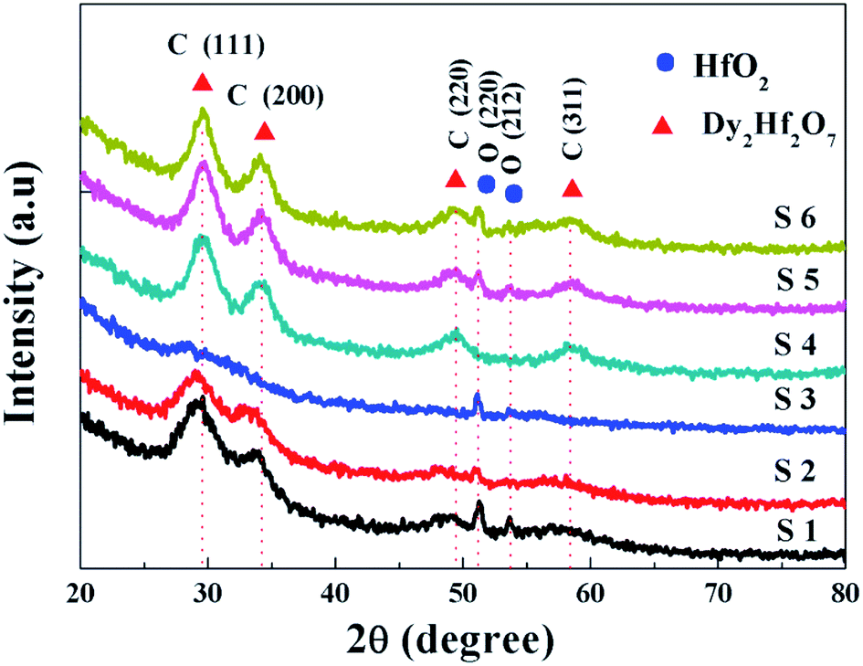
Fig. 1 shows the XRD pattern of the HfDyOx dielectric films as functions of the sputtering power and annealing temperature by matching with Dy2Hf2O7 (JCPDS card no. 24-0360) and HfO2 (JCPDS card no. 21-0904). It can be clearly noted that the diffraction peaks located at 29.6°, 34.3°, 49.4° and 58.6° correspond to the (111), (200), (220), and (311) plane of the cubic Dy2Hf2O7, respectively. The main diffraction peaks located at 51.28° and 53.78° can be attributed to the (220) and (212) plane of HfO2 with orthorhombic phases, respectively. As shown in Fig. 1, as the sputtering power of the Dy target increases from 5 to 15 W, a reduced intensity of the diffraction peaks and an increased full width at a half maximum were observed. Furthermore, as the sputtering power is increased to 15 W, it was clearly observed that all of the cubic-structured peaks disappear. As we know, the HfDyOx gate dielectric films with a cubic phase can contribute to reducing the trap charge density, decreasing the gate leakage current and increasing the dielectric constant.15 Therefore, it can be concluded that the appearance of the cubic phase HfDyOx will lead to a decreased dielectric constant and an increased leakage current in the S3 sample compared with the S2 sample, which is not beneficial for improving the electrical performance. The increase in disorder in the S3 sample could be due to the increased Dy doping concentration and the reduced oxygen content in the target films. Combined with the above described analysis results, 10 W-deposited HfDyOx gate dielectric thin films have been chosen and used to further explore the effect of different annealing temperatures on the interfacial chemistry and electrical characteristics of HfDyOx dielectric films. Considering the S2, S4, S5 and S6 samples, when the annealing temperature of the S2 sample was increased from 400 to 600 °C, it can be seen that the diffraction peaks shift slightly towards a higher angle, which could be due to the increased lattice constant. This can be explained by the fact that a larger ionic radius of dysprosium (91 pm) than that of hafnium (71 pm) results in the increase in the lattice constant, which will be confirmed by the following XPS measurements. In addition, with the increasing annealing temperature, the increased peaks intensities and the decreased full width at half maximum for all of the diffraction peaks have been detected, which is primarily due to the increasing inter-diffusion of hafnium, dysprosium and oxygen, resulting in an enhanced order of grain arrangement.16 Furthermore, the enhanced crystallinity will bring about a reduction in the number of trapping centers and carrier scattering events, which facilitates the formation of carrier conductive channels within the film, resulting in an increase in the gate leakage current.17
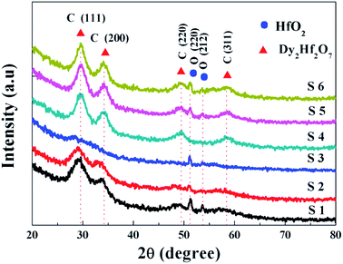 |
| | Fig. 1 XRD patterns of the HfDyOx films for samples S1–S6. | |
3.2 Interface chemical bonding states analysis
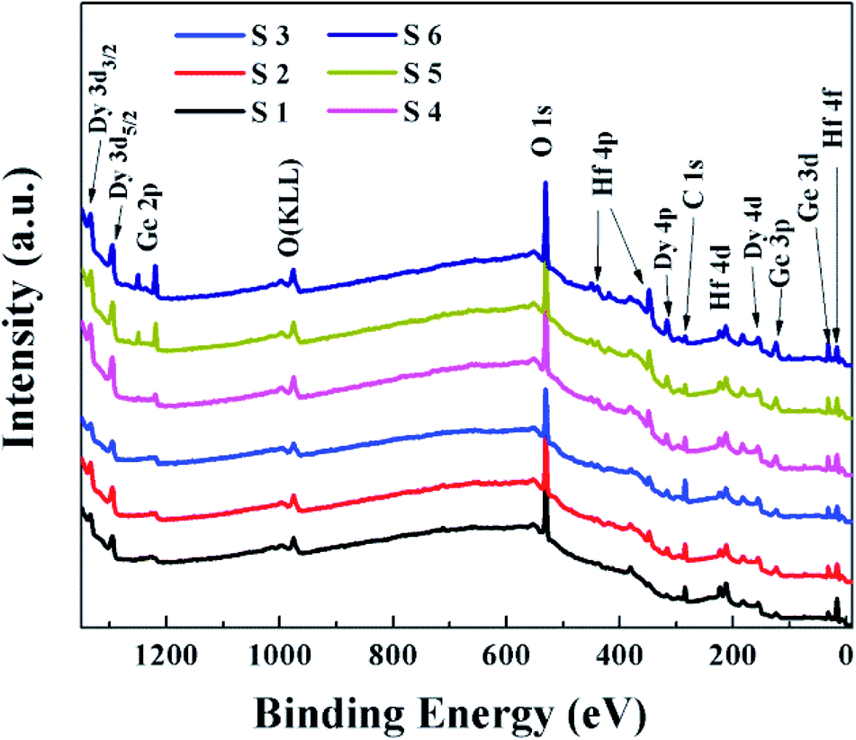
To explore the effect of the dielectric depositional conditions on the interfacial chemical bonding states, the ex situ XPS of the HfDyOx films were measured. All of the XPS measured data were fitted through the Gaussian and Lorentzian functions to achieve Shirley background subtraction. Fig. 2 shows that the survey spectra of the HfDyOx/Ge gate stacks, including the Ge, O, Hf, Dy and C elements, which demonstrates the successful preparation of the HfDyOx films. In addition, all of the measurement data were calibrated using the binding energy peak (284.6 eV) of C 1s. The presence of a small amount of C elements can be attributed to the contamination introduced during the measurement.
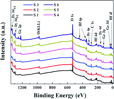 |
| | Fig. 2 XPS survey spectra for samples S1–S6. | |
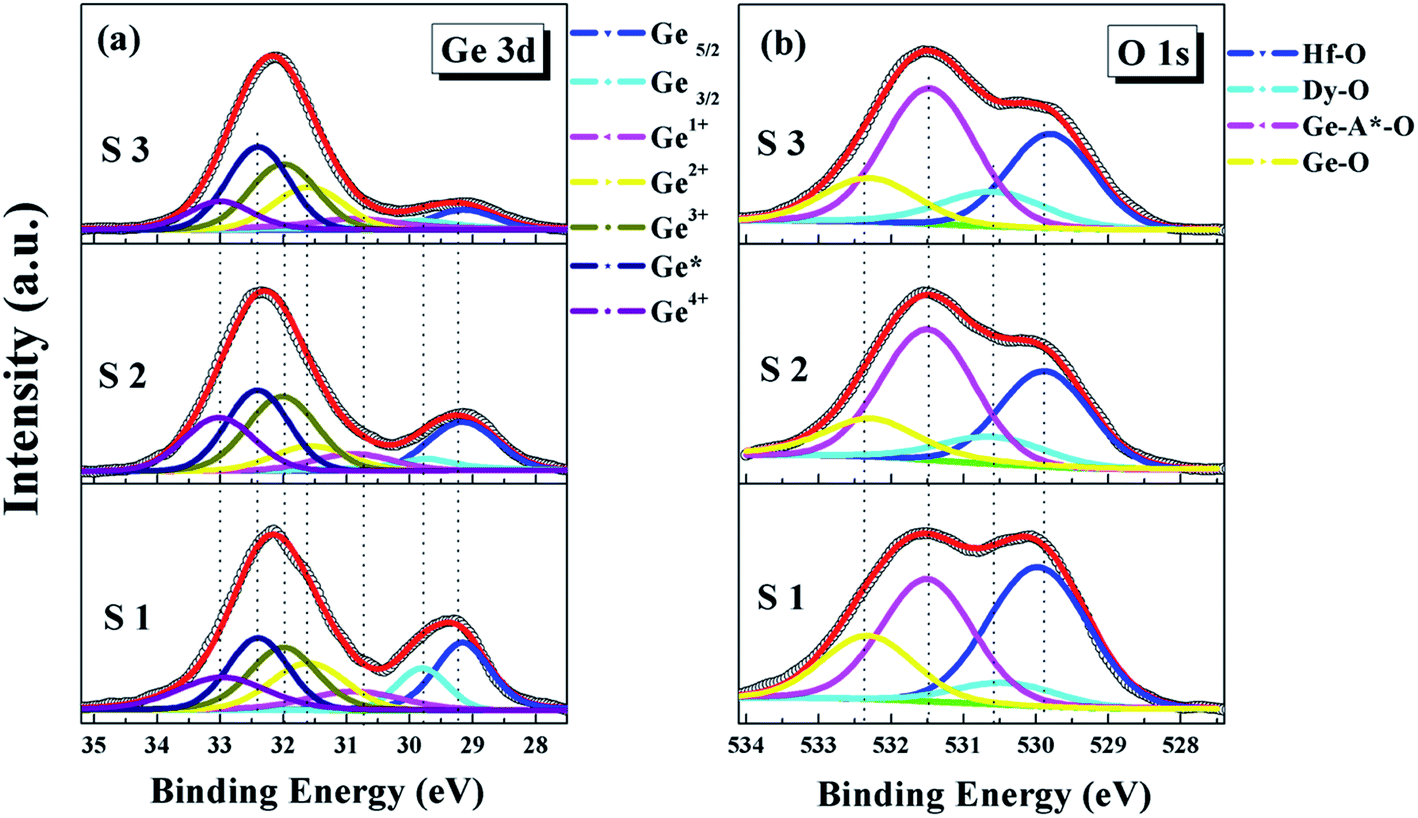
Fig. 3a and 4a show the high-resolution Ge 3d XPS spectra of all of the samples and the quantified XPS results are summarized in Table 1. Furthermore, all of the Ge 3d spectra are convoluted into three chemical components, corresponding to Ge0, Ge–O (Ge1+, Ge2+, Ge3+ and Ge4+) and germanate (Ge*), respectively. Herein, the bonding state of Ge* was found between the Ge3+ and Ge4+ components.18 The interfacial layer of the HfDyOx/Ge gate stacks contain all of the Ge oxides (Ge1+, Ge2+, Ge3+ and Ge4+). Compared to the Ge oxides (Ge1+ and Ge3+), an increase in the content of GeO (Ge2+) and GeO2 (Ge4+) tends to cause a sharp degradation of the device performance. Owing to the fact that Ge2+ and Ge4+ have a higher thermal instability than Ge1+ and Ge3+. Fig. 3a displays the Ge 3d spectra for the S1, S2, and S3 samples. Compared to S1 sample, a slight reduction in the Ge sub-oxides and a slight increase in germanate were observed in the S2 sample. This indicates that the higher sputtering power of the Dy metal target could be conducive to the consumption of unstable Ge oxides on the interface. In combination with Table 1, it can be noted that the Ge3+ content increases and the Ge4+ content decreases. This could be due to the following chemical reaction:
| | |
2GeO2 + Dy → GeDyO + Ge2O3
| (2) |
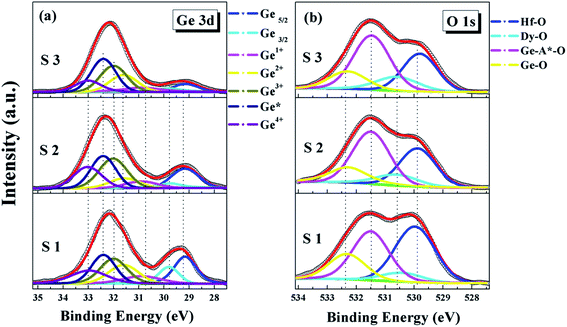 |
| | Fig. 3 (a) Ge 3d and (b) O 1s XPS core-level spectra for samples S1–S3. | |
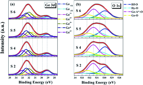 |
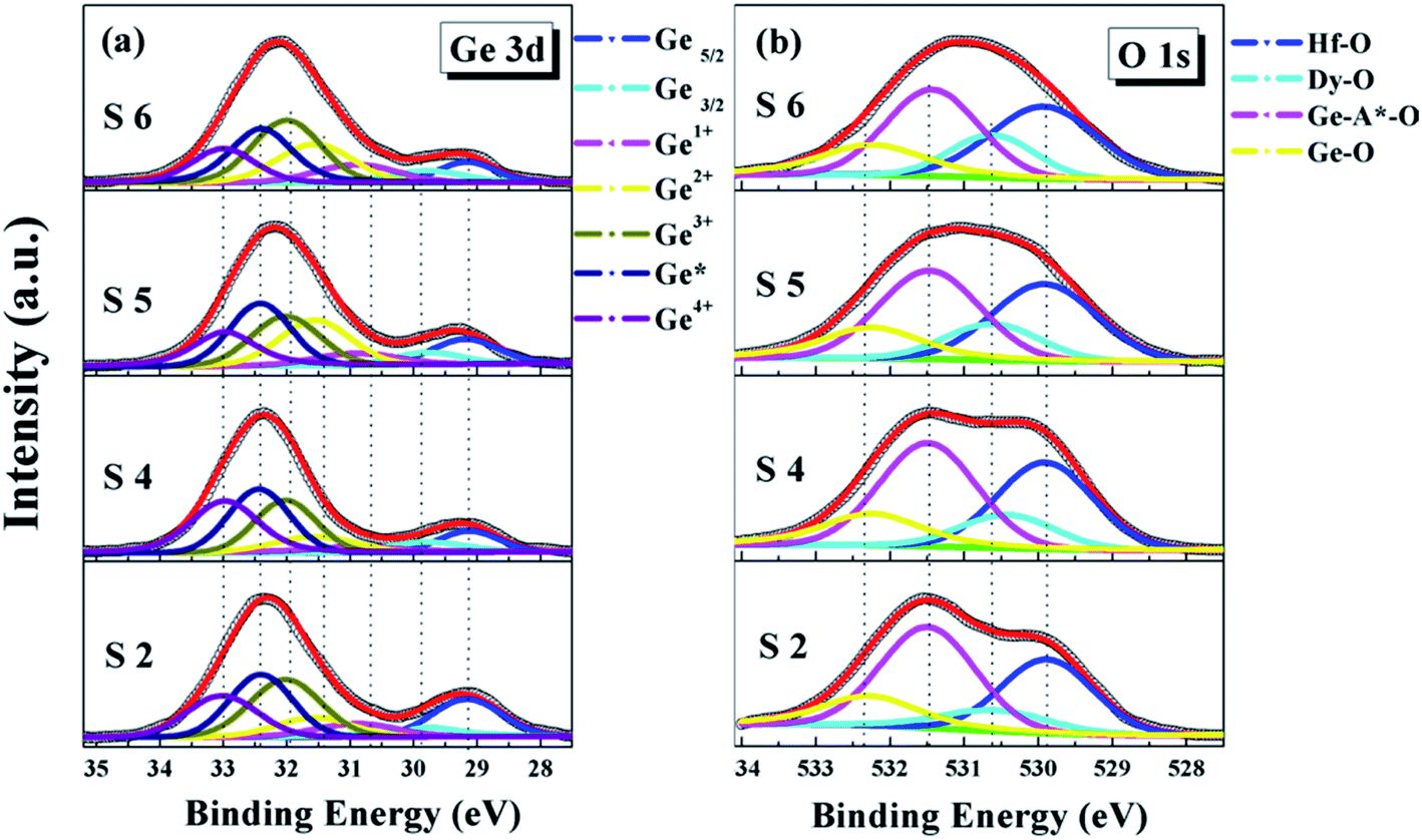
| | Fig. 4 (a) Ge 3d and (b) O 1s XPS core-level spectra for samples S2, S4, S5 and S6. | |
Table 1 The peak area percentages of Ge0, Ge1+, Ge2+, Ge3+, Ge4+ and germinate in the Ge 3d core-level XPS spectra for samples S1–S6
| Sample |
Ge0 (%) |
Ge1+ (%) |
Ge2+ (%) |
Ge3+ (%) |
Ge* (%) |
Ge4+ (%) |
| S1 |
26.8 |
8.0 |
14.5 |
19.1 |
18.3 |
13.3 |
| S2 |
20.5 |
6.3 |
8.6 |
24.3 |
23.1 |
17.2 |
| S3 |
17.6 |
5.8 |
16 |
22.1 |
25.3 |
13.2 |
| S4 |
18.6 |
3.0 |
11.8 |
23.4 |
22.2 |
21.0 |
| S5 |
15.0 |
6.2 |
16.3 |
25.2 |
22.1 |
15.2 |
| S6 |
12.5 |
8.6 |
17.2 |
25.6 |
21.8 |
14.3 |
Similarly, in comparison with the S3 samples, a significant reduction in the intensity of Ge0 and GeO2 and an obvious increase in the Ge sub-oxides and germanate were observed, which could be attributed to the reason that the excessive sputtering power greatly promotes the inter-diffusion of the interface layer and the re-diffusion. Furthermore, the excessive Dy doping results in a relative decrease in the oxygen content of the interface layer, which may be conducive to the occurrence of the following reactions:
| | |
Ge + GeO2 → 2GeO or Ge2O3
| (4) |
| | |
Hf(Dy) + GeO → Hf(Dy)GeO
| (5) |
To further verify the effect of the sputtering power on the interfacial chemistry component, the high-resolution O 1s XPS spectra for the S1–S3 samples is demonstrated in Fig. 3b and the quantified O 1s XPS results are listed in Table 2. All of the O 1s spectra have been deconvoluted into four chemical components, including Hf–O (529.88 eV), Dy–O (530.60 eV), germanate Ge–A*–O (531.49 eV) and Ge–O (532.28 eV), respectively. As demonstrated in Fig. 3b, it can be clearly observed that the intensity of Dy–O increases gradually and the intensity of Hf–O decreases with the sputtering power ranging from 5 to 15 W, indicating that the Dy concentration is increasing in the films. In agreement with the Ge 3d spectra, the increase in germanate and the reduction in the Ge–O content have also been found.
Table 2 The peak area percentages of all the O 1s peaks for samples S1–S6
| Sample |
Hf–O (%) |
Dy–O (%) |
Ge–A*–O (%) |
Ge–O (%) |
| S1 |
38.8 |
5.7 |
37.2 |
18.3 |
| S2 |
34.5 |
10.6 |
38.0 |
16.9 |
| S3 |
28.0 |
13.3 |
44.3 |
14.4 |
| S4 |
33.1 |
12.3 |
37.3 |
17.3 |
| S5 |
32.8 |
13.1 |
37.4 |
16.7 |
| S6 |
33.9 |
14.5 |
35.2 |
16.4 |
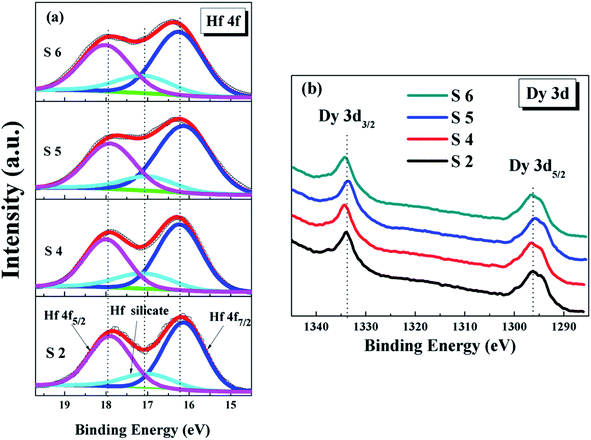
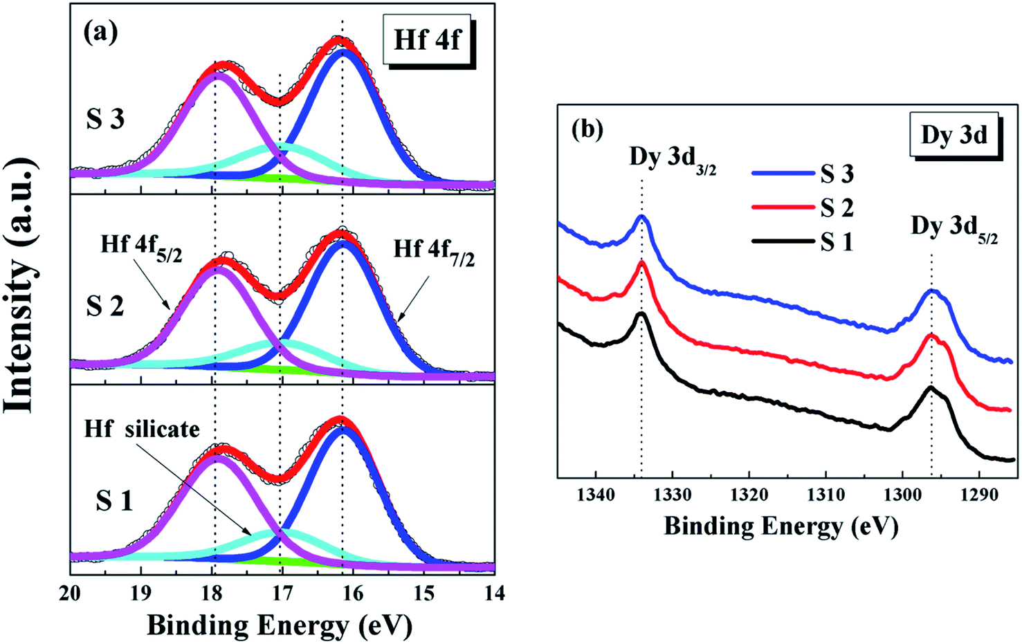
In order to further investigate the composition of the HfDyOx dielectric film, the high-resolution Hf 4f and Dy 3d spectra have also been obtained and are shown in Fig. 5. Owing to the spin–orbit splitting, the Hf 4f spectra are decomposed into three peaks, including a Hf-germanate and two main peaks (Hf 4f7/2 and Hf 4f5/2). The Hf 4f7/2 and Hf 4f5/2 peak are set at 16.13 and 17.9 eV, which is in good agreement with the reported value for HfO2.19 Comparing S1 with the S2 and S3 samples, it is easy to determine that the composition of the Hf-germanate is gradually increasing, which is consistent with previous Ge 3d and O 1s XPS measurement results. Furthermore, the Dy 3d spectra shown in Fig. 5b consists of two peaks of Dy 3d5/2 and Dy 3d3/2, which are attributed to the spin–orbit splitting. No apparent changes in the peak position and only a slight increase in the areas of the peaks were observed, suggesting the Dy content in the HfDyOx thin films increases with the increase in sputtering power. Based on all of the XRD and XPS measurements, the conclusion can be drawn that the controlled composition and the optimized interface chemistry have been achieved in the S2 sample.
 |
| | Fig. 5 (a) Hf 4f and (b) Dy 3d XPS core-level spectra for samples S1–S3. | |
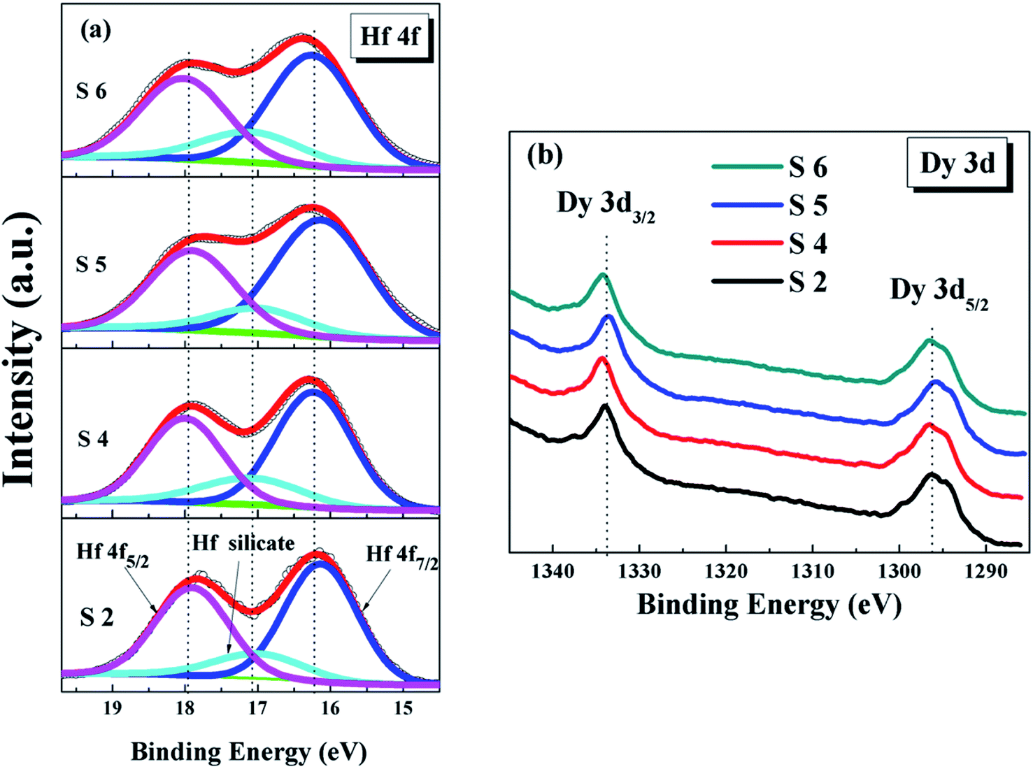
In order to further optimize the interface chemistry and improve the device performance, annealing was performed for the 10 W-driven HfDyOx/Ge gate stacks from 400 to 600 °C, respectively. For the S4–S6 samples, the deposited films selected the S2 sample with a Dy sputtering power of 10 W. A comparative XPS spectra analysis of the S2, S4, S5 and S6 samples is presented in Fig. 4 and 6 and the corresponding calculated components are also displayed in Tables 1 and 2. Based on Fig. 4a, it can be noted that the intensity in Ge0 has decreased with the increasing annealing temperature from 400 to 600 °C, implying that the higher temperature annealing facilitates the Ge re-diffusion in the high-k/Ge interface layers. In addition, comparing the S2 and S4 samples, a significant reduction in the Ge1+ and Ge3+ content and an increase in the Ge2+ and Ge4+ content have been detected, which could be due to the increased oxygen diffusion after annealing. As a result, it can be concluded that the 400 °C-annealed S4 sample displays a degraded interface quality and inevitably leads to further degradation in the electrical performance such as an unacceptable flat band voltage and generation of hysteresis. However, as the annealing temperature continues to increase, there is an increasing trend for the Ge1+, Ge2+ and Ge3+ content and a decreasing trend for the Ge4+ content, indicating that higher temperature annealing favors an increase in the interface stability. In combination with Table 1, it can be further observed that the germanate continues to decrease with the increasing annealing temperature. This could be due to the increased packing density of the dielectric films with the increase in the annealing temperature, which hinders inter-diffusion and Ge re-diffusion to some extent. Finally, there is a continuous slight increment in the total amount of Hf–O and Dy–O content listed in Table 1, which could be due to the fact that the higher temperature annealing accelerates the oxygen diffusion in the HfDyOx films. In addition, the annealing temperature dependent O 1s core-level spectra of the HfDyOx/Ge gate stacks were also investigated, as demonstrated in Fig. 4b and Table 2. With the increase in the annealing temperature, it can be clearly observed that the content of the Hf–O peak area is decreasing, while the Dy–O peak area is increasing, which may due to different interface dipoles between the dielectric film and the Ge substrate. In the case of the S2 sample, the atomic percentage of Hf:Dy is estimated to be 76:24 based on the Hf–O/Dy–O peak-area ratio, which is equivalent to the mole fraction of (HfO2)0.76(Dy2O3)0.24. When the annealing temperature is increased to 600 °C, the content of both tends to be in the equilibrium state. In the case of the dielectrics, the doping amount of Dy in the film is slightly increased as the annealing temperature is increased. The reason for this is that the components are sufficiently fused to each other at higher temperatures. This could lead to an increase in the density and crystallinity of the films. Of course, this fusion is limited owing to the limited Hf and Dy content, which is shown to be essentially flat when the temperature is increased to 600 °C. In addition, in combination with Table 2, it can be further observed that the germanate content continues to decrease and the Ge–O content increases slightly with the increase in the annealing temperature. This is consistent with the results of the previous XRD analysis. The corresponding Hf 4f and Dy 3d XPS spectra are shown in Fig. 6. As shown in Fig. 6a, it can be seen that the Hf-germanate decreases gradually from the S2 to the S6 sample. From Fig. 6b, a tendency to shift towards low binding energy can be observed for the Dy 3d spectra, indicating the full oxidation of the HfDyOx films after the higher-temperature-induced oxygen diffusion. To explain the evolution of the interface chemistry related to the annealing temperature, the exact mechanism is summarized and displayed in two different reaction processes in the high-k/Ge interface.
 |
| | Fig. 6 (a) Hf 4f and (b) Dy 3d XPS core-level spectra for samples S2, S4, S5 and S6. | |
The oxide growth process, following the reaction, results in the generation of the GeOx layer.
| | |
Ge + O → GeO or GeO + O → GeO2
| (6) |
Another process is the oxide desorption process through the following reaction:
| | |
Hf(Dy) + O + Ge → Hf(Dy)GeO or Hf(Dy) + GeO
| (7) |
The desorption of the volatile products, such as GeO and Hf(Dy)GeO, can occur at temperatures of less than 390 °C,20 which tends to hinder the growth of the interfacial layer. Therefore, it can be inferred that with the increase in the annealing temperature the oxide desorption process is better than the oxide growth process, which explains why the annealing process does not result in an optimized interface layer.
3.3 Band alignment characterization
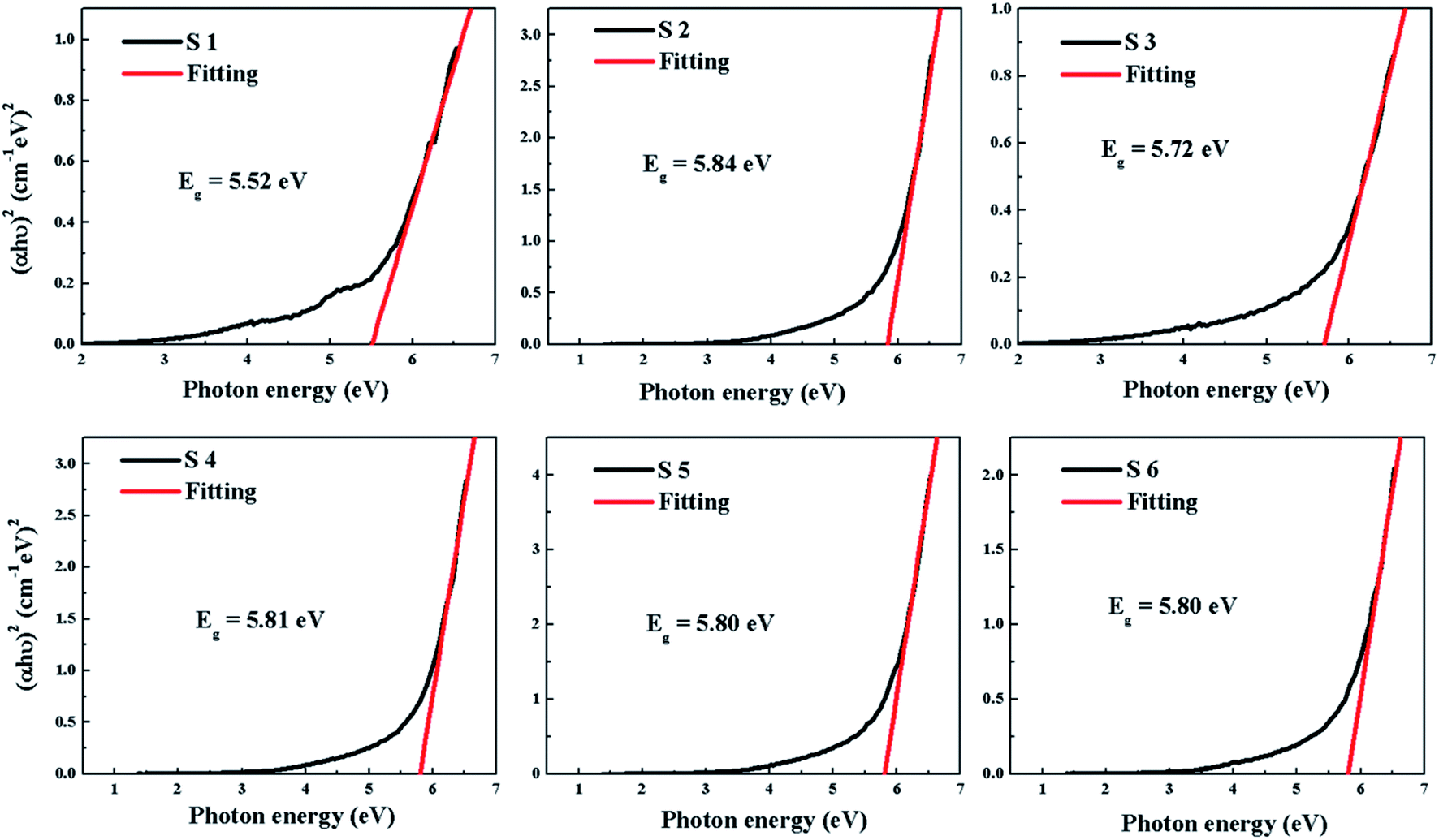
The transmittance and absorption spectra of the HfDyOx films deposited on quartz glass wafers were explored using UV-Vis spectroscopy. Fig. 7 shows the transmittance spectrum of all of the HfDyOx films. It can be clearly observed that the transmittance of all of the samples is more than 90% in the visible light region, indicating that all of the samples have a high transmittance and there is great potential application in transparent semiconductor devices. In the past few years, transparent electronic products have been highly regarded, therefore HfDyOx dielectric films can be used as one of the most promising materials for next-generation flat panel displays, owing to the high transmittance and excellent electrical properties. Furthermore, it is well known that the energy band gap Eg of the dielectric film can be inferred based on the obtained absorption spectra. As we know, HfDyOx is a direct band gap insulator and the optical energy band gap (Eg) can be obtained by plotting (αhν)2 versus (hν), as shown in Fig. 8. Comparing sample S1 with S2, it can be seen that the Eg of the HfDyOx films results in an acceptable shift ranging from 5.52 to 5.84 eV with the increase in the Dy doping content. The increase in Eg can be attributed to the fact that the appropriate increase in the Dy doping content facilitates the reduction of oxygen vacancies in the dielectric film and compensates for the oxidation charge defect of the film. Correspondingly, the defects in the dielectric film are mainly oxygen vacancies, therefore its reduction implies the increase in the energy band gap.21 However, comparing sample S2 with S3, it has been observed that a reduction in Eg is detected when continuing to increase the Dy doping concentration, which can be attributed to the smaller Eg for Dy2O3 (∼4.8 eV).22 In the case of the 10 W-deposited film, with an increase in the annealing temperature, the Eg of the HfDyOx films is maintained at about 5.80 eV and no substantial shift was observed.
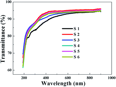 |
| | Fig. 7 Transmittance spectra of the HfDyOx films for samples S1–S6. | |
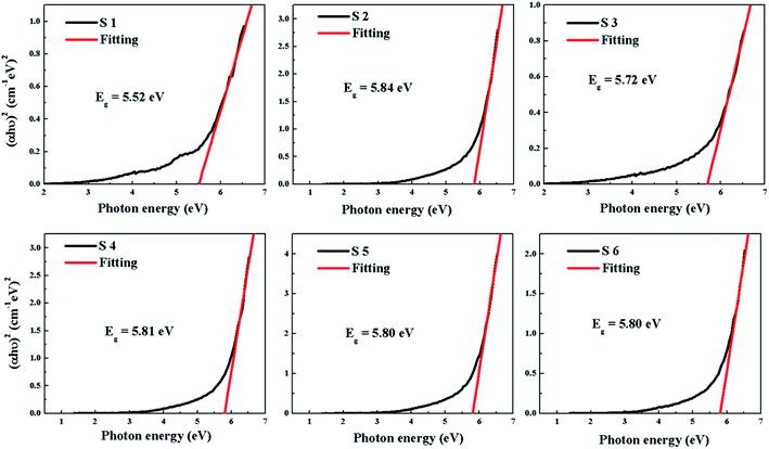 |
| | Fig. 8 The band gap of the HfDyOx films for samples S1–S6. | |
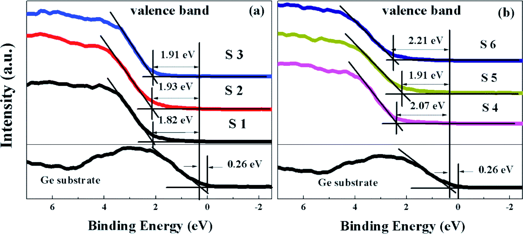
Considering the power consumption of the device, obtaining a small gate leakage current is the key. A sufficient injection barrier can be effective for limiting the gate leakage current, which implies that the band offsets are certainly more than 1 eV. It is generally known that the band offset is the difference between the valence band maximum (VBM) and the conduction band minimum (CBM). Therefore, the valence band maximum differentials between the HfDyOx films and the Ge substrates can be written as:
| | |
ΔEv(HfDyOx–Ge) = Ev(HfDyOx) − Ev(Ge)
| (8) |
As highlighted in Fig. 9, the valence band edge (Ev) is measured using the linear epitaxial method. It can be seen that the extrapolated valence band edge of Ge is 0.26 eV, and the valence band offsets (ΔEv) between the HfDyOx dielectric films and the Ge substrates were calculated to be 1.82, 1.93, 1.91, 2.07, 1.91, and 2.21 eV, respectively, corresponding to the S1–S6 samples. On the basis of Kraut's method,22 the valence-band alignment of the dielectric films can be extrapolated by combining the ΔEv values and the band gap of the HfDyOx films and Ge, the conduction band offset ΔEc can be described using the following formula:
| | |
ΔEc(HfDyOx–Ge) = Eg(HfDyOx) − ΔEv(HfDyOx–Ge) − Eg(Ge)
| (9) |
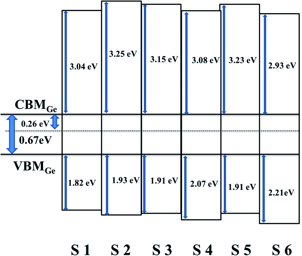
Here, the energy gap of the Ge substrate is 0.67 eV. As highlighted in
Fig. 10, the Δ
Ec values for the S1–S6 samples were determined to be 3.04, 3.25, 3.15, 3.08, 3.23 and 2.93 eV, respectively, indicating that the barrier height of all of the HfDyO
x/Ge gate stacks is more than 1 eV. Considering that the Δ
Ec is closely related to the tunneling leakage current, the high Δ
Ec indicates a small leakage current to a certain extent.
23 Based on
Fig. 10, it can be noted that the optimized Δ
Ev of 3.25 eV for the S2 sample demonstrates potential application as a high-
k gate dielectric in Ge-based MOS devices. It was also found that the S2 sample has the smallest leakage current, which is discussed in the following section.
 |
| | Fig. 9 The difference between the VBM for (a) samples S1–S3 and (b) samples S4–S6. | |
 |
| | Fig. 10 Schematic band diagrams for samples S1–S6. | |
3.4 Electrical performance characterization of the Ge-MOS device
3.4.1 C–V characteristics. The C–V characteristic curves of all of the samples undergoing different deposition conditions and annealing temperatures are shown in Fig. 11. All of the extracted electrical performance parameters are summarized in Table 3. As exhibited in Fig. 11a, the high frequency (1 MHz) C–V characteristics for the S1–S3 samples were measured using the double sweep forward and backward from reverse method with the gate voltage. It can be clearly seen that the saturation capacitance (Cox) in the accumulation region does not display a linear increase with the increase in the sputtering power. The trend of increasing first and then decreasing was observed, indicating that the dielectric constant first increases and then decreases. In addition, it can also be noted that only the S2 sample displays an obvious saturation zone, depletion zone and inversion zone. This implies achievement of an effective unpinning Fermi level. This can be mainly attributed to the optimized interface quality and the reduced oxygen vacancy in the dielectric film. However, compared to the S2 sample, the S3 sample displays a degraded electrical performance, including the negative Vfb (−0.6 V), an increased hysteresis value (−0.06 V), and a reduced Cox, as presented in Table 1. This could be due to the excessive Dy doping which introduces the formation of the germanate and low-valence Ge ions in the interface layer. Furthermore, the generation of germanate and low-valence Ge oxides will generate a Fermi-level pinning effect,24 resulting in the degraded electrical properties. To investigate the effect of annealing temperature on the HfDyOx/Ge MOS capacitors, the C–V characteristics for S2–S6 samples are shown in Fig. 11c. Compared to the S2 sample without annealing, it can be clearly seen that the S4 sample with 400 °C annealing has a significant positive Vfb (0.3 V), an unacceptable hysteresis value (−0.12 V) and a minimal Cox. The S5 and S6 samples, corresponding to 500 and 600 °C annealing, also have a negligible negative Vfb and hysteresis value. This could be attributed to the Ge re-diffusion on the interface leading to the formation of large amounts of Ge oxide. This is also clearly demonstrated in the XPS analysis described above. Furthermore, the reason for the sharp decline in the electrical properties of the S4 sample may be due to the distinct increase in unstable low-valence Ge ions (Ge2+ and Ge4+) in the interfacial layer. Furthermore, in the case of the S2 sample, the reduced value of Vfb could be attributed to the introduction of a reduced positive charge and/or a captured negative charge by appropriately increasing the Dy doping. At the same time, a vanishing hysteresis could be due to a decrease in the interfacial state and the improvement of trap behavior.
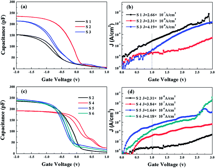 |
| | Fig. 11 (a) Capacitance–voltage (C–V) characteristics for samples S1–S3. (b) Leakage current density–voltage (J–V) characteristics for samples S1–S3. (c) Capacitance–voltage (C–V) characteristics for samples S2, S4, S5 and S6. (d) Leakage current density–voltage (J–V) characteristics for samples S2, S4, S5 and S6. | |
Table 3 Parameters of the S1–S6 MOS capacitors extracted from the C–V and J–V curves
| Sample |
EOT (nm) |
k |
Vfb (V) |
ΔVfb (V) |
Qox (cm−2) |
Nbt (cm−2) |
J (A cm−2) |
| S1 |
6.17 |
9.47 |
−0.57 |
−0.17 |
1.80 × 10¹² |
5.11 × 10¹¹ |
2.66 × 10⁻⁷ |
| S2 |
2.46 |
22.4 |
0.07 |
— |
−1.87 × 10¹¹ |
— |
2.31 × 10⁻⁸ |
| S3 |
3.06 |
19.09 |
−0.6 |
−0.06 |
2.68 × 10¹² |
2.56 × 10¹¹ |
4.19 × 10⁻⁸ |
| S4 |
3.67 |
15.92 |
0.3 |
−0.12 |
−1.02 × 10¹² |
4.56 × 10¹¹ |
3.84 × 10⁻⁷ |
| S5 |
2.43 |
21.72 |
−0.11 |
−0.09 |
6.83 × 10¹¹ |
4.39 × 10¹¹ |
1.64 × 10⁻⁶ |
| S6 |
2.52 |
20.92 |
−0.15 |
−0.07 |
8.60 × 10¹¹ |
3.34 × 10¹¹ |
4.18 × 10⁻⁶ |
In addition, combined with the Vfb, ΔVfb and Cox, the other essential electrical parameters can be extracted, including the permittivity (K), the oxide-charge density (Qox), the border trapped oxide charge density (Nbt) and the EOT of the HfDyOx/Ge gate stacks, as listed in Table 3, respectively. As demonstrated in Table 3, the EOT value was confirmed to be 6.17, 2.46, 3.06, 3.67, 2.43 and 2.52 nm, corresponding to the S1–S6 samples, respectively. It can be easily found that the S2 sample processes a thinner EOT, indicating a larger K value caused by the optimized interfacial layer and a high quality dielectric film. After annealing, no satisfactory reduction in EOT values was observed, which indicates that annealing has no obvious suppression effect on the growth of the interfacial layer. Combined with the extracted electrical parameters, it can be noted that the S2 sample has diminished negative oxide-charge density, meaning the least amount of oxygen vacancies in the high-k dielectrics. For the S3 sample, it can be observed that the increased Qox and Nbt is caused by the existing and the addition of further trapped positive oxide charges or positive charges in the interfacial layer. This can also be confirmed by the fact that the excess Dy doping can facilitate the inter-diffusion and the Ge re-diffusion.25–27 As exhibited in Table 3, an increase in the Qox and Nbt has been observed for the annealed HfDyOx/Ge gate stacks, indicating the degraded interface chemistry and the increased gate leakage current.
3.4.2 J–V characteristics and current conduction mechanisms. The typical J–V characteristic curves of all of the devices can be found using the HfDyOx/Ge MOS capacitors, as exhibited in Fig. 11b and d. For the S1–S3 samples, when the gate voltage is set at 1 V, the gate-leakage-current–density is determined to be about 2.66 × 10⁻⁷, 2.31 × 10⁻⁸ and 4.19 × 10⁻⁸ A cm−2, respectively, as shown in Fig. 11b. It is clearly shown that the gate leakage current density has a tendency to first decrease and then increase with the increasing Dy doping concentration. This can be primarily attributed to the fact that the appropriate Dy-doping content in the HfDyOx films can reduce the dangling bonds and inhibit the trapping charge on the interfacial layer, resulting in a suppressed leakage current. As displayed in Fig. 11d, the gate-leakage-current–density is determined to be about 3.84 × 10⁻⁷, 1.64 × 10⁻⁶ and 4.18 × 10⁻⁶ A cm−2 at 1 V, respectively, corresponding to 400, 500 and 600 °C-annealed samples. Compared to the S2 sample, the leakage current after annealing has increased to some extent owing to the degraded interface quality. As a result, it can be concluded that the S2 sample without thermal treatment demonstrates an optimized electrical performance, implying that the suitable rare-earth-doping HfO2 possesses an optimized interfacial quality and an excellent dielectric performance.In this work, the J–V characteristics of all devices were derived from the electrons tunneling from the semiconductor (Ge) to the metal (Al), resulting in different tunneling mechanisms by applying a positive voltage in the Al/HfDyOx/Ge MOS capacitor. To study the influence of the Dy-doping and annealing on the carrier conduction mechanisms for the corresponding capacitors, some leakage current conduction mechanisms (CCMs) have been thoroughly analyzed. Fig. 11b and d depicts the J–V curves of different amounts of Dy-doping and the annealing temperature dependent samples and an increase in the tunneling current density has been observed with the increased gate voltage. This could be attributed to the transformation of the CCMs at various tunneling regions, including the Schottky emission (SE), Poole–Frenkel (PF) emission and Fowler–Nordheim (FN) tunneling.28 In order to investigate the influence of different doping contents and annealing temperatures on the CCMs of the Al/HfDyOx/Ge capacitors under substrate injection, several CCMs were systematically analyzed and evaluated.
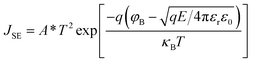
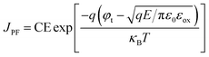
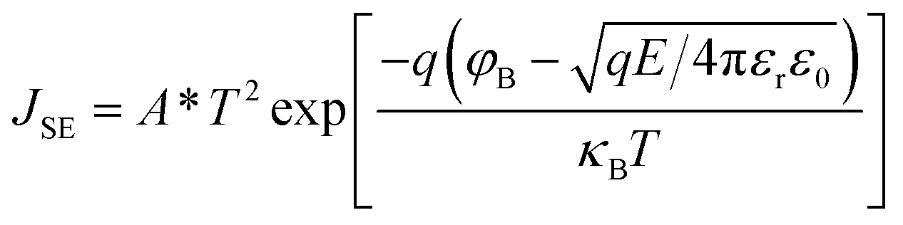
The occurrence of the SE mechanism is caused by the thermal excitation charge, which obtains sufficient energy and then passes through the interface barrier from the gate electrode or semiconductor substrate to the dielectric. The PF emission mechanism can be attributed to the thermally excited electrons that have either been captured or emitted from the traps and have entered the conduction band of the dielectrics to form the gate leakage current. Under a high electric field, the carriers will tunnel through the insulator, that is, electrons are injected into the conduction band of the oxide through the triangular barrier, the dominant CCMs are governed by FN tunneling. All of the mechanisms from the SE emission, PF emission, and FN tunneling can be expressed using the following formulas:29–31
| |
 | (10) |
| |
 | (11) |
| |
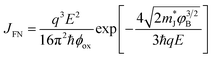 | (12) |
In which
A* is the effective Richardson constant,
κB and
φB are the Boltzmann constant and the Schottky barrier height,
φt is the trap energy level,
ε0 and
εr are the vacuum dielectric constant and the optical dielectric constant,
mT* is the tunneling effective mass of the gate dielectric film, and the electric field can be stated as
E = (
V −
Vfb)/
tox, respectively.
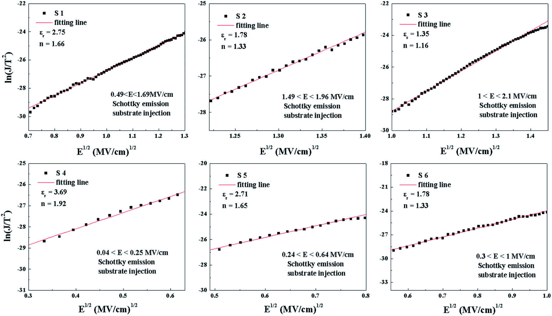
Fig. 12 shows the good linear behavior of ln(
J/
T2)
versus E1/2 in the low electric field region, indicating that the dominant CCMs may conform with the SE emission under substrate injection. In addition, based on the linear fitting lines
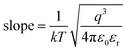
, the optical dielectric constant
εr and the refractive index
n =
εr1/2 can be extracted and are exhibited in
Fig. 12.
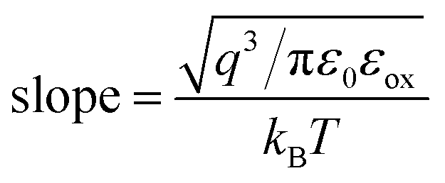
32,33 It can be noted that the values of
εr and
n have been calculated to be (2.75, 1.66), (1.78, 1.33), (1.35, 1.16), (3.69, 1.92), (2.71, 1.65) and (1.78, 1.33), corresponding to samples S1–S6, respectively. The
n values of S2, S3 and S5 deviate from the theoretical value of 2.1 and the experimental value of 1.6–1.9 in previous reports,
34,35 which means that only the current conduction mechanism (CCM) of the S1, S4 and S6 samples satisfies the SE mechanism at a lower electric field.
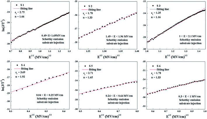 |
| | Fig. 12 The SE emission mechanism: ln(J/T2) versus E1/2 plots for samples S1–S6. | |
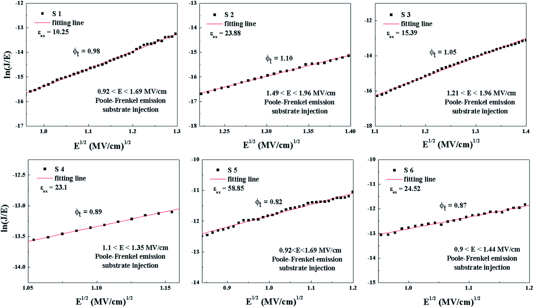
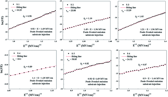
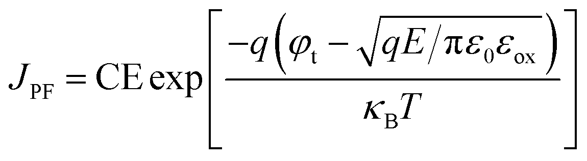
The plots of ln(J/E2) versus E1/2 for the S1–S6 samples are demonstrated in Fig. 13. According to the linear fitting lines , the values of the dielectric constant εox can be extracted and are exhibited in Fig. 13. It can be easily seen that the PF emission becomes dominant as CCMs exist in the corresponding samples at different electric field. The values of εox have been calculated to be 10.25, 23.88, 15.39, 23.1, 58.85 and 24.52, corresponding to the S1–S6 samples, respectively. As the εox value of the S5 sample deviates from the measured value, this indicates that the S5 sample is not governed by the PF emission at 0.92 < E < 1.69 MV cm−1. The trap energy levels (φt) in the HfDyOx thin films are analyzed by the intercept of the red fitting linear plots:
 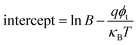 and are highlighted in Fig. 13, which is in good agreement with our previous investigation.36
 |
| | Fig. 13 The PF tunneling mechanism: ln(J/E) versus E1/2 plots for samples S1–S6. | |
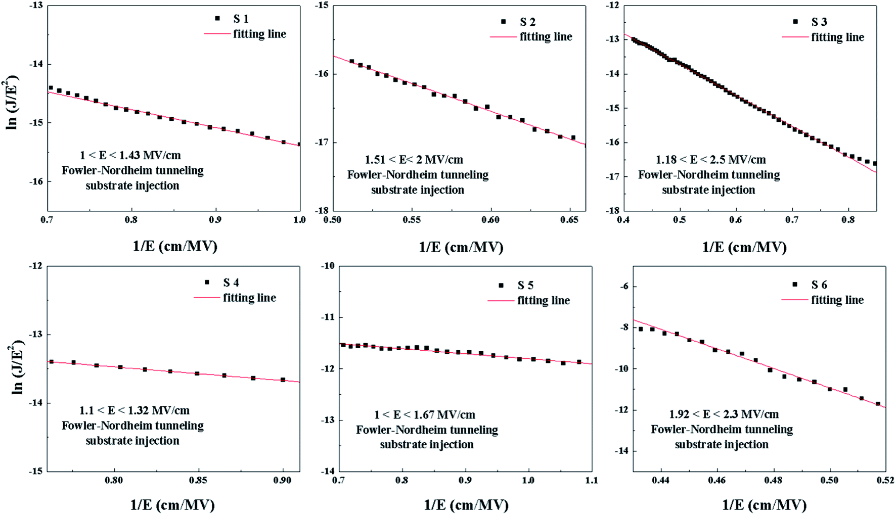
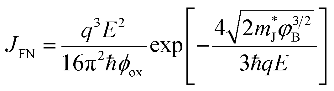
In the FN model, ln(J/E2) and 1/E conform to the linear relationship. Fig. 14 shows ln(J/E2) versus 1/E under substrate injection. It can be seen that the CCMs in the higher electric region appears to follow the FN model under substrate injection. Based on the CCMs analysis, it can be inferred that the dominant CCMs evolve from SE emission, PF emission to FN tunneling with an increase in the electric field.
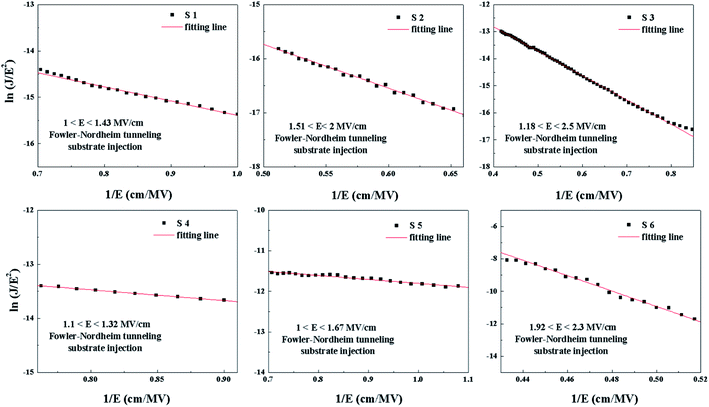 |
| | Fig. 14 The FN tunneling mechanism: ln(J/E2) versus 1/E plots for samples S1–S6. | |
4. Conclusions
In this work, the effects of different deposition and annealing conditions on the interface chemistry and electrical properties of TMA-passivated HfDyOx/Ge gate stacks have been investigated systematically. The evolution of the microstructural, interfacial chemistry, and electrical properties of sputtering-driven HfDyOx gate dielectrics have been investigated using XRD, XPS, and detailed electrical measurements. XRD analyses have confirmed that the crystallinity of the sputtering-deposited HfDyOx dielectric films depends on the sputtering power and the annealing temperature. Characterization via XPS has revealed that 10 W-driven dielectrics demonstrate excellent interface characteristics. This is mainly attributed to the substantial reduction of unstable Ge oxides and the sufficient substitution of Ge for oxygen vacancies in the dielectric films. However, in view of the experimental results, the annealing treatments result in interface performance degradation. Electrical measurements based on a 10 W-deposited HfDyOx/Ge capacitor without annealing exhibit optimized electrical parameters, such as a larger permittivity of 22.4, a smaller flat band voltage of 0.07 V, negligible hysteresis, a lower oxide charge density of ∼1011 cm−2, and the lowest leakage current density of 2.31 × 10⁻⁸ A cm−2. The doping concentration and annealing temperature dependent CCMs in HfDyOx/Ge devices have been investigated and it was revealed that the dominant CCMs evolve from SE emission to PF emission to FN tunneling with an increase in the electric field. As a result, it can be concluded that 10 W-deposited HfDyOx gate dielectrics demonstrate satisfactory interface quality and improved electrical performance, indicating their potential application for use in Ge-based MOSFET devices.
Conflicts of interest
The authors declare no conflicts of interest.
Acknowledgements
The authors acknowledge support from the National Natural Science Foundation of China (11774001, 51572002, 51872186), and the open fund for Discipline Construction, Institute of Physical Science and Information Technology, Anhui University (S01003101).
References
- G. Vellianitis, Z. M. Rittersma and J. Pétry, Appl. Phys. Lett., 2006, 89, 092902 CrossRef.
- G. He, Z. Q. Sun, M. Liu and L. D. Zhang, Appl. Phys. Lett., 2010, 97, 192902 CrossRef.
- R. Shahinur and E. K. Evangelou, IEEE Trans. Electron Devices, 2011, 58, 3549–3557 Search PubMed.
- Y. Huang, J. P. Xu, L. Liu, P. T. Lai and W. M. Tang, Appl. Phys. Lett., 2016, 109, 193504 CrossRef.
- N. Lu, W. Bai, A. Ramirez, C. Mouli, A. Ritenour, M. L. Lee, D. Antoniadis and D. L. Kwong, Appl. Phys. Lett., 2005, 87, 51922 CrossRef.
- F. Bellenger, M. Houssa, A. Delabie, V. Afanasiev, T. Conard, M. Caymax, M. Meuris, K. D. Meyer and M. M. Heyns, J. Electrochem. Soc., 2008, 155, G33–G38 CrossRef CAS.
- H. S. Jung, H. K. Kim, I. H. Yu, S. Y. Lee, J. Lee, J. Park, J. H. Jang, S. H. Jeon, Y. J. Chung, D. Y. Cho, N. I. Lee, T. J. Park, J. H. Choi and C. S. Hwang, J. Electrochem. Soc., 2012, 159, G33–G39 CrossRef CAS.
- Q. Xie, S. Deng, M. Schaekers, D. Lin, M. Caymax, A. Delabie, X. P. Qu, Y. L. Jiang, D. Deduytsche and C. Detavernier, Semicond. Sci. Technol., 2012, 27, 074012 CrossRef.
- D. Bodlaki, H. Yamamoto, D. Waldeck and E. Borguet, Surf. Sci., 2003, 543, 63–74 CrossRef CAS.
- M. M. Frank, S. J. Koester, M. Copel, J. A. Ott, V. K. Paruchuri, H. Shang and R. Loesing, Appl. Phys. Lett., 2006, 89, 112905 CrossRef.
- H. Seo, K. B. Chung, J. P. Long and G. Lucovsky, J. Electrochem. Soc., 2009, 156, H813–H817 CrossRef CAS.
- I. K. Oh, K. Kangsik, Z. Lee, J. G. Song, C. W. Lee, D. Thompson, H. R. Lee, W. H. Kim, W. J. Maeng and H. Kim, J. Mater. Chem., 2015, 3, 4852–4858 CAS.
- J. Gao, G. He, S. Liang, D. Wang and B. Yang, J. Mater. Chem. C, 2018, 6, 2546–2555 RSC.
- M. Modreanu, J. Sancho-Parramon, O. Durand, B. Servet, M. Stchakovsky, C. Eypert, C. Naudin, A. Knowles, F. Bridou and M. F. Ravet, Appl. Surf. Sci., 2006, 253, 328–334 CrossRef CAS.
- J. G. Simmons, J. Phys. D: Appl. Phys., 1971, 4, 613–657 CrossRef CAS.
- T. M. Pan, W. T. Chang and F. C. Chiu, Appl. Surf. Sci., 2011, 257, 3964–3968 CrossRef CAS.
- D. W. Nam, I. T. Cho, J. H. Lee, E. S. Cho, J. Sohn, S. H. Son and H. I. Kwon, J. Vac. Sci. Technol., 2012, 30, 060605 CrossRef.
- Y. J. Cho, W. J. Lee, C. Y. Kim, M. H. Cho, H. Kim, H. J. Lee, D. W. Moon and H. J. Kang, J. Chem. Phys., 2008, 129, 164117 CrossRef PubMed.
- J. Gao, G. He, Z. B. Fang, J. G. Lv, M. Liu and Z. Q. Sun, J. Alloys Compd., 2017, 695, 2199–2206 CrossRef CAS.
- X. J. Zhang, G. Xue, A. Agarwal, R. Tsu, M. A. Hasan, J. E. Greene and A. Rockett, J. Vac. Sci. Technol., 1993, 11, 2553–2561 CrossRef CAS.
- R. Ma, M. Liu, G. He, M. Fang, G. L. Shang, J. W. Zhang, X. F. Chen, J. Gao, G. T. Fei and L. D. Zhang, J. Alloys Compd., 2015, 646, 310–314 CrossRef CAS.
- E. A. Kraut, R. W. Grant, J. R. Waldrop and S. P. Kowalczyk, Phys. Rev. Lett., 1980, 44, 1620–1622 CrossRef CAS.
- E. K. Liu, B. S. Zhu and J. S. Luo, The physics of semiconductors, Publishing House of Electronic Industrial, Beijing, 2003 Search PubMed.
- M. M. Frank, G. D. Wilk, D. Starodub, T. Gustafsson, E. Garfunkel, Y. J. Chabal, J. Grazul and D. A. Muller, Appl. Phys. Lett., 2005, 86, 152904 CrossRef.
- H. J. Quah, K. Y. Cheong, Z. Hassan and Z. Lockman, J. Mater. Sci.: Mater. Electron., 2011, 22, 583–591 CrossRef CAS.
- A. Dimoulas, D. P. Brunco, S. Ferrari, J. W. Seo, Y. Panayiotatos, A. Sotiropoulos, T. Conard, M. Caymax, S. Spiga, M. Fanciulli, C. Dieker, E. K. Evangelou, S. Galata, M. Houssa and M. M. Heyns, Thin Solid Films, 2007, 515, 6337 CrossRef CAS.
- D. P. Brunco, A. Dimoulas, N. Boukos, M. Houssa, T. Conard, K. Martens, C. Zhao, F. Bellenger, M. Caymax, M. Meuris and M. M. Heyns, J. Appl. Phys., 2007, 102, 024104 CrossRef.
- F. C. Chiu, Adv. Mater. Sci. Eng., 2014, 7, 1–18 Search PubMed.
- S. J. Ding, D. W. Zhang and L. K. Wang, J. Phys. D: Appl. Phys., 2007, 40, 1072–1076 CrossRef CAS.
- A. Paskaleva, A. J. Bauer, M. Lemberger and S. Zucher, J. Appl. Phys., 2004, 95, 5583 CrossRef CAS.
- D. K. Avasthi and G. K. Mehta, Swift Heavy Ions for Materials Engineering and Nanostructuring, Springer Series in Materials Science, 2011, p. 1 Search PubMed.
- C. Licitra, E. Martinez, N. Rochat, T. Veyron, H. Grampeix, M. Gely, J. P. Colonna and G. Molas, AIP Conf. Proc., 2007, 931, 292–296 CrossRef CAS.
- H. P. Zhang, R. X. Jia, Y. Lei, X. Y. Tang, Y. Zhang and Y. Zhang, J. Phys. D: Appl. Phys., 2018, 51, 075104 CrossRef.
- G. He, L. Q. Zhu and M. Liu, Appl. Surf. Sci., 2007, 253, 3413–3418 CrossRef CAS.
- W. J. Bae, M. Trikeriotis, J. Sha, E. L. Schwartz, R. Rodriguez, P. Zimmerman, E. P. Giannelisa and C. K. Ober, J. Mater. Chem., 2010, 20, 5186–5189 RSC.
- D. Wang, G. He, L. Hao, J. Gao and M. Zhang, J. Mater. Chem. C, 2019, 7, 1955–1965 RSC.
|
| This journal is © The Royal Society of Chemistry 2020 |
Click here to see how this site uses Cookies. View our privacy policy here. 
 Open Access Article
 This Open Access Article is licensed under a Creative Commons Attribution-Non Commercial 3.0 Unported Licence
 *ab,
Zebo Fang*c,
Lin Haoa,
Zhaoqi Suna and
Yanmei Liua
*ab,
Zebo Fang*c,
Lin Haoa,
Zhaoqi Suna and
Yanmei Liua


 , the optical dielectric constant εr and the refractive index n = εr1/2 can be extracted and are exhibited in Fig. 12.32,33 It can be noted that the values of εr and n have been calculated to be (2.75, 1.66), (1.78, 1.33), (1.35, 1.16), (3.69, 1.92), (2.71, 1.65) and (1.78, 1.33), corresponding to samples S1–S6, respectively. The n values of S2, S3 and S5 deviate from the theoretical value of 2.1 and the experimental value of 1.6–1.9 in previous reports,34,35 which means that only the current conduction mechanism (CCM) of the S1, S4 and S6 samples satisfies the SE mechanism at a lower electric field.
 , the values of the dielectric constant εox can be extracted and are exhibited in Fig. 13. It can be easily seen that the PF emission becomes dominant as CCMs exist in the corresponding samples at different electric field. The values of εox have been calculated to be 10.25, 23.88, 15.39, 23.1, 58.85 and 24.52, corresponding to the S1–S6 samples, respectively. As the εox value of the S5 sample deviates from the measured value, this indicates that the S5 sample is not governed by the PF emission at 0.92 < E < 1.69 MV cm−1. The trap energy levels (φt) in the HfDyOx thin films are analyzed by the intercept of the red fitting linear plots:
  and are highlighted in Fig. 13, which is in good agreement with our previous investigation.36