
 Open Access Article
 This Open Access Article is licensed under a
 Creative Commons Attribution 3.0 Unported Licence
Carrier-mediated ferromagnetism in two-dimensional PtS2†
Konstantina Iordanidou *a,
Michel Houssab and
Clas Perssona
*a,
Michel Houssab and
Clas Perssona
aCentre for Materials Science and Nanotechnology, Department of Physics, University of Oslo, P.O. Box 1048 Blindern, NO-0316 Oslo, Norway. E-mail: konstantina.iordanidou@smn.uio.no
bDepartment of Physics and Astronomy, University of Leuven, B-3001 Leuven, Belgium
First published on 3rd January 2020
Abstract
Using first principles calculations based on density functional theory, we study the impact of hole doping on the magnetic and electronic properties of two dimensional PtS2. Although 2D PtS2 is intrinsically non-magnetic, a stable ferromagnetic phase is found for a wide range of hole densities, owing to the so-called Stoner instabilities. Besides spontaneous magnetization, half-metallicity is additionally observed. The majority and minority spin states exhibit insulating and metallic nature, respectively, allowing a fully polarized spin transport in 2D PtS2. Lastly, hole doping resulting from substitutional doping is investigated. For As-doped PtS2 shallow spin-polarized states close to the valence band edge are observed, and among all studied group-V dopants, As replacing S, is the most promising one to induce p-type conductivity and a subsequent ferromagnetic order in PtS2.
1. Introduction
Over the past decades, the technological advances yielded to smaller transistors and subsequently to devices integrating an increasing number of them. However, as the physical dimensions of the transistors are scaled down, quantum effects start to dominate the device operation. In particular, transistors with very short channel lengths experience source to drain tunneling currents, i.e., high off-state currents which increase the static power consumption and cause heat dissipation. To overcome such limitations, new materials that can sustain aggressive scaling and/or new technologies should be introduced. The “marriage” of two dimensional materials with spintronics1–3 may bring a revolution in today's transistor technology.To realize spintronic nanodevices the selection of materials is critical. For instance, the spin states should be easily established and conveniently manipulated, whereas long-distance spin transport and efficient spin injection should be achieved. Although various spintronic nanodevices have been realized in the last years, the quest for optimal materials is still an open issue. Remarkably, recent experimental observations revealed a long-range ferromagnetic order in 2D compounds like CrI3 and Cr2Ge2Te6.4,5 In addition, spontaneous magnetization has been predicted in monolayer metal chalcogenides, such as GaS, GaSe and InSe, upon hole doping.6–9 Such magnetization arises from an exchange splitting of the electronic states at the valence band edge, where the density of states exhibits a sharp van Hove singularity, leading to the so-called Stoner instability.
Two dimensional PtS2 is a relatively unexplored member of the transition metal dichalcogenide (TMD) family. Its thermodynamically stable structure consists of one hexagonal metal plane sandwiched between two hexagonal chalcogen planes with an octahedral coordination, forming the so-called 1T phase.10,11 Interestingly, a high mobility of 1107 cm2 V−1 s−1 is theoretically predicted for 2D PtS2, which is larger compared to other well-studied TMDs like MoS2.12 In addition, theoretical investigations reveal a transition from a non-magnetic to a ferromagnetic phase upon hydrogenation, and the magnetic moments mainly arise from the Pt 5d orbitals.13
In this paper, the magnetic and electronic properties of hole-doped 2D PtS2 are studied, using first principles calculations based on density functional theory (DFT). Although 2D PtS2 is intrinsically non-magnetic, a stable ferromagnetic phase is found for a wide range of hole densities. Hole doping resulting from substitutional doping is also investigated.
2. Models and computational methods
First principles calculations of monolayer PtS2 are performed using the spin polarized DFT, as implemented in the Vienna ab initio simulation package (VASP).14,15 The generalized gradient approximation, developed by Perdew, Burke and Ernzerhof (PBE), is used for the exchange correlation functional,16 and long-range van der Waals corrections are applied, using the DFT-D3 Grimme method.17 The projected augmented wave (PAW) pseudopotentials are employed,18 along with a kinetic energy cutoff of 400 eV. The Brillouin zone is sampled by a 4 × 4 × 1 k-point grid for the atomic relaxations, whereas a denser grid is considered for the electronic structure calculations. Note that in order to get well-converged magnetic moments, a grid of 18 × 18 × 1 k-points is adopted. The atomic positions are optimized using the conjugate gradient method, with 10−2 eV Å−1 force convergence criteria on the ionic optimization. For our calculations we used the tetrahedron method with Bloch's corrections whereas for the calculations of the total magnetic moments of hole-doped systems, different smearing methods were tested, like the Methfessel–Paxton method and the Gaussian smearing, leading to identical results.We additionally performed hybrid functional calculations, using the VASP code. The functional proposed by Heyd, Scuseria and Ernzerhof (HSE) was adopted,19 along with the standard mixing (25% Fock exchange) and range-separation parameters. Note that for the HSE calculations, we used a less dense k-point grid as compared to the PBE calculations.
We constructed 5 × 5 single-layer supercells consisting of one hexagonal Pt plane sandwiched between two hexagonal S planes, with ∼17.8 × 17.8 Å lateral dimensions and 75 atoms in total. Periodic boundary conditions were applied, and a vacuum layer larger than 15 Å was used in the out-of-plane direction, to avoid any artificial interactions between periodic images. Hole doping was achieved by changing the number of electrons of the supercell and by adding a compensating jellium background of opposite charge.
3. Results and discussion
3.1. Ferromagnetism in hole-doped 2D PtS2
The relaxed atomic structure of monolayer PtS2 is shown in Fig. 1a. For the optimized unit cell, the in-plane lattice constant is 3.56 Å, in excellent agreement with experimental observations.20 The S–Pt bond length, S–Pt–S bond angle, and S–S vertical distance are found to be 2.40 Å, 84.1°, and 2.47 Å, respectively.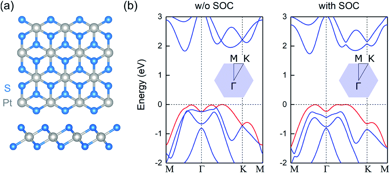 | ||
| Fig. 1 (a) Top and side views of the atomic structure of monolayer PtS2, where grey and blue spheres correspond to Pt and S atoms, respectively (b) electronic band structure of monolayer PtS2 without SOC (left panel) and with SOC (right panel). The energies refer to the VB maximum and the topmost VB is highlighted in red. The insets show the corresponding Brillouin zone. | ||
As observed in Fig. 1b, single-layer PtS2 is a semiconductor with an indirect band gap of Eg = 1.83 eV. The valence band (VB) maximum lies along the Γ–K direction, whereas the conduction band (CB) minimum is located between the Γ and M points, in agreement with previously reported theoretical calculations.21 The inclusion of spin–orbit coupling (SOC) reduces the gap by less than 0.1 eV, and retains the indirect nature of the gap. Interestingly, the topmost VB resembles an inverted Mexican-hat-like dispersion. This peculiar VB dispersion leads to a divergence in the density of states, corresponding to sharp van Hove singularities. When the Fermi level lies close to such singularities, the large electronic density of states favors the formation of a ferromagnetic order, since the Stoner criterion is satisfied.22–24 Thus, hole-doped 2D PtS2 can be a ferromagnetic material, similar to other 2D metal chalcogenides.6–8 Note that the inclusion of SOC preserves the sombrero shape VB and the subsequent van Hove singularity at the top of the VB and for the calculations of the magnetic and electronic properties of doped systems, this relativistic interaction is not included.
Initially, we consider charged supercells and we compute the magnetic moment and the spin polarization energy for different hole densities (n). The spin polarization energy is defined as the energy difference between the non-magnetic and the ferromagnetic phase, and positive values reveal a stable ferromagnetic phase. As observed in Fig. 2, at the low doping level, a ferromagnetic state spontaneously emerges and the magnetic moment reaches the saturation value of 1 μB per carrier. Although the magnetic moment per carrier remains constant up to high hole densities, the spin polarization energy per carrier significantly varies. In particular, for low hole densities, it increases by increasing the density, whereas for n = 3.5 × 10¹⁴/cm2, it reaches the maximum value of about 12 meV per carrier. Further increase of the hole density results in the reduction of the spin polarization energy.
 | ||
| Fig. 2 Magnetic moment and spin polarization energy as a function of the carrier density. | ||
It is worth noting that for charged slabs, the electrostatic potential significantly diverges with the distance from the slab, and the total energy strongly depends on the vacuum thickness. However, by increasing the vacuum thickness, even though the energy significantly varies, the energy difference between the non-magnetic and the ferromagnetic state remains unchanged.
Fig. 3 shows the spin-polarized density of states of charged supercells at various hole densities. At the low doping level, a slight splitting of the opposite spin-states near the Fermi level is observed. By increasing the hole density, the energy difference between the spin up and spin down VB maxima significantly increases, whereas the Fermi level is shifted to lower energies. This results in a half-metallic behavior where the majority and minority spin states exhibit insulating and metallic nature, respectively. Such behavior is highly promising for future spintronic applications, allowing a fully polarized spin transport in 2D PtS2.
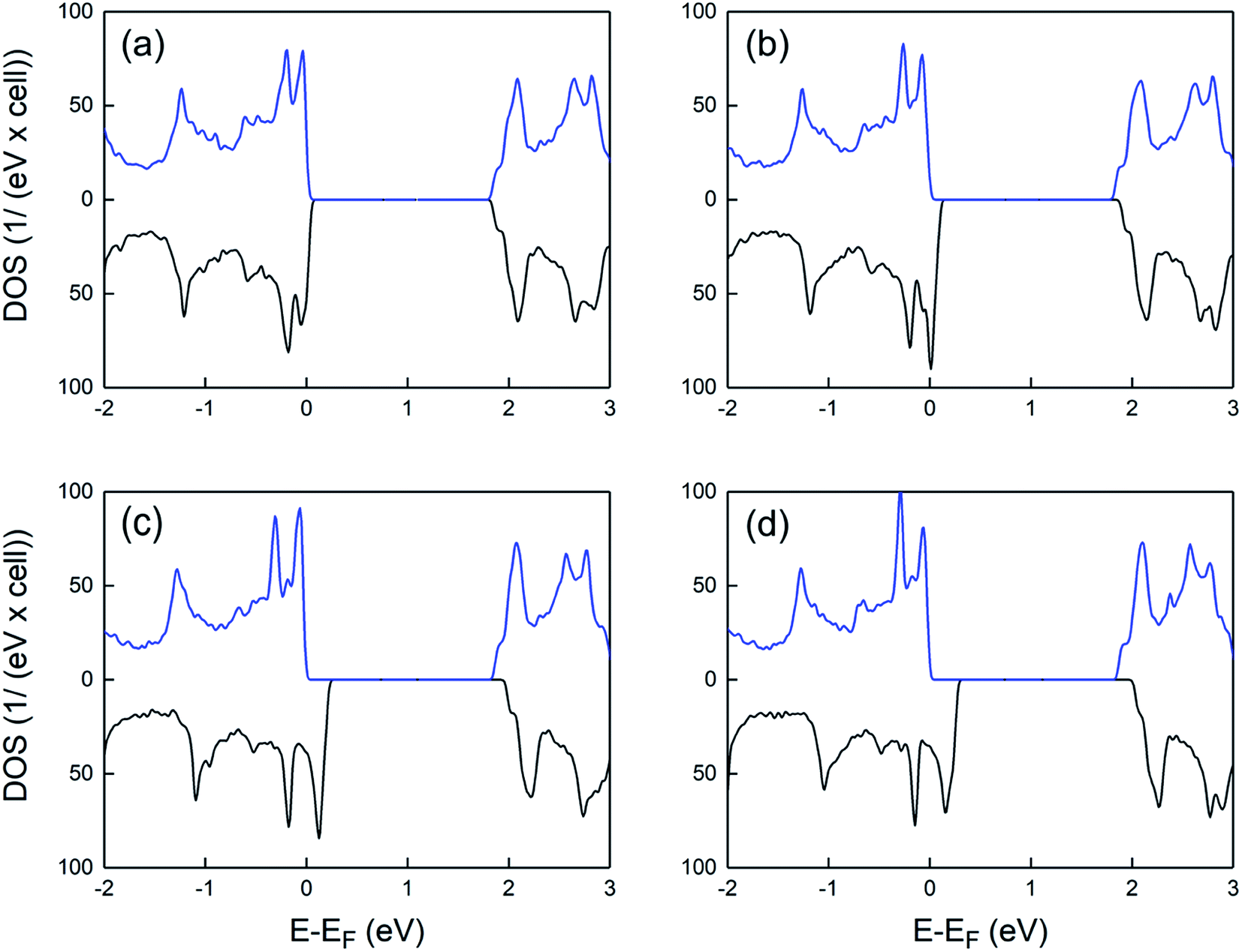 | ||
| Fig. 3 Density of states of charged supercells for different hole densities: (a) 0.6 × 10¹⁴/cm2 (b) 1.9 × 10¹⁴/cm2 (c) 3.8 × 10¹⁴/cm2 and (d) 4.4 × 10¹⁴/cm2. The spectra include a 0.02 eV Lorentzian broadening. Blue and black lines indicate spin-up-like and spin-down-like density of states, respectively. | ||
In order to verify that the conclusion for the hole doping induced ferromagnetism is not affected by the underestimation of the band gap within DFT, we additionally performed hybrid functional calculations. First, we computed the HSE band structure of pristine 2D PtS2 and we found a gap opening of about 0.8 eV. As a next step, the electronic and magnetic properties of hole-doped systems were computed. Similar to our PBE calculations, upon hole doping, a splitting of the opposite spin states near the Fermi level was observed (see ESI, Fig. S1†) and the magnetic moments were found to be 1 μB per carrier.
3.2 Hole doping induced by S substitution
Next, we consider 5 × 5 × 1 supercells and we study the substitution of S atoms by group-V atoms, namely X = N, P, and As. Taking into account that S atoms have six valence electrons whereas group-V atoms have only five electrons, such substitutional dopants are good candidates to induce hole doping and a subsequent ferromagnetic order in monolayer PtS2. Regarding the structural properties, Pt atoms neighboring the N and P atoms exhibit an inward relaxation of about 12.7 and 3.1%, resulting in shortened N–Pt and P–Pt bonds of 2.09 and 2.32 Å, respectively. By contrast, Pt atoms surrounding the rather large As anion relax outwards by about 1.9%, leading to elongated As–Pt bonds of 2.44 Å.To evaluate the thermodynamic stability of these dopants, we calculate the dopant formation energies using the equation
| Efor = Etot(PtS2:X) − Etot(PtS2) + μS − μX | (1) |
Next, the magnetic and electronic properties of doped systems are discussed. All substitutional dopants lead to magnetic ground states with total magnetic moments of 1 μB. The spin polarization energies are found to be 0.27, 0.10, and 0.06 eV, for N, P, and As, respectively, where the positive values reveal a stable (local) magnetic moment. The charge density differences as well as the spin density differences for all doped systems are shown in Fig. 4. The charge density difference is computed by Δρc = ρPtS2:X − ρPtS2:VS − ρX where ρPtS2:X, ρPtS2:VS, and ρX are the charge densities of doped PtS2 (i.e. PtS2 with a S substituent), bare PtS2:VS (i.e. PtS2 with a S vacancy), and isolated X dopants, respectively. Accordingly, the spin density difference, which is used to visualize the magnetic moment distribution around the dopant atom, is computed by Δρs = ρ↑ − ρ↓ where ρ↑ and ρ↓ are the spin up and spin down charge densities, respectively. To further describe the magnetic moment distribution, the ratio between the magnetic moment of the dopant atom and the total magnetic moment (Mr,X = MX/Mtot) is computed. We find Mr,N ≈ 66%, Mr,P ≈ 32%, and Mr,As ≈ 26%, i.e., the magnetic moment is less localized in the P and As doped systems, compared to the N doped one, as expected from the much deeper in-gap states for N doping.
 | ||
| Fig. 4 Charge density differences Δρc = ρPtS2:X − ρPtS2:VS − ρX (top panels) and spin density differences Δρs = ρ↑ − ρ↓ (bottom panels) of group-V doped systems. (a) and (d) N-on-S site, (b) and (e) P-on-S site, (c) and (f) As-on-S site. Purple, red and green spheres correspond to N, P, and As atoms, respectively. The isosurface value is 0.001 electrons per Å3. For the charge density differences, yellow and blue isosurfaces refer to electron accumulation and depletion, respectively. | ||
Regarding the electronic properties, as observed in Fig. 5, N creates two spin-polarized states within the gap. The occupied spin-up-like and unoccupied spin-down-like states are located ∼ 0.2 and 1.3 eV above the VB edge. Taking into account that the empty state lies far away from the VB, the substitution of S by N is unlikely to lead to a p-type behavior. Similar to N, both P and As dopants produce spin polarized states within the gap. By increasing the dopant atomic number, the gap states move towards the valence band and their spin splitting reduces. Note that the dependence of the spin splitting on the atomic number follows the trend for the exchange correlation integral.25,26 Overall, among all three dopants, As is the most promising one to induce p-type conductivity (provided a sufficient dopant concentration can be achieved), since the unoccupied gap state lies close to the VB edge. Our projected density of states calculations reveal that for all doped systems, the opposite spin states within the gap are mainly derived from the group-V p orbitals as well as the 5d orbitals of Pt atoms neighboring the group-V atom.
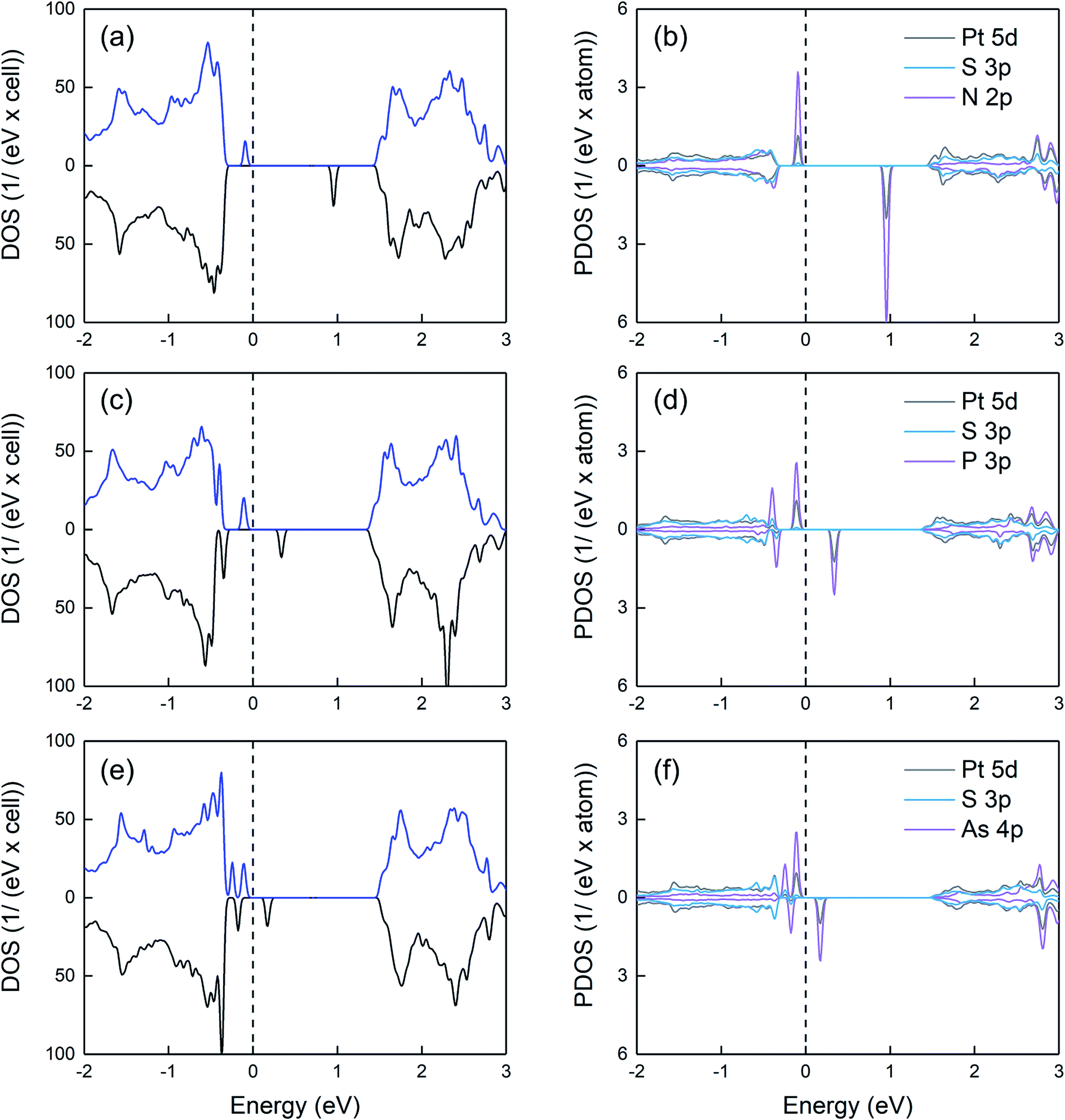 | ||
| Fig. 5 Density of states (left panels) and projected density of states (right panels) of group-V doped systems (a) and (b) N-on-S site, (c) and (d) P-on-S site, (e) and (f) As-on-S site. For the projected density of states, Pt and S neighboring the dopant atom are considered. The energies refer to the highest occupied state and the spectra include a 0.02 eV Lorentzian broadening. | ||
4. Conclusions
Based on first principles calculations, we studied the magnetic and electronic properties of hole-doped monolayer PtS2. Upon hole doping, a transition from a non-magnetic to a ferromagnetic phase along with a half-metallic behavior were observed. Therefore, hole-doped 2D PtS2 presenting one conducting and one insulating spin channel, could be highly promising for future spin-based nanodevices. Hole doping resulting from substitutional doping was also investigated. We found that group-V atoms replacing S atoms create spin polarized states within the gap. By increasing the dopant atomic number, these states move towards the valence band edge and their spin splitting reduces, potentially forming a ferromagnetic phase in monolayer PtS2.Conflicts of interest
There are no conflicts to declare.Acknowledgements
This work has been financially supported by the Research Council of Norway (ToppForsk project: 251131). We acknowledge access to HPC resources Abel and Fram in Norway with allocation provided through NOTUR.References
- X. Q. Lu, C. K. Wang and X. X. Fu, Modulating the electronic structures of blue phosphorene towards spintronics, Phys. Chem. Chem. Phys., 2019, 21, 11755 RSC.
- X. Li, X. Zuo, H. Li, L. Han, Q. Gao, D. Li, B. Cui, D. Liu and F. Qu, Exotic magnetism in As-doped α/β-In2Se3 monolayers with tunable anisotropic carrier mobility, Phys. Chem. Chem. Phys., 2019, 21, 19234 RSC.
- J. Tan, W. Li, X. He and M. Zhao, Stable ferromagnetism and half-metallicity in two-dimensional polyporphyrin frameworks, RSC Adv., 2013, 3, 7016 RSC.
- B. Huang, G. Clark, E. Navarro-Moratalla, D. R. Klein, R. Cheng, K. L. Seyler, D. Zhong, E. Schmidgall, M. A. McGuire, D. H. Cobden and W. Yao, Layer-dependent ferromagnetism in a van der Waals crystal down to the monolayer limit, Nature, 2017, 546, 270 CrossRef CAS PubMed.
- C. Gong, L. Lin, Z. Li, H. Ji, A. Stern, Y. Xia and T. Cao, et al., Discovery of intrinsic ferromagnetism in two-dimensional van der Waals crystals, Nature, 2017, 546, 265 CrossRef CAS PubMed.
- S. Wu, X. Dai, H. Yu, H. Fan, J. Hu and W. Yao, Magnetisms in p-Type Monolayer Gallium Chalcogenides (GaSe, GaS), arXiv: 1409.4733, 2014 Search PubMed.
- T. Cao, Z. Li and S. G. Louie, Tunable Magnetism and Half-Metallicity in Hole-Doped Monolayer GaSe, Phys. Rev. Lett., 2015, 114, 236602 CrossRef PubMed.
- K. Iordanidou, M. Houssa, J. Kioseoglou, V. V. Afanas’ ev, A. Stesmans and C. Persson, Hole-doped 2D InSe for spintronic applications, ACS Appl. Nano Mater., 2018, 1, 6656 CrossRef CAS.
- M. Houssa, R. Meng, K. Iordanidou, G. Pourtois, V. V. Afanas'ev and A. Stesmans, Stoner Ferromagnetism in Two-Dimensional Materials, ECS Trans., 2019, 92, 35–41 CrossRef.
- M. J. Piotrowski, R. K. Nomiyama and J. L. Da Silva, Role of van der Waals corrections for the PtX2 (X = O, S, Se) compounds, Phys. Rev. B, 2013, 88, 075421 CrossRef.
- F. A. Rasmussen and K. S. Thygesen, Computational 2D materials database: electronic structure of transition-metal dichalcogenides and oxides, J. Phys. Chem. C, 2015, 119, 13169 CrossRef CAS.
- W. Zhang, Z. Huang, W. Zhang and Y. Li, Two-dimensional semiconductors with possible high room temperature mobility, Nano Res., 2014, 7, 1731 CrossRef CAS.
- P. Manchanda, A. Enders, D. J. Sellmyer and R. Skomski, Hydrogen-induced ferromagnetism in two-dimensional Pt dichalcogenides, Phys. Rev. B, 2016, 94, 104426 CrossRef.
- G. Kresse and J. Furthmüller, Efficient Iterative Schemes for Ab Initio Total-Energy Calculations Using a Plane-Wave Basis Set, Phys. Rev. B, 1996, 54, 11169 CrossRef CAS PubMed.
- G. Kresse and J. Furthmüller, Efficiency of Ab-Initio Total Energy Calculations for Metals and Semiconductors Using a Plane-Wave Basis Set, Comput. Mater. Sci., 1996, 6, 15–50 CrossRef CAS.
- J. P. Perdew, K. Burke and M. Ernzerhof, Generalized Gradient Approximation Made Simple, Phys. Rev. Lett., 1996, 77, 3865 CrossRef CAS PubMed.
- S. Grimme, J. Antony, S. Ehrlich and S. Krieg, A Consistent and Accurate Ab Initio Parametrization of Density Functional Dispersion Correction (DFT-D) for the 94 Elements H-Pu, J. Chem. Phys., 2010, 132, 154104 CrossRef PubMed.
- P. E. Blöchl, Projector Augmented-Wave Method, Phys. Rev. B, 1994, 50, 17953 CrossRef PubMed.
- J. Heyd, G. E. Scuseria and M. Ernzerhof, Hybrid functionals based on a screened Coulomb potential, J. Chem. Phys., 2003, 118, 8207 CrossRef CAS.
- Y. Zhao, J. Qiao, P. Yu, Z. Hu, Z. Lin, S. P. Lau, Z. Liu, W. Ji and Y. Chai, Extraordinarily strong interlayer interaction in 2D layered PtS2, Adv. Mater., 2016, 28, 2399 CrossRef CAS PubMed.
- P. Miró, M. Ghorbani-Asl and T. Heine, “Two Dimensional Materials Beyond MoS2: Noble-Transition-Metal Dichalcogenides, Angew. Chem., Int. Ed., 2014, 53, 3015 CrossRef.
- L. Seixas, A. S. Rodin, A. Carvalho and A. C. Neto, Multiferroic Two-Dimensional Materials, Phys. Rev. Lett., 2016, 116, 206803 CrossRef CAS PubMed.
- M. Houssa, K. Iordanidou, G. Pourtois, V. V. Afanas' ev and A. Stesmans, Hole-Doping Induced Ferromagnetism in Monolayer SnO: A First-Principles Study, ECS Trans., 2017, 80, 339–345 CrossRef CAS.
- M. Houssa, K. Iordanidou, G. Pourtois, V. V. Afanas’ev and A. Stesmans, Ferromagnetism in Two-Dimensional Hole-Doped SnO, AIP Adv., 2018, 8, 055010 CrossRef.
- J. F. Janak, Uniform Susceptibilities of Metallic Elements, Phys. Rev. B, 1977, 16, 255 CrossRef CAS.
- K. Dolui, I. Rungger, C. D. Pemmaraju and S. Sanvito, Possible Doping Strategies for MoS2 Monolayers: An Ab Initio Study, Phys. Rev. B, 2013, 88, 075420 CrossRef.
Footnote |
| † Electronic supplementary information (ESI) available. See DOI: 10.1039/c9ra09756b |
| This journal is © The Royal Society of Chemistry 2020 |