
 Open Access Article
 This Open Access Article is licensed under a Creative Commons Attribution-Non Commercial 3.0 Unported Licence
A hillock-like phenomenon with low friction and adhesion on a graphene surface induced by relative sliding at the interface of graphene and the SiO2 substrate using an AFM tip
Na
Fan†
 a,
Jian
Guo†
ab,
Guangyin
Jing
c,
Cheng
Liu
a,
Qun
Wang
a,
Guiyong
Wu
a,
Hai
Jiang
a and
Bei
Peng
*a
a,
Jian
Guo†
ab,
Guangyin
Jing
c,
Cheng
Liu
a,
Qun
Wang
a,
Guiyong
Wu
a,
Hai
Jiang
a and
Bei
Peng
*a
aSchool of Mechanical and Electrical Engineering, University of Electronic Science and Technology of China, Chengdu 611731, China. E-mail: beipeng@uestc.edu.cn
bSchool of Mechanical Engineering, University of South China, Hengyang 421001, China
cNational Key Laboratory and Incubation Base of Photoelectric Technology and Functional Materials, School of Physics, Northwest University, Xi'an 710069, China
First published on 10th April 2020
Abstract
Graphene demonstrates high potential as an atomically thin solid lubricant for sliding interfaces in industry. However, graphene as a coating material does not always exhibit strong adhesion to any substrates. When the adhesion of graphene to its substrate weakens, it remains unknown whether relative sliding at the interface exists and how the tribological properties of the graphene coating changes. In this work, we first designed a method to weaken the adhesion between graphene and its SiO2 substrate. Then the graphene with weakened adhesion to its substrate was rubbed using an AFM tip, where we found a novel phenomenon: the monolayer graphene not only no longer protected the SiO2 substrate from deformation and damage, but also prompted the formation of hillock-like structures with heights of approximately tens of nanometers. Moreover, the surface of the hillock-like structure exhibited very low adhesion and a continuously decreasing friction force versus sliding time. Comparing the hillock-like structure on the bare SiO2 surface and the proposed force model, we demonstrated that the emergence of the hillock-like structure (with very low adhesion and continuously decreasing friction) was ascribed to the relative sliding at the graphene/substrate interface caused by the mechanical shear of the AFM tip. Our findings reveal a potential failure of the graphene coating when the adhesion strength between graphene and its substrate is damaged or weakened and provide a possibility for in situ fabrication of a low friction and adhesion micro/nanostructure on a SiO2/graphene surface.
Introduction
Recently, two-dimensional (2D) materials have attracted significant interest due to their ability to reduce friction further due to the weak interlayer van der Waals interaction.1–3 Accordingly, atomically thin graphene indicates promising prospects for the lubrication of micro/nano-electromechanical systems (MEMS/NEMS) because of its excellent tribological properties;4–8 hence, the nanotribological study of graphene has gradually become a popular research topic relating to 2D materials. Many experimental studies have revealed the unique nanotribological properties of graphene, namely, the friction force of graphene decreasing with the increasing numbers of layers.4,9 Some researchers have also reported results regarding superlubricity and ultralow friction of graphene,10–14 such as superlubric sliding of graphene nanoscrolls on diamond like carbon11 and superlubric sliding of graphene-coated microspheres on graphene.12The adhesion between graphene and its substrate has been found to play an important role in the nanotribological behaviour of graphene. Zeng et al.15,16 indicated that the friction force on the graphene surface could be controlled by changing the adhesion strength between graphene and its substrate by plasma treatment of the substrate. In addition, it was found that different substrates (such as Ni, SiO2, and PDMS) have different influences on the friction force of graphene, due to significantly different adhesion energies at the graphene/substrate interfaces.17,18 Conversely, the direct measurement method of adhesion properties between graphene and different substrates involving silicon and metal substrates was successively proposed.19–21 In most cases, graphene cannot be directly grown on the desired substrates but first needs to be grown on another substrate and then physically transferred onto the target substrate.22,23 Because the adhesion strength between graphene and the target substrate depends highly on the transfer process, the nanotribological properties of graphene may be compromised by this physical transfer process. However, tribological studies have been conducted recently in which graphene adheres well to its substrate. Given that graphene does not always have strong adhesion to many substrates, the tribological properties of graphene in the case of weakened adhesion are unclear.
It has been reported that the adhesion of graphene to the SiO2 substrate is weaker than that to metal substrates;17 therefore, it is easier to weaken the adhesion between graphene and the SiO2 substrate. In this study, we first designed an experiment to reduce the adhesion strength at the interface of graphene and its SiO2 substrate. Then, we found that graphene would not protect its SiO2 substrate well due to producing the so-called friction-induced hillock,24,25 but prompt the formation of a higher hillock-like structure on the SiO2/graphene surface. Moreover, we conducted comparative analysis between the friction and adhesion forces for four different surfaces, as follows: a bare SiO2 substrate, graphene covered on the SiO2 substrate, graphene suspended on the grooves, and a SiO2/graphene hillock-like structure. The results indicated that the surface of the hillock-like structure exhibited very low adhesion and continuously decreasing friction versus sliding time. Comparing the hillock-like structure on bare SiO2 and the proposed force model, we demonstrated that the emergence of the hillock-like structure (with very low adhesion and continuously decreasing friction) was related to the relative sliding at the interface of graphene and the SiO2 substrate.
Previous studies have found that the environmental sensitivity,26,27 edge effect,28 and defects29,30 of graphene can cause the failure of the graphene coating. Our work revealed another potential failure of graphene: when the adhesion strength between graphene and its substrate is weakened (or even broken), a relative sliding at the interface of graphene/substrate occurs, along with the formation of a hillock-like structure on the SiO2/graphene surface. Conversely, our work could offer the possibility of in situ fabrication of the micro/nanostructure with low friction and adhesion on the SiO2/graphene surface, which may have potential applications in micro- and nano-devices, such as miniature gear and micro turbines or any other friction pairs on the micro- and nano-scale.
Results and discussion
(I) Hillock-like phenomena on the SiO2/graphene surface
To study the nanotribological properties of graphene when the adhesion strength between graphene and the SiO2 substrate was weakened, we designed and performed a corresponding experiment, as shown in Fig. 1. Fig. 1a shows that the monolayer graphene was successfully transferred on the SiO2 substrate patterned with a groove-array structure. It can be noted that parts of the graphene were suspended on the grooves (namely suspended graphene) and the other parts adhered well to the SiO2 substrate surface (namely supported graphene). AFM experiments were conducted on both the suspended graphene region and supported graphene region. Fig. 1b–d show in detail the generation procedure of the hillock-like structure: (i) first, the suspended graphene was rubbed using an AFM Si tip under a certain normal load (Fig. 1b). As a result, the adhesion strength between the graphene and SiO2 substrate is gradually weakened by the mechanical shear of the AFM tip. (ii) Second, the suspended graphene slides along the SiO2 substrate, resulting in more graphene sinking into the groove where the tip rubs, where the adhesion strength between the graphene and SiO2 substrate changes from strong to weak (Fig. 1c). (iii) Finally, the AFM tip rubs the supported graphene region (Fig. 1d), testing the tribological behaviour of the new SiO2/graphene surface with weak adhesion at the interface of the supported graphene and SiO2 substrate. Raman spectral analysis results indicated that the graphene sample was monolayer graphene, determined from the intensity ratios of 2D and G peaks, as shown in Fig. 1e.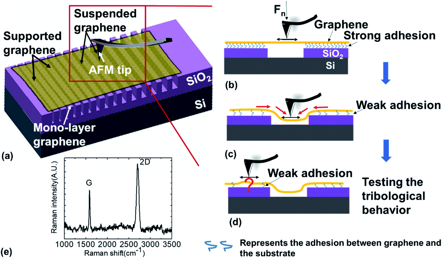 | ||
| Fig. 1 Schematic diagram showing the experimental process. (a) Schematic structure of the monolayer graphene transferred onto the groove-patterned SiO2 substrate surface, where some of the graphene is suspended in the grooves and some adheres to the pattern-less SiO2 substrate surface. (b–d) Schematic drawing of the experimental design with the interactions the between silicon tip and suspended monolayer graphene. First, a friction experiment is performed on the suspended graphene surface using an AFM Si tip; as a result, the adhesion strength would be gradually weakened by mechanical shear action. Second, the suspended graphene slides along the groove and sinks (to some extent) into the groove. Finally, the silicon tip rubbed the supported graphene region and tested the tribological behaviour of the new SiO2/graphene surface. (e) Typical Raman spectra with the intensity ratios of 2D and G peaks demonstrating that the sample is monolayer graphene films. | ||
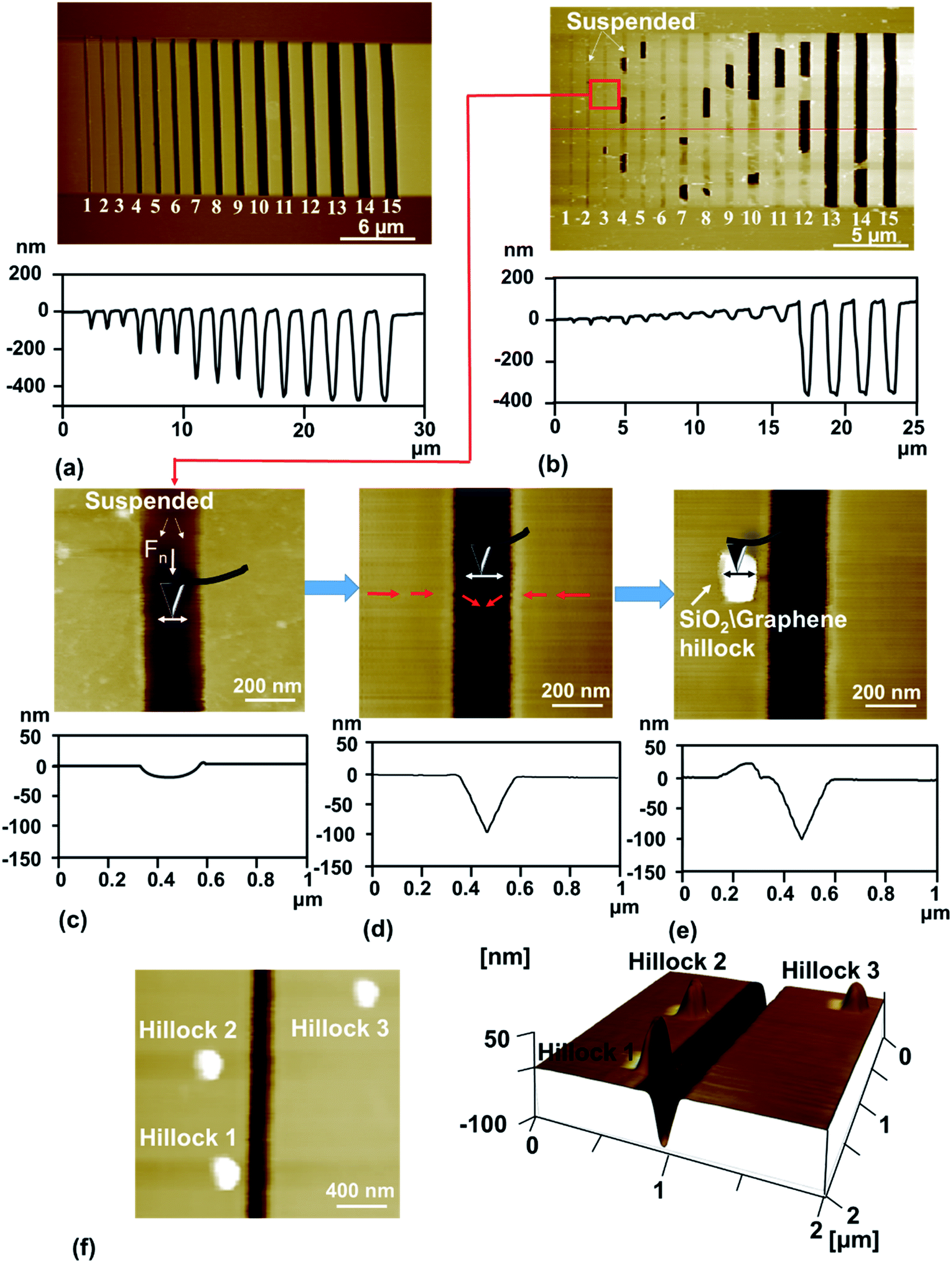 | ||
| Fig. 2 Formation process of the hillock-like structure on the supported graphene surface. (a) AFM image (top) and cross-sectional profile (bottom) of the groove-patterned SiO2 substrate. (b) AFM image (top) and cross-sectional profile along the red line (bottom) of monolayer graphene transferred onto the groove-patterned SiO2 substrate. (c) AFM image and the cross-sectional profile showing the in situ region before silicon tip rubbing of the suspended graphene. (d) AFM image and cross-sectional profile showing the in situ region after silicon tip rubbing of the suspended monolayer graphene. (e) AFM image and the cross-sectional profile showing the in situ region after tip rubbing of the supported graphene surface near the groove, where a hillock-like structure with a height of ∼20 nm is observed. (f) 2D topography (left) and 3D topography (right) of three hillock-like structures produced on the sliding surface of the suspended monolayer graphene. | ||
To investigate the stability and evolution of the hillock-like structure on the SiO2/graphene surface further, we conducted scratching and indentation experiments with the AFM Si tips. First, scratching experiments were carried out on the surface of the hillock structure under a normal load Fn of 150 nN and sliding cycles (N = 10) over a sliding area of 50 × 50 nm. As illustrated in Fig. 3, the height of the hillock-like structure increased from ∼20 nm (Fig. 3a) to ∼60 nm (Fig. 3b) after scratching. After continuing to scratch the hillock-like structure in the same way, the height of the hillock-like structure decreased from ∼60 nm (Fig. 3b) to ∼45 nm (Fig. 3c). Subsequently, an indentation experiment was performed on the hillock-like structure surface under a normal load Fn of 1 μN and different numbers of indentation cycles of 10, 50 and 100, as shown in Fig. 4. Fig. 4a presents a hillock-like structure with a height of ∼20 nm, produced under a normal load Fn of 150 nN and sliding cycles (N = 10). It was observed that after 50 indentations, a 1 nm deep pit was generated on the surface of the hillock-like structure (Fig. 4c). A deeper pit formed when the number of the indentation cycles was increased to 100 (Fig. 4d). By contrast, when the same indentation and scratching tests were performed on the original SiO2/graphene surface with good adhesion, the pit and the hillock-like structure could not form in the indentation and scratching region, which suggests that the mechanical properties of the hillock-like structure were notably different from those of the original SiO2/graphene. Because the hardness of graphene is much higher than that of the AFM Si tip, we considered that the hillock-like structure was related to the thick SiO2 substrate rather than the deformation of graphene.
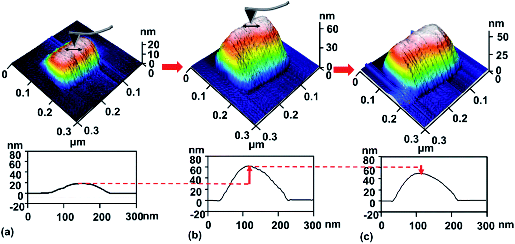 | ||
| Fig. 3 Scratching tests on the hillock-like structure surface. (a) A hillock-like structure with a height of ∼20 nm on the supported graphene surface; (b) and (c), respectively, show that after the scratching test, the height of the hillock-like structure increased from ∼20 nm to ∼60 nm, and then decreased from ∼60 nm to ∼45 nm. | ||
 | ||
| Fig. 4 Indentation tests with different numbers of indenting cycles on the hillock-like structure surface. (a) A hillock-like structure on the supported monolayer graphene surface before the indentation tests; (b), (c), and (d) show the topography variation of the hillock-like structure with the number of indentation cycles of 10, 50, and 100 times, respectively. The applied normal load Fn during such tests was 1 μN. The scale bars in the AFM images were 50 nm. | ||
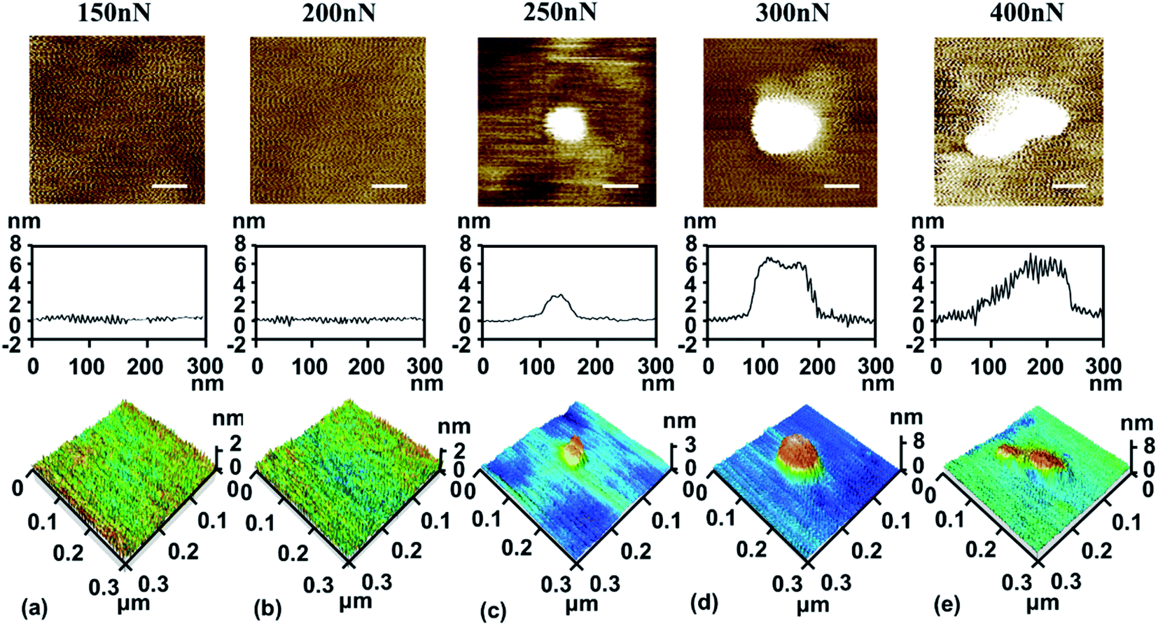 | ||
| Fig. 5 Effect of normal load on the friction-induced hillock structure on the bare SiO2 surface. The sliding tests are performed on five regions with an area of 100 nm × 100 nm under the normal loads of 150 nN, 200 nN, 250 nN, 300 nN and 400 nN, respectively. The scale bars in this figure are 60 nm. | ||
By comparing Fig. 2 and 5, the difference between the hillock-like structure on the SiO2/graphene surface and the hillock structure on the bare SiO2 surface can be clearly seen. We speculated that after AFM tip rubbing, the suspended graphene under a given normal load and number of sliding cycles, would demonstrate a weakened adhesion strength between graphene and its SiO2 substrate, and relative movement would occur at this interface. Thus, when the AFM tip rubbed the supported graphene, the SiO2 substrate was not only rubbed by the tip but the tip and the attached graphene worked together. In other words, the tip and the attached graphene—with some warping—constituted a new ‘tip’ to rub the SiO2 substrate; because of the stronger mechanical interaction induced by this ‘tip’ in comparison to the Si tip only, the hillock-like structure would be more easily produced.
Here, we summarised the different states of the bare SiO2 surface, strong-adhesion SiO2/graphene surface, and weak-adhesion SiO2/graphene surface when rubbed using the Si tip, as shown in Fig. 6. Fig. 6a shows that a friction-induced hillock structure could be directly produced on the SiO2 surface after Si tip rubbing, suggesting that some deformation or lattice change has taken place in SiO2 crystals, which was also discovered in previous studies.24,25 In the case of strong adhesion between graphene and its SiO2 substrate, graphene as a coating can protect the SiO2 substrate well against the mechanical shear of the Si tip, thus preventing the formation of the hillock-like structure, as shown in Fig. 6b. In fact, it is difficult to guarantee that the graphene always adheres well with its substrate in such an application scenario. To understand what would happen if the tip rubbed the graphene adhered weakly with its substrate, we designed an experiment as shown in Fig. 6c. First, we rubbed the suspended graphene with an AFM tip and made the suspended graphene sink into the groove. As a result, the adhesion strength between graphene and the SiO2 substrate was weakened, causing the graphene supported on the substrate to move with the substrate. The initial time when the adhesion of graphene to the substrate became weak is denoted as time t0. As the tip rubs against the graphene surface, the graphene slides relative to the SiO2 substrate, denoted as time t1. With the continuous rubbing of the AFM tip, the adhesion of graphene to the substrate becomes weaker and weaker, denoted as time t2, at which graphene directly interacts with the substrate during the movement of the tip. Finally, a hillock-like structure with a height of approximately tens of nanometers forms in situ on the sliding monolayer graphene. The SiO2/graphene hillock-like structure may be formed from the deformed SiO2 or combined with the puckering graphene as mentioned in the previous study31–33 and the deformed SiO2.
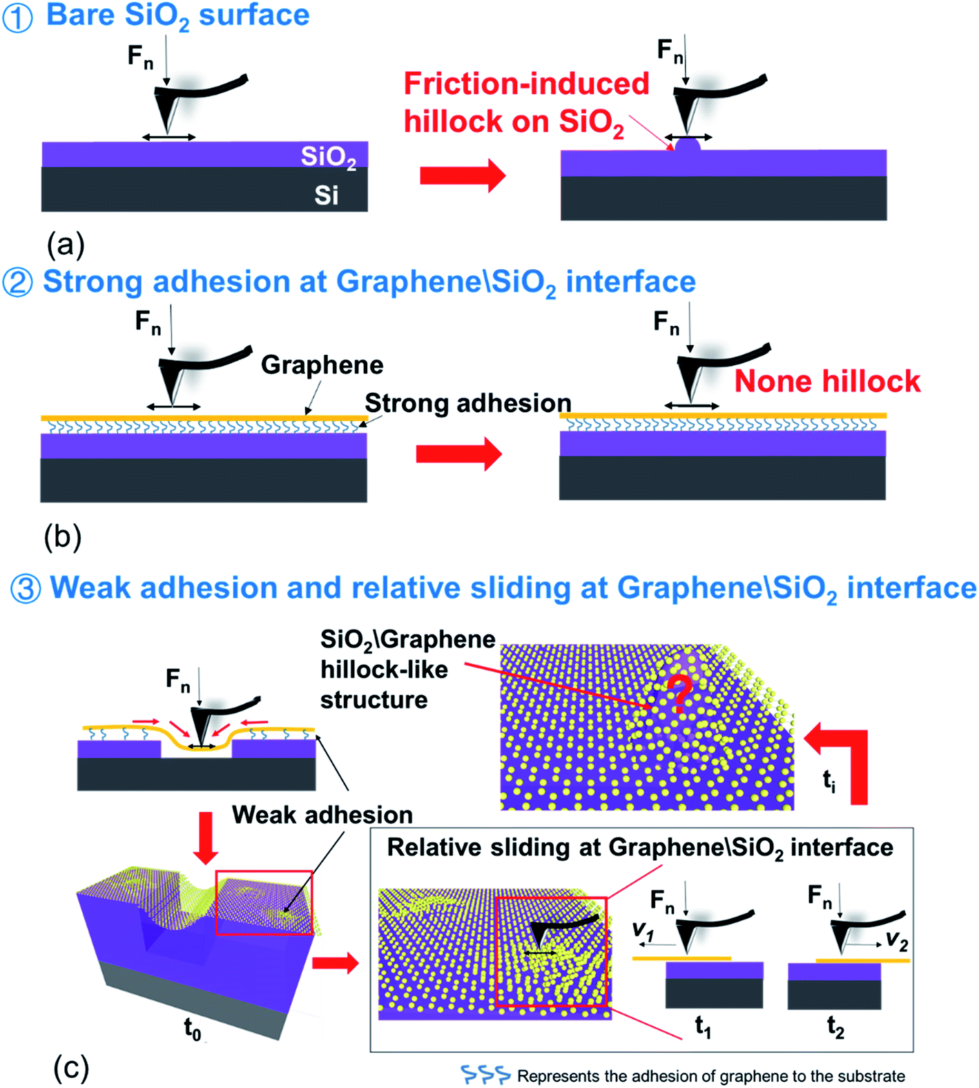 | ||
| Fig. 6 Three different situations of the friction behaviour when rubbed using the AFM tip. (a) Bare SiO2 surface rubbed with the AFM tip and a corresponding friction-induced hillock appearing on the SiO2 surface. (b) No hillock-like structure occurs when a graphene coating covers the SiO2 surface where the graphene adheres well on its substrate. (c) A relative sliding at the interface of the graphene and SiO2 substrate would occur when the adhesion at the interface is weakened, which results in a SiO2/graphene hillock-like structure. | ||
Compared with these three different situations described, a hypothesis has been proposed that when the adhesion of graphene to its substrate weakened, it could result in the relative sliding occurring at the interface of graphene and the substrate. In order to prove the hypothesis and demonstrate the SiO2/graphene hillock-like structure, we conducted friction force and adhesion force tests as follows.
(II) A relative sliding at the interface of the graphene and SiO2 substrate
In order to prove the hypothesis that the relative sliding would occur at the interface of graphene and the substrate when the adhesion of graphene to its substrate is weakened, we measured the friction force (Fig. 7) on four different surfaces, namely the SiO2 surface, supported graphene surface, suspended graphene surface, and hillock-like structure surface. Fig. 7a and b show the variation of friction force as a function of the sliding time on the four different surfaces, where the friction force value was obtained in the area-scan mode with an area of 100 × 100 nm using AFM, under the normal loads of 5 and 10 nN. It was found that the average friction force values on the four different surfaces had the following relationship: the SiO2 substrate > the supported graphene > the suspended graphene > the hillock-like structure. In addition, it is notable that the friction force on the hillock-like structure surface demonstrated a significantly different situation compared to that on the other three surfaces: the friction force gradually decreased with the sliding time, while the friction forces on the other three surfaces remained stable. Because the normal load is too low to cause the wear or deformation of graphene, the almost unchanged friction force versus sliding time on supported graphene and suspended graphene surfaces could be well understood. | ||
| Fig. 7 Measurement of friction force on the SiO2 substrate, supported graphene, suspended graphene and the hillock-like structure on the SiO2/graphene surface under the normal loads of 5 nN (a) and 10 nN (b). | ||
We speculated that such a situation for the hillock-like structure was related to the result of the relative sliding at the interface of the SiO2 substrate and graphene due to the movement of the AFM tip. Fig. 8 shows the model of the friction structure when relative sliding occurred at the interface of graphene and the substrate; from top to bottom: AFM tip (A), graphene (B), and SiO2 substrate (C). When the AFM tip moves in a certain direction with a velocity v, the force analysis of A, B, and C in the lateral direction is as presented in this figure. To analyse the resultant force of graphene, the following relationships should be satisfied:
| FB = FAB + FCB = mBαB | (1) |
| FAB = FCB | (2) |
 | ||
| Fig. 8 Schematic diagram showing the friction behavior of the AFM tip/graphene/SiO2 substrate when a relative sliding occurs at the interface of graphene and the SiO2 substrate. | ||
Thus, it is suggested that the tangential force on the hillock-like structure surface (the curve with the green colour in Fig. 7) equalled the tangential force of graphene on the SiO2 substrate. The initial friction force value of the hillock-like structure surface is the lowest compared to other cases as shown in Fig. 7, which is in agreement with the experimental results reported by Liu et al.12 This study reveals that the friction force of the graphene-coated SiO2 tip (that is, graphene grown directly on the SiO2 microsphere surface) against the SiO2 substrate is much lower than that of the SiO2 tip against the graphene substrate. Our experiment showed that the friction force of the hillock-like structure surface was lower than that of the suspended graphene, which could prove the existence of the relative sliding occurring at the interface of the graphene and SiO2 substrate. During the continuous rubbing process with the AFM tip, the adhesion strength between graphene and the substrate was gradually weakened along with the relative motion of graphene and the substrate, resulting in the continued decrease in the friction resistance of graphene. This phenomenon was reflected in the experiment, that is, the measured friction force value gradually decreased versus sliding time (show in Fig. 7).
(III) Formation of the hillock-like structure by deformed SiO2
In order to illustrate what the SiO2/graphene hillock-like structure is, deformed SiO2 or a combination of puckering graphene and the deformed SiO2, we conduct the adhesion force test. Fig. 9a and b show the difference of adhesion force on the four different surfaces, which indicates that (i) the adhesion force on the SiO2 surface (∼108 nN) was much higher than those on the other three surfaces; (ii) the adhesion force on the supported graphene surface and the suspended graphene (without the substrate effect) was similar (∼50 nN), indicating that the SiO2 substrate had a little influence on the adhesion force in our experiment; and (iii) it is notable that the hillock-like structure surface showed the lowest adhesion force (∼10 nN). | ||
| Fig. 9 (a) Adhesion force map covering the SiO2 substrate, the supported graphene, the suspended graphene, and the hillock-like structure on the SiO2/graphene surface. (b) Statistics of the adhesion force on the above four surfaces. | ||
It is well known that the adhesion force is mainly the van der Waals force, consisting of the Keesom, Debye, and London dispersion forces34 where the London dispersion force (as a result of two instantaneously induced dipoles acting on each other) plays a dominant role. The previous results have already shown that when graphene and its SiO2 substrate adhered well with no relative sliding occurring on their interface, the distribution of graphene dipoles did not change, compared to the suspended graphene without the substrate. Hence, the supported graphene surface and the suspended graphene exhibited a similar value of adhesion force, as already shown in Fig. 9. Nevertheless, the significant decrease in the adhesion force of the hillock-like structure surface was related to the change in the distribution of graphene dipoles induced by the friction at these interfaces. In fact, SiO2 is a polarisable material and the electrostatic interaction between graphene and the SiO2 substrate has been described.35 By analysing the electrostatic interactions between monolayer graphene and a SiO2 substrate, Sabio et al.36 found that the polar modes on the SiO2 surface and the water molecules between graphene and SiO2 were the main factors affecting the electrostatic interaction between graphene and substrate. Given that our experiments were conducted in an air environment, after relative sliding at the graphene/SiO2 interface induced by the AFM tip, either polar modes of SiO2 or water molecules in the air directly affected the distribution of graphene dipoles during the friction process, as shown in Fig. 10. Therefore, the much lower adhesion of the hillock-like structure not only suggested that a relative movement had occurred between graphene and the SiO2 substrate in our experiment, but also proved that the SiO2/graphene hillock-like structure was generated by the deformation of the SiO2 substrate since the electrostatic interaction can only occur between graphene and SiO2. If there is puckering graphene, the adhesion force of the hillock-like structure should be the same as that of the suspended graphene.
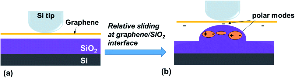 | ||
| Fig. 10 Interaction with polar modes at the interface of graphene and the SiO2 substrate before (a) and after (b) the relative sliding occurring at the interface. | ||
Conclusions
With its ultra-high strength and bearing capacity, graphene can form a continuous transfer film with self-lubrication and high bonding properties by combining with other materials, which is beneficial for reducing the friction coefficient and improving wear resistance. However, graphene does not always adhere well to many substrates, and the adhesion strength of graphene to its substrate can be easily weakened during the friction process, even resulting in ultimate failure. Nevertheless, the vast majority of experiments on graphene coating are carried out in the case of the strong adhesion of graphene to the substrate, rather than with a weak adhesion of graphene to the substrate.In this study, the main purpose was to examine the tribological properties of the graphene surface when the adhesion of graphene to the SiO2 substrate was weakened, as well as the interaction between graphene and its substrate. First, we designed an experiment to weaken the adhesion between graphene and the SiO2 substrate. Second, the graphene with a weakened adhesion to its substrate was rubbed with an AFM tip and it was found that the monolayer graphene as a coating lost its protective effect on the SiO2 substrate, such that the structure was deformed, even damaged, in the SiO2 substrate. The AFM tip and the covered graphene with weak adhesion to SiO2 substrate together rubbed the SiO2 substrate, prompting the formation of a higher hillock-like structure with a height of approximately tens of nanometers on the SiO2/graphene surface. Moreover, we found that tribological properties such as friction and adhesion forces of SiO2/graphene hillock-like structures were significantly different from those of the original SiO2/graphene surface, that is, the hillock-like structure exhibited very a low adhesion and a continuously decreasing friction force versus sliding time. Compared with the hillock-like structure on the bare SiO2 surface as well as combined with the proposed force model, we demonstrated that with the emergence of the hillock-like structure, very low adhesion and continuously decreasing friction was induced by the relative sliding at the graphene/substrate interface by the movement of the AFM tip.
To sum up, this work revealed the possibility of the occurrence of relative sliding at the interface of graphene and the SiO2 substrate when graphene weakly adheres to its substrate, along with a formation of a hillock-like structure on the SiO2/graphene surface. This finding suggests a potential failure of the graphene coating when the adhesion strength between graphene and its substrate is weakened. Conversely, it provides a possibility for in situ fabrication of the low friction and adhesion hillock structure on the SiO2/graphene surface that could be applied in micro- and nano-devices.
Experimental section
Growth of monolayer graphene using the CVD technique
The monolayer graphene film was grown using the chemical vapour deposition (CVD) method on a 25 μm thick 99.8% copper foil.37 We placed the copper foil in a CVD furnace and heated it to 985 °C for 20 min with CH4 (35 sccm) and H2 (2 sccm) as the sources, in a vacuum of 500 mTorr. After the growth, the sample was cooled until the temperature decreased to less than 100 °C. We confirmed by Raman spectroscopy that the monolayer graphene film was grown on the Cu foil.Conflicts of interest
The authors declare no conflict of interest.Acknowledgements
The authors would like to acknowledge the financial support from the Natural Science Foundation of China (51805240 and 51975107), the Project of International Science and Technology Cooperation and Exchange of Sichuan (2019YFH0017), and the Fundamental Research Funds for the Central Universities (No. ZYGX2019J037). We want to thank Prof. Chun Li for his support on the fabrication of the patterned Si/SiO2 substrates and Prof. Qiye Wen for his help with graphene transfer.References
- J. S. Choi, J. S. Kim, I. S. Byun, D. H. Lee, M. J. Lee, B. H. Park, C. Lee, D. Yoon, H. Cheong, K. H. Lee, Y. W. Son, J. Y. Park and M. Salmeron, Science, 2011, 333, 607–610 CrossRef CAS PubMed.
- H. Xiao and S. Liu, Mater. Des., 2017, 135, 319–332 CrossRef CAS.
- L. Liu, M. Zhou, X. Li, L. Jin, G. Su, Y. Mo, L. Li, H. Zhu and Y. Tian, Materials, 2018, 11, 1314 CrossRef PubMed.
- C. Lee, Q. Li, W. Kalb, X. Z. Liu, H. Berger, R. W. Carpick and J. Hone, Science, 2010, 328, 79–80 Search PubMed.
- K. S. Kim, H. J. Lee, C. Lee, S. K. Lee, H. Jang, J. H. Ahn, J. H. Kim and H. J. Lee, ACS Nano, 2011, 5, 5107–5144 CrossRef CAS PubMed.
- D. Berman, A. Erdemir and A. V. Sumant, Mater. Today, 2014, 17, 31–42 CrossRef CAS.
- Y. T. Peng, Z. Q. Wang and K. Zou, Langmuir, 2015, 31, 7782–7791 CrossRef CAS PubMed.
- X. Y. Ge, J. J. Li, H. D. Wang, C. H. Zhang, Y. H. Liu and J. B. Luo, Carbon, 2019, 151, 76–83 CrossRef CAS.
- Z. Deng, N. N. Klimov, S. D. Solares, T. Li, H. Xu and R. J. Cannara, Langmuir, 2013, 29, 235–243 CrossRef CAS PubMed.
- H. Deng, M. Ma, Y. M. Song, Q. C. He and Q. S. Zheng, Nanoscale, 2017, 1–6 Search PubMed.
- D. Berman, S. A. Deshmukh, S. K. R. S. Sankaranarayanan, A. Erdemir and A. V. Sumant, Science, 2015, 348, 1118–1122 CrossRef CAS PubMed.
- S. W. Liu, H. P. Wang, Q. Xu, T. B. Ma, G. Yu, C. H. Zhang, D. C. Geng, Z. W. Yu, S. G. Zhang, W. Z. Wang, Y. Z. Hu, H. Wang and J. B. Luo, Nat. Commun., 2017, 8, 14029 CrossRef CAS PubMed.
- X. H. Zheng, L. Gao, Q. Z. Yao, Q. Y. Li, M. Zhang, X. M. Xie, S. Qiao, G. Wang, T. B. Ma, Z. F. Di, J. B. Luo and X. Wang, Nat. Commun., 2016, 7, 13204 CrossRef CAS PubMed.
- Y. M. Liu, A. S. Song, Z. Xu, R. L. Zong, J. Zhang, W. Y. Yang, R. Wang, Y. Z. Hu, J. B. Luo and T. B. Ma, ACS Nano, 2018, 12, 7638–7646 CrossRef CAS PubMed.
- X. Z. Zeng, Y. T. Peng and H. J. Lang, Carbon, 2017, 118, 233–240 CrossRef CAS.
- X. Z. Zeng, Y. T. Peng, H. J. Lang and L. Liu, Sci. Rep., 2017, 7, 41891 CrossRef CAS PubMed.
- J. Torres, Y. Zhu, P. Liu, S. C. Lim and M. Yun, Phys. Status Solidi, 2018, 215, 1700512 CrossRef.
- Y. T. Peng, X. Z. Zeng, L. Liu, X. G. Cao, K. Zou and R. Chen, Carbon, 2017, 124, 541–546 CrossRef CAS.
- Z. Zong, C. L. Chen, M. R. Dokmeci and K. T. Wan, J. Appl. Phys., 2010, 107, 026104 CrossRef.
- G. Paolicelli, M. Tripathi, V. Corradini, A. Candini and S. Valeri, Nanotechnology, 2015, 26, 055703 CrossRef CAS PubMed.
- J. S. Bunch and M. L. Dunn, Solid State Commun., 2012, 152, 1359–1364 CrossRef CAS.
- A. C. Ferrari, F. Bonaccorso, V. Fal’ko, K. S. Novoselov, S. Roche, P. Bøggild, S. Borini, F. H. L. Koppens, V. Palermo, N. Pugno, J. A. Garrido, R. Sordan, A. Bianco, L. Ballerini, M. Prato, E. Lidorikis, J. Kivioja, C. Marinelli, T. Ryhänen, A. Morpurgo, J. N. Coleman, V. Nicolosi, L. Colombo, A. Fert, M. Garcia-Hernandez, A. Bachtold, G. F. Schneider, F. Guinea, C. Dekker, M. Barbone, Z. Sun, C. Galiotis, A. N. Grigorenko, G. Konstantatos, A. Kis, M. Katsnelson, L. Vandersypen, A. Loiseau, V. Morandi, D. Neumaier, E. Treossi, V. Pellegrini, M. Polini, A. Tredicucci, G. M. Williams, B. Hee Hong, J.-H. Ahn, J. Min Kim, H. Zirath, B. J. van Wees, H. van der Zant, L. Occhipinti, A. Di Matteo, I. A. Kinloch, T. Seyller, E. Quesnel, X. Feng, K. Teo, N. Rupesinghe, P. Hakonen, S. R. T. Neil, Q. Tannock, T. Löfwander and J. Kinaret, Nanoscale, 2015, 7, 4598–4810 RSC.
- S. Das, D. Lahiri, D. Y. Lee, A. Agarwal and W. Choi, Carbon, 2013, 59, 121–129 CrossRef CAS.
- C. F. Song, X. Y. Li, B. J. Yu, H. S. Dong, L. M. Qian and Z. R. Zhou, Nanoscale Res. Lett., 2011, 6, 310 CrossRef PubMed.
- B. J. Yu, H. S. Dong, L. M. Qian, Y. F. Chen, J. X. Yu and Z. R. Zhou, Nanotechnology, 2009, 20, 465303 CrossRef PubMed.
- P. Gong, Z. J. Ye, L. Yuan and P. Egberts, Carbon, 2018, 132, 749–759 CrossRef CAS.
- H. Lee, J. H. Ko, J. S. Choi, J. H. Hwang, Y. H. Kim, M. Salmeron and J. Y. Park, J. Phys. Chem. Lett., 2017, 8, 3482–3487 CrossRef CAS PubMed.
- Y. Z. Qi, J. Liu, J. Zhang, Y. L. Dong and Q. Y. Li, ACS Appl. Mater. Interfaces, 2016, 9, 1099–1106 CrossRef PubMed.
- N. Fan, Z. Z. Ren, G. Y. Jing, J. Guo, B. Peng and H. Jiang, Materials, 2017, 10, 164 CrossRef PubMed.
- F. Zheng and F. L. Duan, Tribol. Int., 2019, 134, 87–92 CrossRef CAS.
- A. P. M. Barboza, H. Chacham, C. K. Oliveira, T. F. D. Fernandes, E. H. Martins Ferreira, B. S. Archanjo, R. J. C. Batista, A. B. de Oliveira and B. R. A. Neves, Nano Lett., 2012, 12(5), 2313–2317 CrossRef CAS PubMed.
- C. Lee, Q. Li, W. Kalb, X. Z. Liu, H. Berger, R. W. Carpick and J. Hone, Science, 2010, 328(5974), 76–80 CrossRef CAS PubMed.
- Q. Li, C. Lee, R. W. Carpick and J. Hone, Phys. Status Solidi B, 2010, 247(11–12), 2909–2914 CrossRef CAS.
- Z. X. Lu and M. L. Dunn, J. Appl. Phys., 2010, 107, 044301 CrossRef.
- W. H. Wang, R. X. Du, A. Zafar, L. P. He, W. W. Zhao, Y. F. Chen, J. P. Lu and Z. H. Ni, IEEE Electron Device Lett., 2017, 38, 1136–1138 CAS.
- J. Sabio, C. Seoánez, S. Fratini, F. Guinea, A. H. Castro Neto and F. Sols, Phys. Rev. B: Condens. Matter Mater. Phys., 2008, 77, 195409 CrossRef.
- Y. Bie, Y. Zhou, Z. Liao, K. Yan, S. Liu, Q. Zhao, S. Kumar, H. Wu, G. S. Duesberg, G. L. W. Cross, J. Xu, H. Peng, Z. Liu and D. Yu, Adv. Mater., 2011, 23, 3938–3943 CrossRef CAS PubMed.
- J. J. Chen, J. Meng, D. Yu and Z. Liao, Sci. Rep., 2014, 4, 5065 CrossRef PubMed.
Footnote |
| † Equal contributions from the authors. |
| This journal is © The Royal Society of Chemistry 2020 |