
 Open Access Article
 This Open Access Article is licensed under a Creative Commons Attribution-Non Commercial 3.0 Unported Licence
Enhancing the light emission of GaAs nanowires by pressure-modulated charge transfer†
Luoman
Ma
a,
Peng
Wang
 *a,
Xuetong
Yin
a,
Yilan
Liang
a,
Shuang
Liu
a,
Lixia
Li
b,
Dong
Pan
*b,
Zhen
Yao
a,
Bingbing
Liu
a and
Jianhua
Zhao
b
*a,
Xuetong
Yin
a,
Yilan
Liang
a,
Shuang
Liu
a,
Lixia
Li
b,
Dong
Pan
*b,
Zhen
Yao
a,
Bingbing
Liu
a and
Jianhua
Zhao
b
aState Key Laboratory of Superhard Materials, Jilin University, Changchun 130012, China. E-mail: wangpengtrrs@jlu.edu.cn
bState Key Laboratory of Superlattices and Microstructures, Institute of Semiconductors, Chinese Academy of Sciences, P.O. Box 912, Beijing 100083, China. E-mail: pandong@semi.ac.cn
First published on 15th April 2020
Abstract
Strong non-radiative surface recombination in GaAs nanowires heavily blocks their applications as nanoscale optoelectronic devices. Pressure can effectively affect the surface recombination behaviors through tuning interactions between the surface of nanomaterials and the medium environment. Here, we report the pressure-induced light emission enhancement in GaAs nanowires via in situ high pressure photoluminescence measurements with nitrogen as the pressure transmitting medium. In the pressure range from 0 to 2.2 GPa, the photoluminescence intensity dramatically increases with increasing pressure. Above 2.2 GPa, the band gap transition from direct to indirect results in a sudden decrease in the photoluminescence intensity. Photoluminescence enhancement in GaAs nanowires also shows the pressure-dependent reversibility. The pressure-enhanced charge transfer effect between nitrogen molecules and the GaAs nanowire surface has been revealed according to first-principles calculations, which results in the reduction of surface states and the light-emission enhancement in GaAs NWs. Our study can provide a potential route for optimizing nanoscale functional devices.
Introduction
Due to their size effects, large surface to volume ratio and highly anisotropic shape, semiconductor nanowires (NWs) show unique electronic, optical, thermal and mechanical properties and offer potential applications in advanced functional devices.1–3 In the past two decades, near-infrared semiconductor NW lasers have become a hot topic due to their applications in telecommunications, sensing, and medical diagnostics.4,5 Considerable attention has been focused on GaAs NWs, which have a direct band gap, strong optical feedback and the capability of coupling with integrated silicon circuits.6,7 However, GaAs NWs suffer from strong non-radiative surface recombination, which heavily reduces their light emission efficiency and limits their application potential at room temperature.8 Hence, extensive research efforts were devoted to promoting the light emission efficiency of GaAs NWs, such as developing core–shell structures, quantum dot/well design and by impurity-doping.9–13 In spite of remarkable progress, the optimization of light emission efficiency has already been limited by the state of the art doping and synthesizing methods.High pressure is an effective and clean route for modulating the crystal structure and electronic structure of materials.14 More interestingly, high pressure can also affect interactions between the surface of low-dimensional materials and the medium environment, and significantly modify the physical and chemical processes on the surface.15,16 The phase transition to an orthorhombic structure has been observed around 19 GPa in both zinc blende and wurtzite GaAs NWs.17 The semiconductor–metal transition and the size-dependent reversibility of phase transition in GaAs NWs have been also demonstrated under high pressure.18 High pressure studies about the optical properties of GaAs NWs have been mainly focused on band gap modulation.17,19,20 Ilaria Zardo et al. suggested the possible surface passivation of GaAs NWs under high pressure,19 but how the pressure affects the surface behaviors, which are critical for the light emission process in GaAs NWs, is still less known.
In this work, we report the pressure-modulated light emission in GaAs NWs by using an in situ high-pressure PL spectroscopic method in a diamond anvil cell (DAC) with nitrogen working as the pressure transmitting medium (PTM). We found the pressure-enhanced charge transfer effect between GaAs NWs and N2 molecules, which can lead to the enhancement of light emission efficiency. The high pressure PL measurements of GaAs NWs immersed in nitrogen demonstrate the reversible pressure-induced light emission enhancement in the pressure range of 0–2.2 GPa and then the direct-indirect band gap transition with further compression. GaAs NWs with no PTM show no pressure-induced emission enhancement behaviors. For exploring the interactions between GaAs NWs and nitrogen, first-principles calculations were carried out and they reveal the pressure-enhanced charge transfer effect between GaAs NWs and N2 molecules. The electron transfer from the GaAs surface to N2 molecules is responsible for suppression of non-radiative surface recombination and the enhancement of light emission in GaAs NWs.
Experimental
The GaAs NWs under investigation were grown by using a solid source MBE system (VG 80) in a self-catalyzed growth manner. We used commercial p-Si (111) wafers as the substrates.21 Before being loaded into the MBE chamber, the Si substrates were pretreated by chemical etching. Detailed substrate treating procedures are as follows: (1) the native oxidized layer was removed completely using a HF solution (5%). (2) The substrate was coated with a new oxidized layer by dipping the Si substrate in a solution of H2SO4 (98%) and H2O2 (30%) (volume ratio = 4![[thin space (1/6-em)]](https://www.rsc.org/images/entities/char_2009.gif) :1). The growth of NWs was commenced by opening the gallium source shutter for 8 s, and then opening the arsenic source shutter at a temperature of 610 °C. The V/III beam equivalent pressure ratio and the growth time are 7.3 and 40 min, respectively.
:1). The growth of NWs was commenced by opening the gallium source shutter for 8 s, and then opening the arsenic source shutter at a temperature of 610 °C. The V/III beam equivalent pressure ratio and the growth time are 7.3 and 40 min, respectively.
The XRD data were collected with a wavelength of 0.6199 Å at the BL15U1 beam line of the Shanghai Synchrotron Radiation Facility (SSRF). The morphology and crystal structure of GaAs NWs were characterized by scanning electron microscopy (SEM, Nova NanoSEM 650). High-pressure experiments were carried out in a symmetric DAC. The diameter of the diamond culet was 600 μm and the sample chamber of the drilled T301 steel gasket was about 200 μm in diameter and 80–90 μm in thickness. PL spectra were recorded by using a micro-Raman spectrometer (Renishaw inVia) equipped with a He–Ne laser (λ = 633 nm). The signals were collected via a 50× objective lens (NA = 0.35) in the back-scattering geometry under atmospheric conditions and high pressure, respectively. Considering the probable heating or damage, the laser power focused on the surface of the sample was attenuated to be 2 mW.
The calculation is performed by using the ab initio pseudopotential plane-wave density functional method implemented in the CASTEP code. Generalized gradient approximation (GGA) was used to describe exchange–correlation interactions. The energy cutoff of the plane wave basis set is taken to be 590 eV. Three-dimensional Brillouin zone integration is performed using the Monkhorst–Pack scheme with 2 × 2 × 1 k-points. The GaAs crystal surface is constructed with the N2 molecule located at the center. The lattice parameters oa, ob and oc are 5.74, 5.80 and 11.72 Å, respectively; while the lattice angles α = β = γ are equal to 90. d (5.73 Å) denotes the distance between the upper and lower surfaces at 0 GPa.
Results and discussion
The SEM image shows the morphology of the as-grown GaAs NWs in Fig. 1(a). GaAs NWs have been successfully grown on the Si substrate surface, and all of them grow along the [111] direction. The GaAs NWs studied here had an average diameter of 100 nm and an average length of 4 μm. Synchrotron X-ray diffraction (XRD) measurement was used to characterize the crystal structure of GaAs NWs as shown in Fig. 1(b). There are three diffraction peaks located at 10.89°, 17.82° and 20.95°, which can be attributed to the (111), (220) and (311) crystal planes of the zinc blende structure, respectively.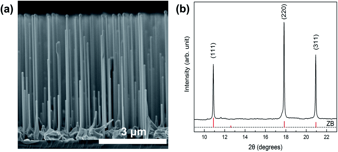 | ||
| Fig. 1 (a) Side-view SEM image of GaAs NWs grown on the Si (111) substrate by MBE. (b) XRD pattern of GaAs NWs (black) at ambient pressure compared with the peak positions of zinc blende structure (red ticks at the bottom correspond to the diffraction peaks of GaAs taken from JCPDs card, no. 80-0016). | ||
Fig. 2(a) presents the PL spectra of GaAs NWs with nitrogen as the PTM upon compression to 4.8 GPa. The photon energy and PL intensity show strong pressure-dependent behaviors. On the one hand, the PL peak energy exhibits a blue shift with pressure gradually. The light emission of GaAs NWs originates from the interband carrier recombination, so the blue-shifted peak energy indicates the pressure-induced broadening of the band gap. According to the linear-fitted pressure dependence curve shown in Fig. 2(b), the band gap evolution of GaAs can be approximated with the linear equation, Eg (eV) = 1.432 + 0.099P (P ≤ 4.8 GPa), consistent with a previous report.19 On the other hand, the PL intensity shows a dramatic increase with pressure up to 2.2 GPa, at which pressure there is a more than 30 fold enhancement compared with that at atmospheric pressure. However, with further compression above 2.2 GPa, the PL intensity decreases with pressure suddenly. This abrupt decrease behavior is in good agreement with the band gap transition from direct to indirect around 3 GPa, which has been demonstrated in both bulk and nanoscale GaAs in previous studies.19,22
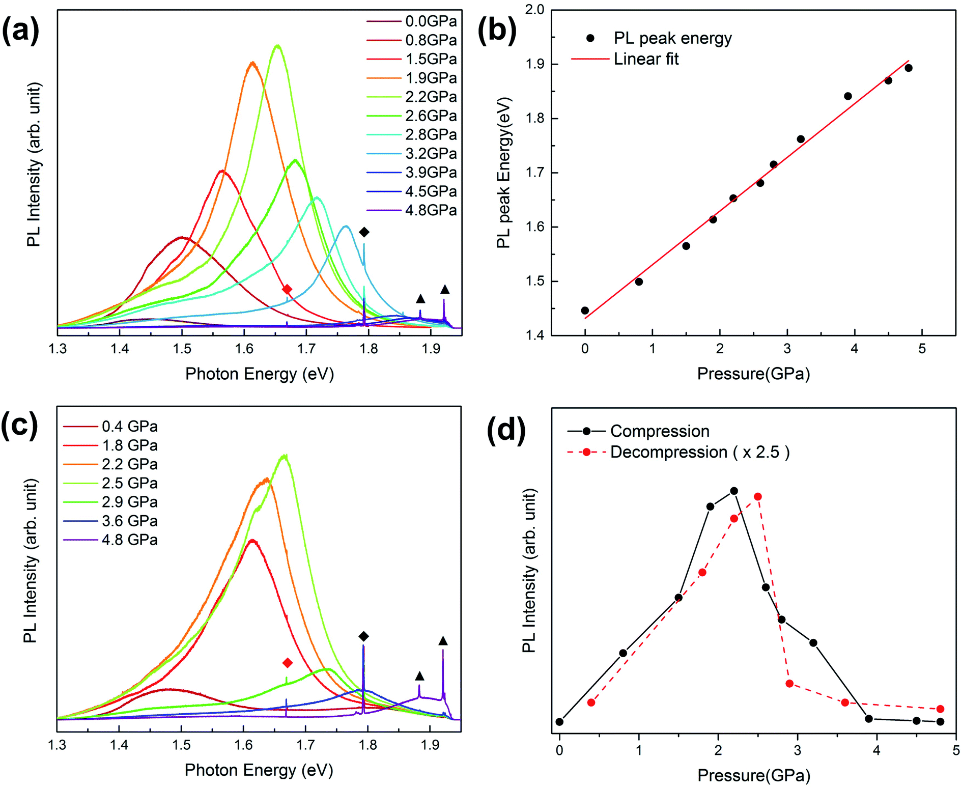 | ||
| Fig. 2 (a) PL spectra of GaAs NWs immersed in the nitrogen PTM at high pressure upon compression from 0 GPa to 4.8 GPa. (b) Peak energy evolution of PL peaks fitting as a function of pressure upon compression from 0 GPa to 4.8 GPa. (c) PL spectra of GaAs NWs immersed in the nitrogen PTM at high pressure upon decompression down to 0.4 GPa. (c) PL spectra of GaAs NWs without the PTM at high pressure upon compression from 0.4 GPa to 4.3 GPa. (d) Pressure dependence of the PL intensity of GaAs NWs with nitrogen in compression (black solid circle) and decompression processes (red solid circle). The black triangles, black square, and red square represent the Raman modes of GaAs, the Raman mode of diamond and the Raman mode of nitrogen, respectively. | ||
For confirming the pressure effect on the light emission of GaAs NWs, PL spectra upon decompression are shown in Fig. 2(c). In the pressure range from 4.8 GPa down to 2.5 GPa, the PL intensity increases with releasing pressure. Below 2.5 GPa, the PL intensity decreases with releasing pressure. The pressure dependence of PL intensity upon decompression (multiplied by a factor of 2.5) is compared with that upon compression in Fig. 2(d). The decompression PL spectra show quite similar pressure-dependent behaviors as observed in the compression process except for the slight hysteresis of the critical pressure where the PL peak gets the greatest enhancement. The reversible PL enhancement phenomenon indicates that the pressure can effectively promote the light emission efficiency of GaAs NWs with the nitrogen PTM, which is quite different from the previous passivation strategy in GaAs through an irreversible chemical reaction.
In order to reveal if nitrogen is necessary in the PL enhancement of GaAs NWs under high pressure, PL measurements with no PTM were carried out and the obtained results are shown in Fig. 3(a). There is a blue shift of the PL peak with compression in GaAs NWs with no PTM. Additionally, the peak energy evolution of the PL peaks of GaAs NWs with no PTM is shown in Fig. S1.† It is evident that the pressure-induced broadening of the band gap can also be observed in GaAs NWs with no PTM. However, there is no PL enhancement phenomenon up to 2.2 GPa. Then, an evident decrease in the PL intensity happens above 2.2 GPa and is caused by the direct-indirect band gap transition. The pressure dependence of the PL intensity of GaAs NWs with nitrogen and with no PTM is illustrated in Fig. 3(b), respectively. Compared with the remarkable PL enhancement in GaAs NWs immersed in nitrogen, the PL spectra without the PTM, the intensity of which has been multiplied by a factor of 10, have quite lower intensity and show no evident pressure response in a similar pressure range. Thus, the light emission enhancement is highly correlated with the nitrogen PTM instead of pressure-modulated band gaps. The nitrogen is an important medium for the realization of pressure-induced emission enhancement in GaAs NWs.
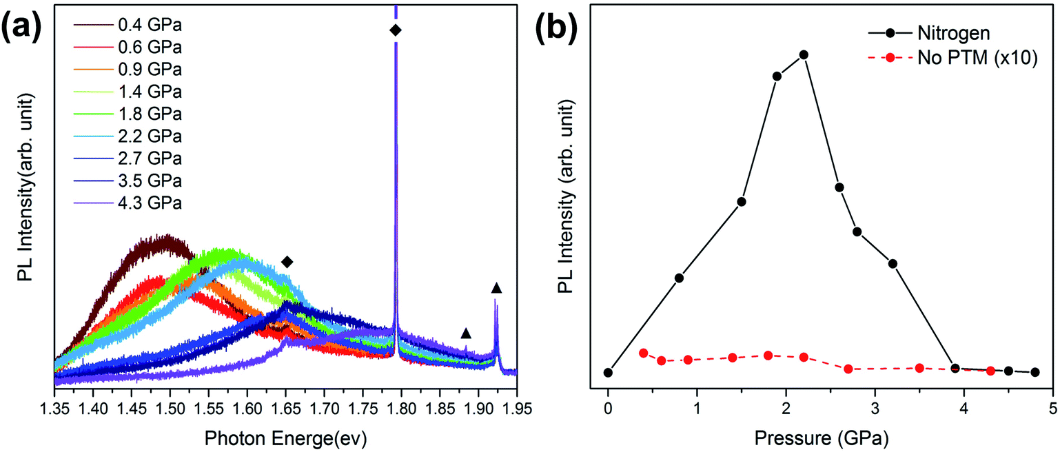 | ||
| Fig. 3 (a) PL spectra of GaAs NWs without the PTM at high pressure upon compression from 0.4 GPa to 4.3 GPa. The black triangles and black squares represent the Raman modes of GaAs and the Raman mode of diamond, respectively. (b) Pressure dependence of the PL intensity of GaAs NWs with nitrogen (black solid circles) and with no PTM (red solid circles). | ||
Nitrogen has already been applied as an efficient passivation element for suppressing the surface-related non-radiative recombination in GaAs NWs via forming a Ga–N compound.23,24 Due to the high stability of Ga–N bonds, nitridation induced PL enhancement in GaAs NWs has been demonstrated to be stable for a long time (more than 6 months) under atmospheric ambient conditions.24 However, in our experimental results, the PL enhancement disappears with quite low emission efficiency under atmospheric ambient conditions, which does not support the formation of the Ga–N compound on the surface of GaAs NWs. Furthermore, it is quite difficult to break the strong covalent bonds in the N2 molecule and induce the chemical reaction between GaAs and the N2 molecule under cold compression and Ga and N2 have been reported to form only GaN under high pressure with laser heating (1700–2800 K).25,26 In this work, a low power (∼2 mW) 633 nm laser was selected as the excitation source for avoiding the heating effect during the PL measurements. So the light emission enhancement observed in our experiment cannot be introduced by the chemical reactions reported in previous studies.23,24
For determining the interaction between N2 molecules and GaAs NWs, we calculated the electron localization function (ELF) of the N2@GaAs system under high pressure based on density functional theory (DFT). As shown in Fig. S2(a) and (c),† the ELF of the GaAs surface and N2 molecule is not connected with each other in the pressure range from 0 to 3 GPa. The sections of the ELF presented in Fig. S2(b) and (d)† further confirm that the electron located between the GaAs surface and N2 molecule is close to 0 (blue area) in the pressure range from 0 to 3 GPa. The ELF calculation results reveal no bond formation between N2 and GaAs, consistent with the reversible pressure-enhanced light emission phenomenon. However, in the pressure range of 0.8–2.2 GPa, the light emission of GaAs nanowires has already gotten evident enhancement, which indicates the efficient passivation in the same pressure range. Therefore, the nanowire surface passivation cannot originate from Ga–N bonds under N2 pressure.
Furthermore, first-principles calculations were also employed to explore the possible mechanism of pressure-induced emission enhancement in GaAs NWs. As shown in Fig. 4(a), the GaAs crystal surface is constructed with the N2 molecule located at the center. With a pressure of up to 2.0 GPa, the distance d between the N2 molecule and the GaAs surface decreases evidently as shown in Fig. 4(b). Pressure-dependence of the distance is illustrated in Fig. 4(c), and as pressure is applied on the N2@GaAs unit cell, the distance decreases with the pressure increase from 0 GPa to 3 GPa. Pressure can directly and efficiently reduce interatomic distances and change electronic orbitals, and a smaller distance means stronger interaction between the nitrogen molecule and the GaAs surface, which can affect the charge distribution of the N2@GaAs system. The electron density difference calculations under different pressures (0 GPa, 1 GPa, 2 GPa and 3 GPa) were carried out. As presented in Fig. 4(d) and (e), the purple and yellow colors indicate electron accumulation and electron depletion, respectively. Compared with the electron density difference of N2@GaAs at 0 GPa, there is more significant electron transfer from the GaAs layer to the N2 molecule at 2 GPa. The transferred charge quantity of the N2 molecule as a function of pressure is presented in Fig. 4(f) According to the calculation, the average charge transfer to per N2 molecule is 0.09 e from the GaAs surface at 0 GPa. With compression, the average charge transfer to the N2 molecule increases with pressure, such as 0.11 e (1 GPa), 0.38 e (2 GPa) and 0.48 e (3 GPa), which demonstrates the pressure-enhanced charge transfer effect.
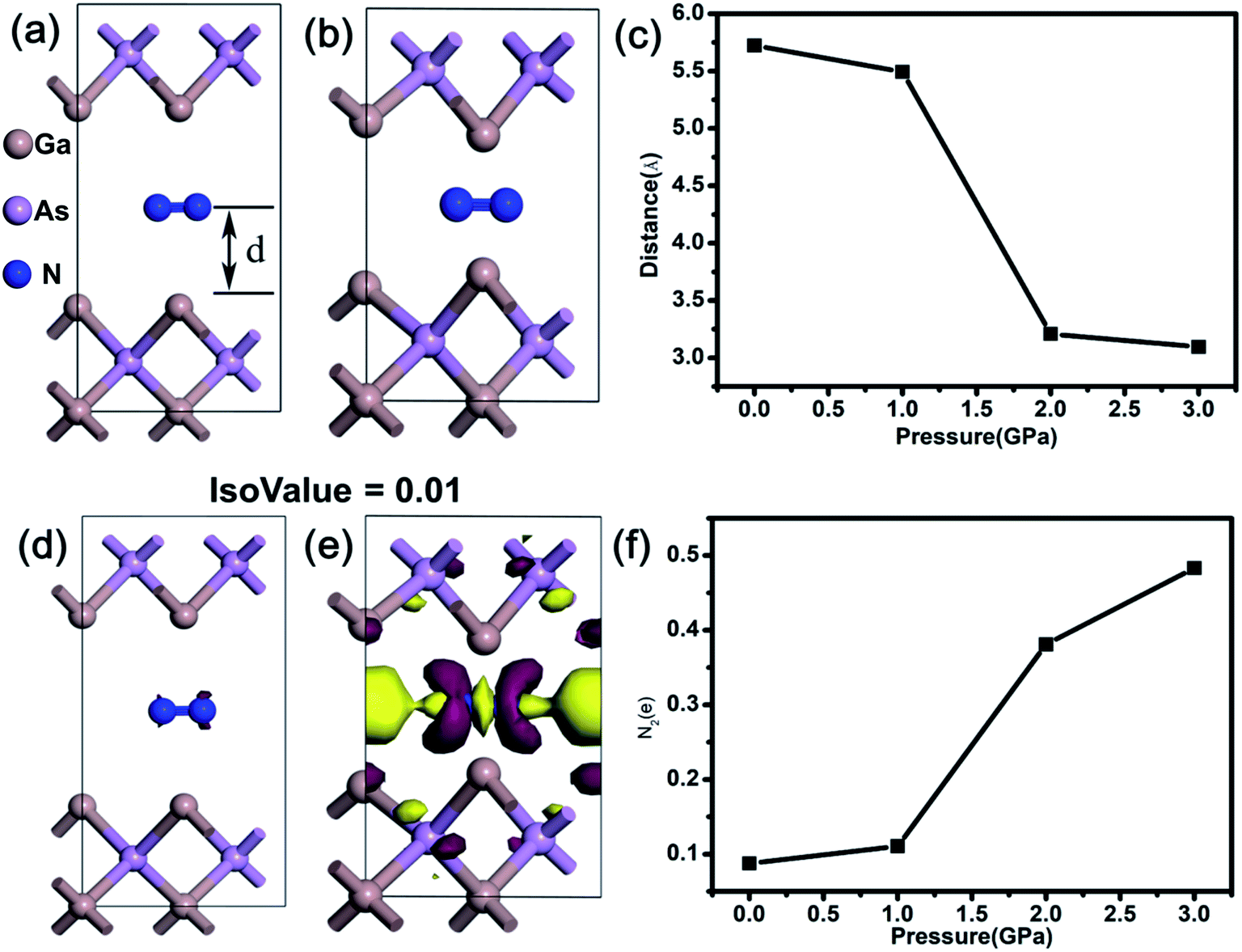 | ||
| Fig. 4 (a) N2@GaAs unit cell model at 0 GPa. d is the distance between the nitrogen molecule and the GaAs layer. (b) N2@GaAs unit cell model at 2 GPa. (c) Distance–pressure curve of selected pressure (0 GPa, 1 GPa, 2 GPa and 3 GPa). (d) Electron density difference of N2@GaAs at 0 GPa with an isovalue of 0.01. (e) Electron density difference of N2@GaAs at 2 GPa with an isovalue of 0.01. The purple and yellow colors indicate electron accumulation and electron depletion, respectively. (f) Transferred charge quantity as a function of pressure. | ||
The strong non-radiative surface recombination in GaAs NWs originates from the high density surface state. The surface dangling bonds of GaAs, which act as the non-radiative recombination centers, are responsible for the high density surface state. Sulfidation and nitridation have been proven to be efficient surface passivation methods for GaAs by forming GaAs-S and GaAs-N layers, respectively.24,27,28 In fact, along with the formation of the passivation layer, there is corresponding electron transfer from the GaAs surface atoms to S (N) atoms, which can effectively saturate the surface dangling bonds and reduce the non-radiative recombination centers. In addition, the charge transfer from the semiconductor surface to the adsorbed molecules has also been proven to reduce the density of the surface state in the study about C60 adsorption on the Si surface.29
In this work, the experimentally observed light emission enhancement demonstrates that the N2 molecules adsorbed on the surface atoms of GaAs can effectively passivate the surface states of GaAs NWs. And according to first principles calculations, compression reduces the interatomic distances and results in the enhanced charge transfer from the surface atoms of GaAs to N2 molecules, which will lead to the saturation of the surface dangling bonds and corresponding surface state passivation. Furthermore, the experimental PL emission intensity shows special pressure dependence (Fig. 2(d)), which is consistent with that of the calculated charge transfer quantity (Fig. 4(d)). Therefore, the pressure-enhanced electron transfer from the GaAs surface to N2 molecules, which can result in the reduction of surface state density, is responsible for the enhancement of light emission in GaAs NWs.
Conclusions
In summary, pressure-modulated light emission behaviors of zinc blende GaAs NWs have been investigated through the PL spectroscopic method in a DAC. The PL peak of GaAs NWs exhibits a blue shift with pressure gradually, and the corresponding approximate pressure coefficient is 99 meV/GPa up to 4.8 GPa. In the pressure range of 0–2.2 GPa, the PL intensity dramatically increases with pressure when GaAs NWs are immersed in nitrogen. Above 2.2 GPa, the band gap transition from direct to indirect induces the sudden decrease of light emission efficiency. The pressure-enhanced light emission of GaAs NWs is reversible in the decompression process. In contrast, there is no light emission enhancement effect in GaAs NWs without the PTM. The DFT calculation results reveal the pressure-enhanced charge transfer effect in the N2@GaAs system. The electron transfer from the GaAs surface to N2 molecules results in the reduction of the surface state and is responsible for light emission enhancement in GaAs NWs. This work provides insights into the mechanisms for pressure-modulated surface behaviors and a potential route for optimizing nanoscale functional devices.Conflicts of interest
There are no conflicts to declare.Acknowledgements
The synchrotron XRD measurement was performed at the BL15U1 beam line of the Shanghai Synchrotron Radiation Facility (SSRF). This work was supported by the National Key R&D Program of China (Grant No. 2018YFA0305900), the National Natural Science Foundation of China (Grant Nos. 11604116 and 61974138), the Beijing Municipal Natural Science Foundation, China (Grant No. 1192017), and the Youth Innovation Promotion Association, Chinese Academy of Sciences (Grant No. 2017156).Notes and references
- R. Yan, D. Gargas and P. Yang, Nat. Photonics, 2009, 3, 569–576 CrossRef CAS.
- A. Azhar, Y. X. Chen, V. Vasiraju and S. Vaddiraju, Nanotechnology, 2017, 28, 1–23 Search PubMed.
- Y. B. Wang, L. F. Wang, H. J. Joyce, Q. A. Gao, X. Z. Liao, Y. W. Mai, H. H. Tan, J. Zou, S. P. Ringer, H. J. Gao and C. Jagadish, Adv. Mater., 2011, 23, 1356–1360 CrossRef CAS PubMed.
- B. Hua, J. Motohisa, Y. Kobayashi, S. Hara and T. Fukui, Nano Lett., 2009, 9, 112–116 CrossRef CAS PubMed.
- S. Chen, M. Jansson, J. E. Stehr, Y. Huang, F. Ishikawa, W. M. Chen and I. A. Buyanova, Nano Lett., 2017, 17, 1775–1781 CrossRef CAS PubMed.
- D. Liang and J. E. Bowers, Nat. Photonics, 2010, 4, 511–517 CrossRef CAS.
- R. Chen, T. T. D. Tran, K. W. Ng, W. S. Ko, L. C. Chuang, F. G. Sedgwick and C. Chang-Hasnain, Nat. Photonics, 2011, 5, 170–175 CrossRef CAS.
- C. C. Chang, C. Y. Chi, M. Q. Yao, N. F. Huang, C. C. Chen, J. Theiss, A. W. Bushmaker, S. LaLumondiere, T. W. Yeh, M. L. Povinelli, C. W. Zhou, P. D. Dapkus and S. B. Cronin, Nano Lett., 2012, 12, 4484–4489 CrossRef CAS PubMed.
- D. Saxena, S. Mokkapati, P. Parkinson, N. Jiang, Q. Gao, H. H. Tan and C. Jagadish, Nat. Photonics, 2013, 7, 963–968 CrossRef CAS.
- J. Tatebayashi, S. Kako, J. F. Ho, Y. Ota, S. Iwamoto and Y. Arakawa, Nat. Photonics, 2015, 9, 501–506 CrossRef CAS.
- D. Saxena, N. A. Jiang, X. M. Yuan, S. Mokkapati, Y. A. Guo, H. H. Tan and C. Jagadish, Nano Lett., 2016, 16, 5080–5086 CrossRef CAS PubMed.
- T. Burgess, D. Saxena, S. Mokkapati, Z. Li, C. R. Hall, J. A. Davis, Y. D. Wang, L. M. Smith, L. Fu, P. Caroff, H. H. Tan and C. Jagadish, Nat. Commun., 2016, 7, 11927 CrossRef CAS PubMed.
- X. M. Yuan, L. Li, Z. Y. Li, F. Wang, N. Y. Wang, L. Fu, J. He, H. H. Tan and C. Jagadish, Nanoscale, 2019, 11, 9207 RSC.
- L. Zhang, Y. Wang, J. Lv and Y. M. Ma, Nat. Rev. Mater., 2017, 2, 17005 CrossRef CAS.
- X. P. Fu, F. F. Li, J. F. Lin, Y. B. Gong, X. L. Huang, Y. P. Huang, B. Han, Q. Zhou and T. Cui, J. Phys. Chem. Lett., 2017, 8, 3556–3563 CrossRef CAS PubMed.
- G. J. Xiao, Y. N. Wang, D. Han, K. X. Li, X. L. Feng, P. F. Lv, K. Wang, L. Liu, S. A. T. Redfern and B. Zou, J. Am. Chem. Soc., 2018, 140, 13970–13975 CrossRef CAS PubMed.
- W. Zhou, X. J. Chen, J. B. Zhang, X. H. Li, Y. Q. Wang and A. F. Goncharov, Sci. Rep., 2004, 4, 6472 CrossRef PubMed.
- Y. L. Liang, Z. Yao, X. T. Yin, P. Wang, L. X. Li, D. Pan, H. Y. Li, Q. J. Li, B. B. Liu and J. H. Zhao, Chin. Phys. B, 2019, 28, 076401 CrossRef CAS.
- I. Zardo, S. Yazji, C. Marini, E. Uccelli, A. F. I. Morral, G. Abstreiter and P. Postorino, ACS Nano, 2012, 6, 3284–3291 CrossRef CAS PubMed.
- S. Yang, K. Ding, X. M. Dou, X. F. Wu, Y. Yu, H. Q. Ni, Z. C. Niu, D. S. Jiang, S. S. Li and J. W. Luo, Phys. Rev. B: Condens. Matter Mater. Phys., 2015, 92, 165315 CrossRef.
- L. Li, D. Pan, Y. Xue, X. Wang, M. Lin, D. Su, Q. L. Zhang, X. Z. Yu, H. So, D. H. Wei, B. Q. Sun, P. H. Tan, A. L. Pan and J. H. Zhao, Nano Lett., 2017, 17, 622–630 CrossRef CAS PubMed.
- P. Y. Yu and B. Welber, Solid State Commun., 1978, 25, 209–211 CrossRef CAS.
- S. L. Chen, S. Filippov, F. Ishikawa, W. M. Chen and I. A. Buyanova, Appl. Phys. Lett., 2014, 105, 253106 CrossRef.
- P. A. Alekseev, M. S. Dunaevskiy, V. P. Ulin, T. V. Lvova, D. O. Filatov, A. V. Nezhdanov, A. I. Mashin and V. L. Berkovits, Nano Lett., 2015, 15, 63–68 CrossRef CAS PubMed.
- M. Hasegawa and T. Yagi, J. Cryst. Growth, 2000, 217, 349–354 CrossRef CAS.
- P. Perlin, I. Gorczyca, N. E. Christensen, I. Grzegory and T. Suski, Phys. Rev. B: Condens. Matter Mater. Phys., 1992, 45, 13307–13313 CrossRef CAS PubMed.
- V. N. Bessolov and M. V. Lebedev, Semiconductors, 1998, 32, 1141–1156 CrossRef.
- R. R. LaPierre, A. C. E. Chia, C. M. Haapamaki, N. Tajik, Y. Li, S. Zhao and Z. Mi, ECS Trans., 2012, 45, 51–60 CrossRef CAS.
- P. Moriarty, M. D. Upward, A. W. Dunn, Y.-R. Ma and P. H. Beton, Phys. Rev. B, 1998, 57, 362 CrossRef CAS.
Footnote |
| † Electronic supplementary information (ESI) available. See DOI: 10.1039/d0na00188k |
| This journal is © The Royal Society of Chemistry 2020 |