
 Open Access Article
 This Open Access Article is licensed under a Creative Commons Attribution-Non Commercial 3.0 Unported Licence
Formation of N2 bubbles along grain boundaries in (ZnO)1−x(GaN)x: nanoscale STEM-EELS studies†
Calliope
Bazioti
 *,
Vegard S.
Olsen
,
Andrej Y.
Kuznetsov
,
Lasse
Vines
and
Øystein
Prytz
*,
Vegard S.
Olsen
,
Andrej Y.
Kuznetsov
,
Lasse
Vines
and
Øystein
Prytz
Department of Physics, Centre for Materials Science and Nanotechnology, University of Oslo, PO Box 1048, Blindern, N-0316 Oslo, Norway. E-mail: kalliopi.bazioti@smn.uio.no
First published on 31st January 2020
Abstract
Direct evidence of N2 formation after annealing of (ZnO)1−x(GaN)x alloys was revealed. N2 was trapped by VZn+Ga-clusters, forming faceted voids along grain boundaries. This study shows that N–N bonding is a competitive path for nitrogen after annealing, in addition to the increasing Ga–N bonds, indicating that N in O substitution sites (NO) is not a stable configuration.
(ZnO)1−x(GaN)x (ZOGN) alloys are intriguing candidates for bandgap engineering, since the bandgap energy (Eg) of the system is reduced in comparison to its binary compounds (EZnOg ∼ 3.3 eV, EGaNg ∼ 3.4 eV) due to a strong band bowing effect.1 By tuning the alloy composition (x), Eg can be tailored from the UV-range into the visible part of the spectrum, making ZOGN a strong candidate for photovoltaic2,3 and solar water-splitting4–6 applications. However, the overall micro and nano-structure can strongly affect the semiconductor properties and device performance.7,8 In particular, the presence of grain boundaries and segregation of point defects along them has been linked to potential-barrier variations in polycrystalline ZnO, and variations in dislocation density have been related to changes in the photoluminescence spectra of ZnO.9–12 Moreover, chemically induced phenomena such as phase separation and elemental clustering can play a detrimental role in the functional properties of an alloy system. Post-deposition annealing usually improves the crystalline quality13–16 and recently Olsen et al.2,17,18 conducted a comprehensive study on magnetron sputtered ZnO-rich ZOGN thin films, elucidating the influence of composition and post-deposition annealing on the film properties, as well as investigating the mechanisms governing the band bowing effect. In the same study,17 DFT calculations revealed that the total energy of the system decreased by increasing the amount of Ga–N bonds, predicting a re-arrangement of the nitrogen bonds during post-deposition annealing. However, the behaviour of N in these alloys is not yet understood, and the proposed Ga–N bonds are not confirmed, warranting a detailed analysis on the nanoscopic scale.
In the present work, a detailed nanoscale investigation was conducted for the first time on magnetron sputtered (ZnO)0.85(GaN)0.15 thin films deposited on (0001) α-Al2O3 substrates. In this respect, (Scanning) Transmission Electron Microscopy ((S)TEM) was employed, combined with Electron Energy-Loss Spectroscopy (EELS) and Energy-Dispersive X-ray spectroscopy (EDX). Taking advantage of the possibility to use multiple detectors simultaneously, a direct correlation of the atomic structure to chemical information and bonding type gave valuable insight into the elemental and bonding distribution on the atomic scale and its correlation to defects. The influence of post-deposition annealing was investigated, as well as the impact of variations in the N2 gas flow during sputter deposition.
The formation of single-domain thin films exhibiting columnar grain structure was illustrated (S1, ESI†). (S)TEM imaging before and after annealing, showed an increase in the width of the grains, as well as a reduction in the threading dislocation (TD) density. EDX analysis on the meso-scale showed that the films are random alloys, exhibiting a homogeneous elemental distribution (S2, ESI†).
Despite this meso-scale improvement of the crystalline quality of the films, thermally induced nano-sized volumes were detected on the nano-scale. STEM-imaging was conducted using simultaneously high-angle annular dark field (HAADF), annular dark field (ADF) and annular bright field (ABF) detectors, to obtain complementary views of these volumes. Fig. 1a presents an ADF-STEM image showing a thin area of the film after annealing. Nano-sized areas exhibiting darker contrast are observed, preferentially formed along grain boundaries and TDs. High-resolution ADF-STEM images recorded along the [1![[1 with combining macron]](https://www.rsc.org/images/entities/char_0031_0304.gif) 00] and [11
00] and [11![[2 with combining macron]](https://www.rsc.org/images/entities/char_0032_0304.gif) 0] zone axes (Fig. 1b and c) illustrate a close-up of these regions, with a size ranging from ∼5 to ∼10 nm. These areas are not amorphous and there is no structural change observed, since the ABABAB stacking sequence of the hexagonal structure along the [0001] direction is retained. Moreover, imaging did not reveal any Moiré fringes. Evidently, these regions are surrounded by well-defined facets mainly on semi-polar planes ({101}, {112}), along with truncations on the polar {0001} planes. The enlarged insets are the corresponding HAADF and ABF images of the area annotated by the blue box in Fig. 1c. By resolving the Zn–O dumbbells, the polarity of the films is identified as Zn-faced (growth along the [0001] direction), indicating that the O-terminated internal polar facets of these regions are more stable, compared to the Zn-terminated polar facets (also S3, ESI†). Accounting that in HAADF-STEM imaging (S4, ESI†), contrast depends on Z and at high collection angles is formed by scattering from heavy elements, these dark regions indicate volumes with lower atomic density and their formation is attributed to agglomeration of vacancies (V).19 Since the concentration of Zn in the alloy is ∼85 at%, agglomeration of Zn-vacancies (VZn) is expected to contribute more in the formation of these volumes, however we cannot exclude a smaller contribution of Ga-vacancies (VGa) as well. Indeed, EDX-STEM maps of a lower-contrast volume, showed a reduction in both Zn and Ga counts (Fig. 1d). Elemental quantification extracted by EDX line profiles crossing these volumes showed no changes in the relative at% ratio between Zn and Ga, indicating no phase separation phenomena and no elemental clustering. Based on the size and lower atomic density of these areas, we hereafter label them nano-sized voids.
0] zone axes (Fig. 1b and c) illustrate a close-up of these regions, with a size ranging from ∼5 to ∼10 nm. These areas are not amorphous and there is no structural change observed, since the ABABAB stacking sequence of the hexagonal structure along the [0001] direction is retained. Moreover, imaging did not reveal any Moiré fringes. Evidently, these regions are surrounded by well-defined facets mainly on semi-polar planes ({101}, {112}), along with truncations on the polar {0001} planes. The enlarged insets are the corresponding HAADF and ABF images of the area annotated by the blue box in Fig. 1c. By resolving the Zn–O dumbbells, the polarity of the films is identified as Zn-faced (growth along the [0001] direction), indicating that the O-terminated internal polar facets of these regions are more stable, compared to the Zn-terminated polar facets (also S3, ESI†). Accounting that in HAADF-STEM imaging (S4, ESI†), contrast depends on Z and at high collection angles is formed by scattering from heavy elements, these dark regions indicate volumes with lower atomic density and their formation is attributed to agglomeration of vacancies (V).19 Since the concentration of Zn in the alloy is ∼85 at%, agglomeration of Zn-vacancies (VZn) is expected to contribute more in the formation of these volumes, however we cannot exclude a smaller contribution of Ga-vacancies (VGa) as well. Indeed, EDX-STEM maps of a lower-contrast volume, showed a reduction in both Zn and Ga counts (Fig. 1d). Elemental quantification extracted by EDX line profiles crossing these volumes showed no changes in the relative at% ratio between Zn and Ga, indicating no phase separation phenomena and no elemental clustering. Based on the size and lower atomic density of these areas, we hereafter label them nano-sized voids.
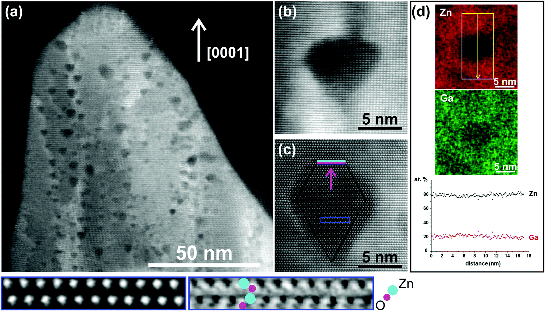 | ||
| Fig. 1 (a) ADF-STEM image, showing formation of thermally-induced nano-sized voids along grain boundaries and threading dislocations. (b) and (c) High-resolution ADF-STEM images along the [100] and [110] zone axes respectively, illustrating that the voids are not amorphous areas and they are surrounded by well-defined facets. The enlarged insets of the area annotated by the blue box show the corresponding HAADF and ABF images recorded simultaneously. By resolving the Zn–O dumbbells the polarity was identified showing that only the O-terminated internal polar facets are stabilized (purple line) along with the semi-polar facets (black lines). (d) EDX maps carried out in STEM-mode, show a reduction in both Zn and Ga counts and the void formation is attributed to agglomeration of Zn-vacancies (VZn) and Ga-vacancies (VGa). It is important that elemental quantification extracted by EDX line profiles crossing the voids, showed no changes in the relative at% ratio between Ga and Zn, indicating no phase separation phenomena or elemental clustering. | ||
Hence, EDX-STEM that is sensitive for the detection of heavy elements revealed no inhomogeneities in Zn and Ga distribution in both meso and nano-scale. However EDX is not ideal for the analysis of light elements due to the low fluorescence yield (less X-rays are produced because the formation of Auger electrons is favoured) and due to the background X-ray (Bremsstrahlung). Therefore, for the detection of light elements we employed EELS in STEM-mode that offers superior spatial and energy resolution and enables access to chemical bonding information. Fig. 2 shows a high-resolution ADF-STEM image (inset) where EELS spectra of the N–K and O–K edges were acquired by 2D scans from (1) a void and (2) the surrounding ZOGN matrix. EELS revealed that these voids are N-rich regions. Moreover, the shape and energy-position of the N–K edge indicate the presence of molecular nitrogen (N2), as shown by the comparison with N2 reference spectra.20 EELS spectra acquired from the ZOGN matrix revealed a different shape of the N–K peak compared to that of N2, indicating that N is bonded to the metal atoms. A comparison with spectra from a wz-GaN reference sample indicates that the Ga–N bonds proposed by DFT17 are also present. It should be clarified that the shape of spectrum 1 is the result of overlapped signals along the beam path (void + the surrounding ZOGN matrix).
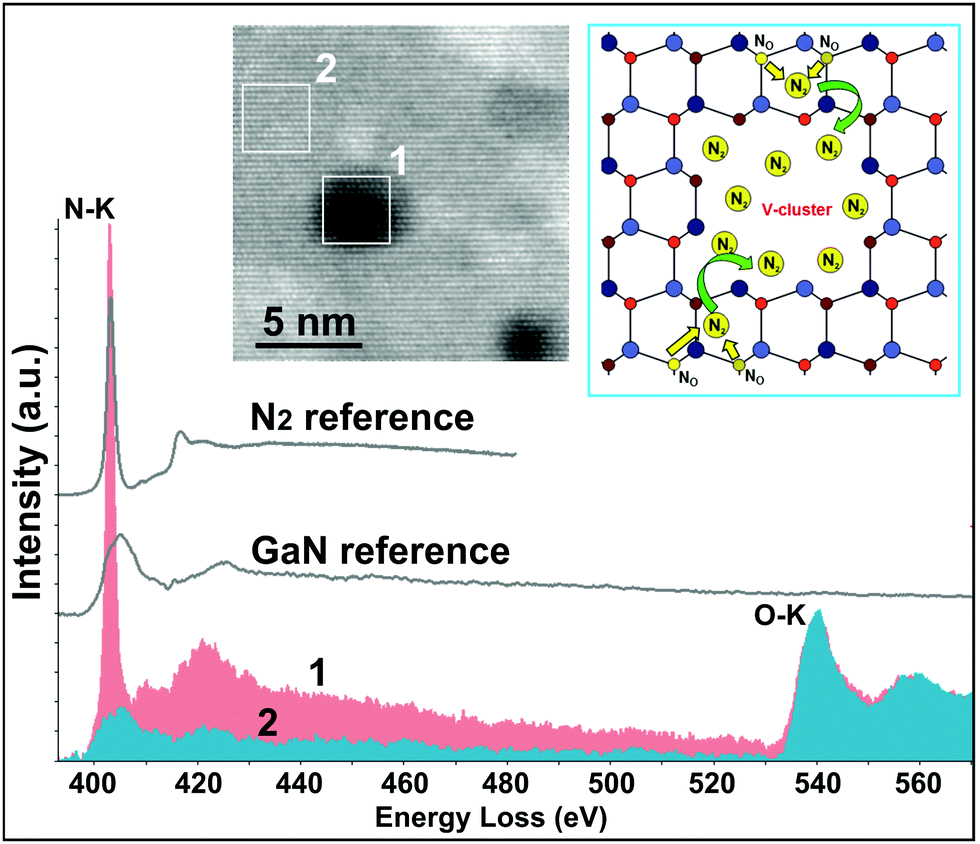 | ||
| Fig. 2 EELS-spectra acquired from 2D scans (1) inside a void and (2) the surrounding matrix, as annotated in the high-resolution STEM image (inset). Voids are N-rich regions and the shape and energy-position of the N–K edge indicate the existence of N–N bonds in the voids along with Ga–N bonds in the ZOGN matrix. A second inset shows a model describing the NO instability, formation of N2 molecules and trapping by V-clusters. | ||
A time resolved electron beam irradiation experiment was also performed in order to drill a hole in situ at the position of a void, while simultaneously recording an EELS spectrum every 0.5 s. A focused electron beam of sub-Å diameter and 350 pA current was used. Fig. 3a and b show ADF-STEM images of a void before and after the hole-drilling, respectively. The intensity ratio of the N–K/O–K peaks decreases abruptly after irradiation for 70 s (Fig. 3c), indicating a sudden removal of N2. After the release of the N2-bubble, the O–K peak is still present, indicating that there is still ZOGN matrix left. For ease of comparison, the EELS spectra were normalized to the O–K edge.
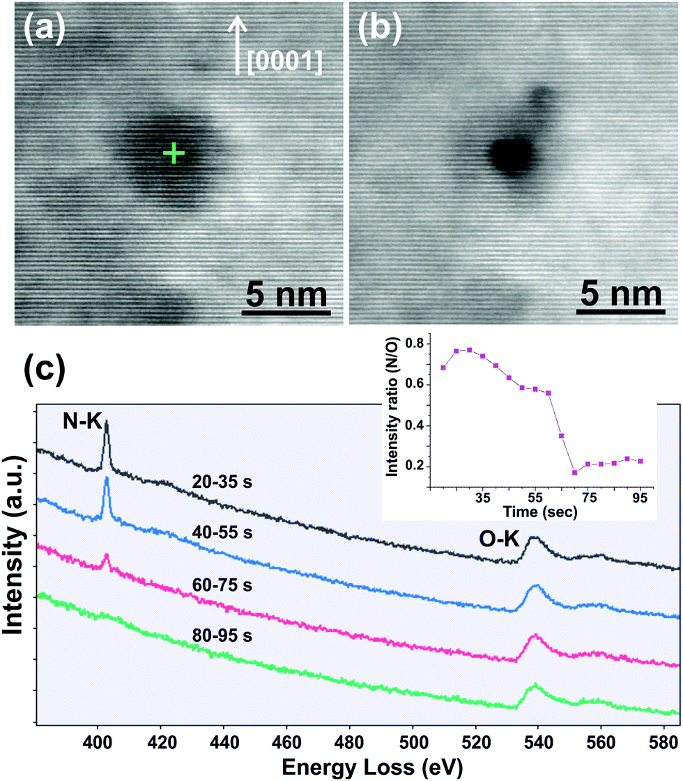 | ||
| Fig. 3 (a) and (b) ADF-STEM images of a N2-filled void recorded before and after drilling a hole in situ using a focused electron beam. (c) Time resolved EELS spectra acquired while drilling the hole, showing an abrupt decrease in the intensity ratio of N–K/O–K peaks after 70 s. After the release of the N2-bubble, the O–K peak is still present, indicating that there is still ZOGN matrix left. | ||
In addition to the post-annealing effect, we also examined the influence of the N2 gas flow that is applied during film deposition. In this respect, we studied annealed ZOGN films that were deposited under the same conditions but with reduced N2 gas flow (from 5 to 2.5 sccm). Nano-sized voids along grain boundaries and threading dislocations are still present, however EELS spectra reveal a significantly lower N–K signal (or absence of N–K signal), indicating that less N has been incorporated in the films and therefore trapped by the voids (non-stoichiometric conditions). The empty voids are found to be sharply faceted even at small sizes, while the N2-filled voids are more round and the well-defined facets appear as the voids grow in size (S5, ESI†). Furthermore, the O-terminated internal polar facets disappear as the voids grow in size and only the semi-polar facets ({101}, {112}) prevail.
This study shows that post-deposition thermal annealing results in a meso-scale crystal quality enhancement, as revealed by the grain enlargement and the TD-density reduction. However, in addition to the aforementioned line defects, a high concentration of point defects is expected (vacancies and atoms at interstitial positions) and our study goes further in terms of the comprehensive picture regarding the elemental distribution and bonding arrangement on the nano-scale. In particular, our results showing that after annealing large amounts of nitrogen are trapped by the voids as N2, indicate that N is not stable on the O substitutional site (NO). NO would be easily kicked out to an interstitial site (Ni) and due to the large Ni–Ni binding energy, N2 molecules can easily form.21 At the same time upon annealing, agglomeration of Zn-vacancies (VZn) and Ga-vacancies (VGa) along grain boundaries and TDs occurs. These vacancy-clusters act as traps for N2 molecules and gradually grow in size, ultimately forming faceted nano-voids. Nijikovsky et al.19 suggested that void formation can also be facilitated by pipe diffusion of the generated vacancies through dislocations that define the low-angle grain boundaries. After exceeding a critical size, the voids reach an equilibrium shape in order to minimize their energy state. This shape is determined by the surface energy of different facets. In our study the voids exhibited an asymmetric diamond shape related to the different surface energy for facets of opposite polarity. In particular, the O-terminated internal polar facets are more stable than the Zn-terminated, in agreement with previous observations.22 This polar facet disappears as the voids grow in size and finally only the semi-polar facets prevail. This is in agreement with calculations showing that the polar planes in ZnO exhibit higher surface formation energy compared to the non-polar planes.23,24 Trapping of large amounts of N at the voids leads to formation of overpressurized bubbles. Under the pressure of the accumulated gas, the N2-filled voids undergo plastic deformation, resulting in more rounded-shape facets. It should be emphasized that while our results show that large amounts of nitrogen are trapped in the voids as N2, there is also a significant amount of N in the ZOGN matrix, bonded to Ga and presumably Zn. This is also in agreement with our previous DFT calculations that suggest an increase in the number of Ga–N bonds after thermal treatment.17 However, the present study reveals that N–N bonding is an alternative path for nitrogen after annealing. It is also important that our results show that the increase in the Ga–N bonds did not lead to phase separation phenomena or clustering (e.g. GaN vs. ZnO phases). This means that our previously shown bandgap measurements on the nanoscale with EELS-STEM, are the result of a homogeneous alloy and not an average of a mixture of phases.18
Our findings support previous theoretical and experimental reports regarding the behaviour of N in ZnO. In particular, Fons et al.25 attributed the low p-type doping efficiency of N in ZnO to the low stability of NO, and showed the presence of N–N bonds by X-ray absorption experiments. DFT calculations by Gao et al.21 showed that NO can be easily deactivated to an interstitial site and form N–N bonds. Calculations by Nickel and Gluba26 showed that the O site is energetically unfavourable for the localization of N2, and calculations by Lambrecht and Boonchun27 showed that N2 may occupy a VZN site. However, these studies calculate energetics of single molecules in the lattice and X-ray absorption cannot provide information regarding the spatial distribution of the N-signal. In this study, STEM-EELS provides the advantage of both imaging and spectroscopy on the atomic scale, correlating simultaneously the atomic structure, chemical information and bonding type. Recently Bazioti et al.28 showed with STEM-EELS stabilization of VZn-clusters by N2 molecules and suppression of Vzn–Zni recombination in N-implanted ZnO after annealing.
In summary, the first comprehensive nanostructural and chemical report on magnetron sputtered ZOGN alloys was conducted. The elemental distribution and bonding re-arrangement was elucidated as a function of growth conditions and the evolution of thermally-induced defects was described. In particular, the meso-scale crystalline quality was improved after thermal annealing, as revealed by the enlargement of grains and the reduction of threading dislocation density. However, nano-sized voids were formed mainly along grain boundaries and STEM-EELS analysis showed direct evidence of molecular nitrogen (N2) filling the voids, indicating that N is not stable on the O substitution site (NO). Their formation is attributed to N2-trapping by Vzn+Ga clusters that upon annealing further agglomerate ultimately forming nano-voids. The voids reached an equilibrium shape defined by the energetically favourable facets, mainly on the semi-polar planes and the O-terminated internal polar plane. This study reveals that the N–N bonding is an alternative path for nitrogen after annealing, in addition to the increase in the Ga–N bonds that reduces the total energy of the system. Despite this re-arrangement of N-bonds, no phase separation phenomena were observed (GaN vs. ZnO) indicating that the previously reported bandgap of the system is the result of a homogeneous ZOGN alloy and not an average of a mixture of different phases.
Conflicts of interest
There are no conflicts to declare.Acknowledgements
Research Council of Norway is acknowledged for support to the Norwegian Center for Transmission Electron Microscopy (NORTEM) (no. 197405/F50), the top-tier research project FUNDAMeNT (no. 251131), the Norwegian Micro and Nano-Fabrication Facility (NorFab) (no. 245963/F50) and the SALIENT project (no. 239895).Notes and references
- K. Maeda, K. Teramura, D. Lu, T. Takata, N. Saito, Y. Inoue and K. Domen, Nature, 2006, 440, 295 CrossRef CAS PubMed.
- V. S. Olsen, C. Bazioti, A. Azarov, B. G. Svensson, A. Kuznetsov, Ø. Prytz and L. Vines, Semicond. Sci. Technol., 2019, 34, 1 CrossRef.
- C. Yang, Y. Hirose, T. Wakasugi, N. Kashiwa, H. Kawai, K. Yamashita and T. Hasegawa, Phys. Rev. Appl., 2018, 10, 1 Search PubMed.
- K. Maeda, K. Teramura, T. Takata, M. Hara, N. Saito, K. Toda, Y. Inoue, H. Kobayashi and K. Domen, J. Phys. Chem. B, 2005, 109, 20504 CrossRef CAS PubMed.
- K. Maeda and K. Domen, Chem. Mater., 2010, 22, 612 CrossRef CAS.
- H. Chen, L. Wang, J. Bai, J. C. Hanson, J. B. Warren, J. T. Muckerman, E. Fujita and J. A. Rodriguez, J. Phys. Chem. C, 2010, 114, 1809 CrossRef CAS.
- D. B. Holt and B. G. Yacobi, Extended Defects in Semiconductors, Cambridge University Press, Cambridge, 2007 Search PubMed.
- H. J. Queisser and E. E. Haller, Science, 1998, 281(5379), 945 CrossRef CAS PubMed.
- Y. Ohno, H. Koizumi, T. Taishi, I. Yonenaga, K. Fujii, H. Goto and T. Yao, J. Appl. Phys., 2008, 104(7), 073515 CrossRef.
- W. R. Liu, W. F. Hsieh, C. H. Hsu, K. S. Liang and F. S. S. Chien, J. Cryst. Growth, 2006, 297(2), 294 CrossRef CAS.
- M. A. McCoy, R. W. Grimes and W. E. Lee, J. Mater. Res., 1996, 11(8), 2009 CrossRef CAS.
- H. S. Domingos, P. D. Bristowe, J. Carlsson and B. Hellsing, Interface Sci., 2001, 9(3), 231 CrossRef CAS.
- S. R. Aghdaee and V. Soleimanian, J. Cryst. Growth, 2010, 312, 3050 CrossRef CAS.
- B. Y. Oh, M. C. Jeong, D. S. Kim, W. Lee and J. M. Myoung, J. Cryst. Growth, 2005, 281, 475 CrossRef CAS.
- B. D. Ahn, S. H. Oh, C. H. Lee, G. H. Kim, H. J. Kim and S. Y. Lee, J. Cryst. Growth, 2007, 309, 128 CrossRef CAS.
- S. Y. Kuo, W. C. Chen, F. I. Lai, C. P. Cheng, H. C. Kuo, S. C. Wang and W. F. Hsieh, J. Cryst. Growth, 2006, 287, 78 CrossRef CAS.
- V. S. Olsen, C. Bazioti, G. Baldissera, A. Azarov, Ø. Prytz, C. Persson, B. G. Svensson, A. Y. Kuznetsov and L. Vines, Phys. Status Solidi B, 2019, 1800529 CrossRef.
- V. S. Olsen, G. Baldissera, C. Zimmermann, C. S. Granerød, C. Bazioti, A. Galeckas, B. G. Svensson, A. Yu. Kuznetsov, C. Persson, Ø. Prytz and L. Vines, Phys. Rev. B: Condens. Matter Mater. Phys., 2019, 100, 165201 CrossRef CAS.
- B. Nijikovsky, J. J. Richardson, M. Garbrecht, S. P. DenBaars and W. D. Kaplan, J. Mater. Sci., 2013, 48, 1614 CrossRef CAS.
- A. Kovács, B. Schaffer, M. S. Moreno, J. R. Jinschek, A. J. Craven, T. Dietl, A. Bonanni and R. E. Dunin-Borkowski, J. Appl. Phys., 2013, 114, 033530 CrossRef.
- J. Gao, R. Qin, G. Luo, J. Lu, Y. Leprince-Wang, H. Ye, Z. Liao, Q. Zhao and D. Yu, Phys. Lett. A, 2010, 374, 3546 CrossRef CAS.
- K. S. Chan, L. Vines, L. Li, C. Jagadish, B. G. Svensson and J. Wong-Leung, Appl. Phys. Lett., 2015, 106, 212102 CrossRef.
- Y. J. Hong, J. Yoo, Y.-J. Doh, S. H. Kang, K.-j. Kong, M. Kim, D. R. Lee, K. H. Oh and G.-C. Yi, J. Mater. Chem., 2009, 19, 941 RSC.
- B. Meyer and D. Marx, Phys. Rev. B: Condens. Matter Mater. Phys., 2003, 67, 035403 CrossRef.
- P. Fons, H. Tampo, A. V. Kolobov, M. Ohkubo, S. Niki, J. Tominaga, R. Carboni and S. Friedrich, AIP Conf. Proc., 2007, 882, 381 CrossRef CAS.
- N. H. Nickel and M. A. Gluba, Phys. Rev. Lett., 2009, 103, 145501 CrossRef CAS PubMed.
- W. R. L. Lambrecht and A. Boonchun, Phys. Rev. B: Condens. Matter Mater. Phys., 2013, 87, 195207 CrossRef.
- C. Bazioti, A. Azarov, K. M. Johansen, B. G. Svensson, L. Vines, A. Y. Kuznetzov and Ø. Prytz, J. Phys. Chem. Lett., 2019, 10, 4725 CrossRef CAS PubMed.
Footnote |
| † Electronic supplementary information (ESI) available: Experimental methods employed including Magnetron Sputtering deposition, (Scanning) Transmission Electron Microscopy, Electron Energy-Loss Spectroscopy, TEM sample preparation, evaluation of sample thickness by low-loss EELS, Selected Area Diffraction Patterns, Weak-Beam Dark Field g/3g method, Energy-Dispersive X-ray spectroscopy meso-scale maps, simultaneous imaging with HAADF-ADF-ABF detectors, polarity investigation, and impact of changes in the N2 flow. See DOI: 10.1039/c9cp06025a |
| This journal is © the Owner Societies 2020 |