
 Open Access Article
 This Open Access Article is licensed under a Creative Commons Attribution-Non Commercial 3.0 Unported Licence
Selective electrochemical functionalization of the graphene edge†
Anur
Yadav
 ab,
Rodrigo M.
Iost
ab,
Tilmann J.
Neubert
abc,
Sema
Baylan
a,
Thomas
Schmid
ad and
Kannan
Balasubramanian
*abd
ab,
Rodrigo M.
Iost
ab,
Tilmann J.
Neubert
abc,
Sema
Baylan
a,
Thomas
Schmid
ad and
Kannan
Balasubramanian
*abd
aSchool of Analytical Sciences Adlershof (SALSA), Humboldt Universität zu Berlin, 10099 Berlin, Germany. E-mail: nano.anchem-at-hu-berlin.de
bDepartment of Chemistry, IRIS Adlershof, Humboldt Universität zu Berlin, 10099 Berlin, Germany
cHelmholtz-Zentrum Berlin für Materialien und Energie GmbH, Institut für Silizium-Photovolatik, Kekuléstr. 5, 12489 Berlin, Germany
dBAM, Federal Institute for Materials Research and Testing, Richard-Willstätter-Str. 11, 12489 Berlin, Germany
First published on 5th November 2018
Abstract
We present a versatile and simple method using electrochemistry for the exclusive functionalization of the edge of a graphene monolayer with metal nanoparticles or polymeric amino groups. The attachment of metal nanoparticles allows us to exploit surface-enhanced Raman scattering to characterize the chemistry of both the pristine and the functionalized graphene edge. For the pristine patterned graphene edge, we observe the typical edge-related modes, while for the functionalized graphene edge we identify the chemical structure of the functional layer by vibrational fingerprinting. The ability to obtain single selectively functionalized graphene edges routinely on an insulating substrate opens an avenue for exploring the effect of edge chemistry on graphene properties systematically.
Introduction
Graphene is the simplest stable atomically flat material that is being intensively investigated due to its unique physical and chemical properties.1–3 The chemistry of the interface between graphene and its environment (gas or liquid) plays a crucial role in the characteristic properties.4–7 Hence, it is important to devise methods to modify this chemistry precisely as well as to understand the effect of the modification on the ensuing properties, to engineer graphene for an application of interest.8,9 Many methods for modification of graphene in its various forms are currently pursued.10–14 As the surface dictates many properties of bulk materials, the edge of graphene is known to influence its electronic and chemical properties. The role played by the edges becomes dominant when narrowing down graphene sheets to nanoribbons, e.g. by lithographic patterning.15,16 The honeycomb lattice consists of different configurations of edges referred to as zigzag and armchair. Practically, however, combinations of both configurations are expected. The type of the edge determines the stability and the electronic structure.17–20 Graphene edges have been characterized using electrochemistry,21 Raman spectroscopy,22,23 and at atomic resolution using scanning probe microscopy24 and electron microscopy.25,26 Theoretically, the modification of the graphene edge is expected to modify the observed properties, such as oxygen groups modulating the electronic and magnetic properties of nanoribbons.20,27 Until now, most of the edge functionalization methods have been used on graphene flakes dispersed in solution, where a single object control and observation is not possible.28–32 There are two examples of chemical modification of the graphene edge carried out in the gas phase in ultrahigh vacuum at low temperatures. Using surface assisted coupling, tetrapyrroles were fused covalently to a graphene edge,33 while in another report individual tetrafluoro-tetracyanoquinodimethane molecules were fixed on the graphene edge by using an electronically inert molecular anchor.34 For both cases, the graphene edge was partially modified by using an elaborate and indirect methodology. The selective homogeneous modification of the edge of a single graphene sheet under ambient conditions has not been explored yet. Here we present a strategy to achieve this and at the same time gather spectroscopic information using the same construct, enabling us to corroborate the chemistry of the functional groups present or formed at the edge.Results and discussion
Fig. 1(a–c) presents a scheme with the general procedure for the exclusive chemical functionalization of the graphene edge (GrEdge). CVD-graphene is first transferred to Si/SiO2 substrates with pre-patterned electrodes using a wet transfer strategy.35 Polystyrene is used as a support polymer, which ensures minimal organic contamination.36 Following transfer, trace metal particles are removed using electrochemical etching (e-etching).37 (Details of fabrication are presented in the experimental section, and in ESI Fig. S1 and S2†). Following transfer, a positive photoresist is patterned using photolithography to define the location of the edge (Fig. 1(a)). The GrEdge is realized by removing the uncovered regions of the graphene sheet by a mild oxygen plasma treatment, leaving a neat exposed edge (Fig. 1(b)). The GrEdge is subsequently modified electrochemically using an appropriate precursor (Fig. 1(c)). The photoresist is an insulating layer of polymer that protects the graphene basal plane from coming in contact with the liquid, and ensures that a chemical reaction takes place exclusively at the GrEdge, which is the only part of the electrode exposed to the electrolyte solution. An absence of the photoresist will promote the electrochemistry reaction to occur at the whole surface of graphene and not only at the edge.38 The photoresist is finally removed in order to characterize the edge region. In the first example, the Au nanoparticles are deposited at the GrEdge through electrochemical reduction of a gold salt. Heterogeneous electron transfer between the gold species in solution (AuCl4−) and the GrEdge electrode results in the precipitation of gold at the edge.39 Specifically, a cathodic potential is applied (at the stage in Fig. 1(b)) in a solution of KAuCl4 (parameters in experimental section, and Fig. S3 in ESI†). Fig. 1(d) shows a large-scale scanning electron microscopy image and Fig. 1(e) an atomic force microscopy (AFM) image of the edge region (after removal of photoresist), where it is clear that a chain of particles are generated exclusively at the graphene edge. Support that the particles are gold is obtained from X-ray spectroscopic analysis (ESI, Fig. S4†). As a control, Fig. 1(f) presents an AFM image of a GrEdge sample obtained by the same procedure without any edge functionalization. From line profiles in such AFM images (Fig. S5†) we infer that the unmodified samples shows a clean graphene surface (with a height of around 1 nm), while the particles show an average height of 55 ± 7 nm. The particle size can in principle be varied by using different parameters for electrodeposition.40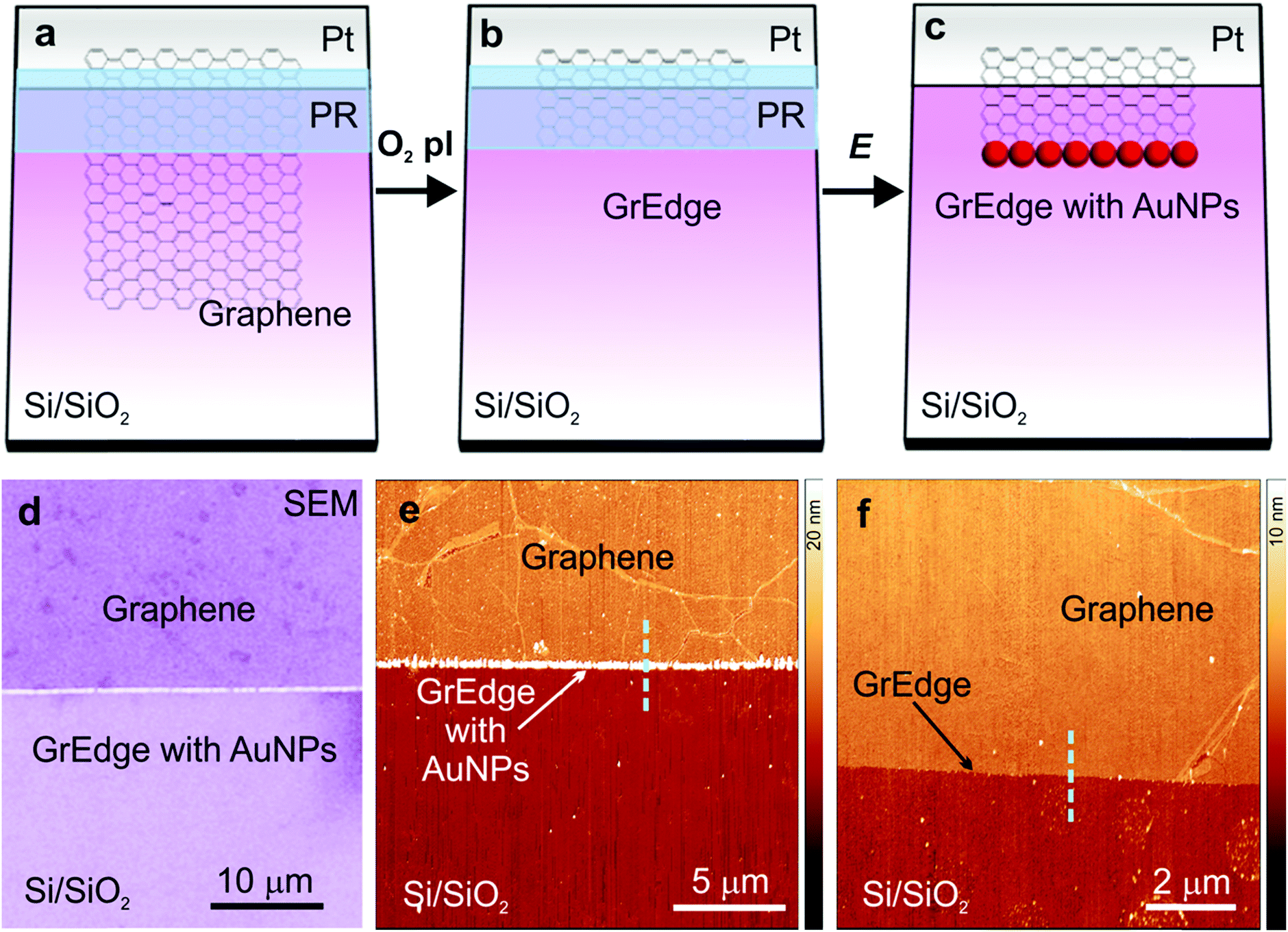 | ||
| Fig. 1 (a–c) Schematic of the procedure for fabrication and functionalization of a graphene edge (GrEdge): (a) patterning a photoresist layer (PR) on a graphene sheet on Si/SiO2 with pre-patterned electrode (Pt). (b) Etching uncovered graphene regions with O2 plasma (O2 pl) (c) electrodeposition of Au nanoparticles (AuNPs) at the GrEdge by application of a voltage (E) and dissolution of the photoresist. (d) Scanning electron microscope (SEM) image showing the modified GrEdge decorated with AuNPs. (e) AFM image of a GrEdge functionalized with AuNPs. (f) AFM image of a control sample with a non-functionalized edge. The cyan dashed lines have been used to extract line profiles shown in Fig. S5, ESI.† | ||
The deposition of AuNPs serves a twofold purpose. First, the exclusive deposition of particles at the edge can be confirmed by surface characterization as detailed above. Secondly, the presence of AuNPs at the edge allows us to perform selective spectroscopic characterization of the chemistry exclusively of the edge by virtue of surface enhanced Raman scattering (SERS).38,41 Raman spectroscopy is widely used to investigate the electronic and chemical properties of graphene.42–44 It is sensitive to the nature of graphene defects and edges, and has been used to monitor doping effects.45 In our case, the presence of particles at the GrEdge results in a surface enhancement exclusively at the edge and in this manner, the observed SERS signals can be associated as coming predominantly from the edge. Another important advantage of using AuNPs is that it allows for local vibrational mapping by SERS, which has enabled us in the past to obtain information about functional groups on the graphene surface.46 Hence, the construct can be directly used to investigate the presence or absence of functional groups at the patterned GrEdge.
Fig. 2(a) presents background-subtracted38 Raman spectra obtained at the basal plane, at the GrEdge without AuNPs and with AuNPs. Fig. 2(b) presents an AFM image of the GrEdge–AuNPs sample and the corresponding Raman maps (Fig. 2c, see Fig. S6 in ESI† for further analysis). For a better characterization of the edge, incident polarization was kept parallel to the edge, because the D-peak intensity strongly depends on the angle between incident polarization and edge.22 The Raman 2D map shows clearly that the intensity is relatively higher along the edge (indicative of SERS enhancement38,47), while the other Raman maps show that the disorder is exclusively observable at the edge.
 | ||
| Fig. 2 (a) Comparison of Raman spectra from the graphene basal plane (black curve), the graphene edge (red curve) and the graphene edge with AuNPs (blue curve). (b) AFM image of a GrEdge with AuNPs and (c) the corresponding Raman map of D′ (1620 cm−1), D (1330 cm−1, relative to G 1587 cm−1), and 2D (2653 cm−1) intensities (λex: 633 nm, 4.5 mW, 1 s). | ||
The spectrum of the basal plane (black curve) in Fig. 2(a) shows as expected only G and 2D peaks, indicative of graphene of high quality with minimal defects.45 The edge spectrum without AuNPs (red curve) shows additionally a small D-peak and a miniscule shoulder (D′-peak, ∼1620 cm−1) next to the G-peak. This is consistent with previous results, where both these signals are attributed to the presence of sp3-carbon, perturbing the honeycomb lattice and leading to an increase in the disorder-related D and D′ peaks of graphene.42,48–50 The D′ peak has been observed earlier on H-terminated zigzag graphene edges22,23,51 and in graphane (hydrogenated graphene).52–54 Interestingly, in the Raman spectrum of GrEdge–AuNPs (SERS spectrum), again only the same 4 peaks are visible, with a difference only in the relative intensities. The increase in the intensity of D-peak may be partly attributed to resonant enhancement by plasmonic absorption of the AuNPs at this energy.55 It is worth mentioning that when AuNPs are deposited on the basal plane, the D′-peak does not appear.38
Reactive plasma treatment is considered a possible source of generation of oxygenated chemical groups.56 In order to verify if we are sensitive to oxygen-related functional groups, we have deliberately oxidized a GrEdge electrochemically57 and subsequently attached the nanoparticles. In this case, we can observe additional oxygen-related peaks in the SERS spectra (ESI, Fig. S7†). Such oxygen-related peaks are however absent in the SERS spectra of the pristine GrEdge (Fig. 2(a)) suggesting that we have a rather low density of oxygen-related functional groups here. This is most likely due to the very mild plasma conditions used. Stronger plasma conditions are not suited since this would affect the photoresist adversely. The absence of oxygen-related groups at the edge has also been reported in other occasions, e.g. at the graphene edge under inert high vacuum conditions.25 SERS is known to be sensitive down to the single molecule level.47 It is worth mentioning that in the many 100 spectra (Fig. S8, ESI†) that were measured on the pristine GrEdge with varying particle sizes, we could only observe the edge related graphene modes. Hence, we conclude that the patterned edge is most likely predominantly hydrogen terminated, with a rather low density of other functionalities.
As a second example, we demonstrate the functionalization of the GrEdge with aromatic amino groups through oxidative electropolymerization of 4-aminobenzylamine (ABA). Similar to AuNPs, the deposition of ABA is also driven by heterogeneous electron transfer reaction between the ABA species in solution and GrEdge electrode. The electron transfer reaction promotes the irreversible oxidation of 4-ABA with the formation of a polymer layer containing oligomers of varying chain length58 at the GrEdge. This is achieved by performing two cycles of cyclic voltammetry (Fig. S9 in ESI†) with GrEdge at the stage of Fig. 1(b) as the working electrode in an aqueous solution of ABA. In order to characterize the attached functional groups in the realized poly(aminobenzylamine) (pABA) layer, the GrEdge–pABA is further modified with AuNPs using the same procedure as before. Since the polymer does not block electron transfer, it is still possible to reduce the gold species in solution.46 An AFM image of a typical GrEdge–pABA–AuNPs sample is shown in Fig. 3(a), while Fig. 3(b) presents typical Raman spectra at the functionalized GrEdge before (red curve) and after (blue curve) attachment of AuNPs. The spectrum of GrEdge–pABA–AuNPs shows new peaks in addition to the four graphene-related peaks, which we attribute to the vibrational fingerprint of the pABA layer. The negligible change in D peak intensity in the red spectrum indicates that pABA is non-covalently attached to GrEdge. This is consistent with reports on the oxidative coupling of substituted anilines (such as ABA) resulting in a non-covalent attachment of the polymer on carbon nanotubes39,59 and the graphene basal plane.46,60 This is also supported by the subsequent ability of the GrEdge–pABA to undergo electron transfer to obtain the AuNPs. By contrast, when the edge is functionalized with diazonium radicals (data not discussed here) – which is known to result in a covalent attachment – we were unable to obtain AuNPs at the GrEdge. This is consistent with covalently modified graphene showing much lower electron transfer rates.61
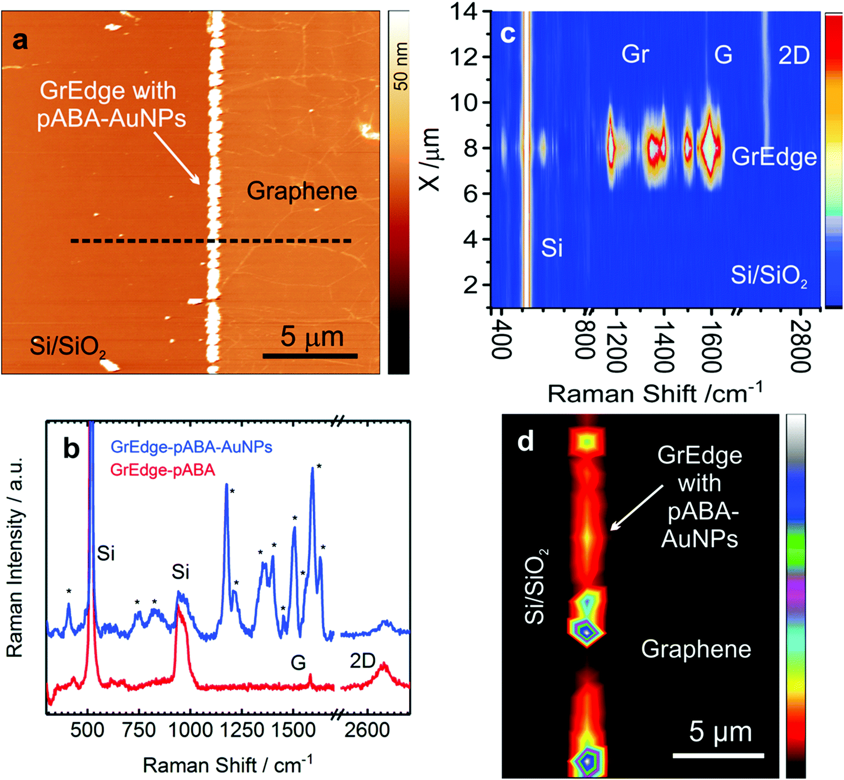 | ||
| Fig. 3 (a) AFM image of a typical GrEdge functionalized with poly(aminobenzylamine) (pABA) and AuNPs, referred to as GrEdge–pABA–AuNPs. (b) Comparison of the Raman spectra at GrEdge–pABA (red curve) and GrEdge–pABA–AuNPs (blue curve). (c) Raman map along the line shown in (a). (d) Map of the C–N stretching mode (1358 cm−1) of the same region as in (a) (λex: 633 nm, 3.4 mW, 2 × 1 s). | ||
Table 1 presents a summary of the assigned Raman modes for the peaks observed commonly in the spectra recorded at many positions on several samples (Fig. S10, ESI†). The Raman modes of pABA have some similarity with that of polyaniline due to their chemical structure.46,62,63 The mode at 1632 cm−1 is assigned to NH2 deformation characteristic of primary amine group,64 while the other modes at 1593 and 1566 cm−1 are due to C–C/C![[double bond, length as m-dash]](https://www.rsc.org/images/entities/char_e001.gif) C ring stretching of the benzenoid form.65 The occurrence of two bands at 1358 and 1399 cm−1 is attributed to C–N stretch.66 The mode at 1175 cm−1 is attributed to C–H bending. The band at around 1504 cm−1, arises from aromatic C–C stretching and a mode in low frequency region at 409 cm−1 is assigned to C–N–C bending of amines. The remaining modes at 1137 and 1214 cm−1, which are assigned to C–N stretch and C–C–N bending, may arise due to the free NH2 group, which is not participating in polymerization reaction.64 These characteristics of the Raman spectra of pABA confirm its formation at the GrEdge. A Raman map along a cross-section across the edge is shown in Fig. 3(c), where it is apparent that the pABA modes are found exclusively at the edge. This is further confirmed by the Raman map of the C–N stretching mode, as shown in Fig. 3(d). The spots corresponding to the vibrational modes of the pABA layer are elongated since the signals are convoluted by the diffraction-limited spot and the size of the nanoparticles.
C ring stretching of the benzenoid form.65 The occurrence of two bands at 1358 and 1399 cm−1 is attributed to C–N stretch.66 The mode at 1175 cm−1 is attributed to C–H bending. The band at around 1504 cm−1, arises from aromatic C–C stretching and a mode in low frequency region at 409 cm−1 is assigned to C–N–C bending of amines. The remaining modes at 1137 and 1214 cm−1, which are assigned to C–N stretch and C–C–N bending, may arise due to the free NH2 group, which is not participating in polymerization reaction.64 These characteristics of the Raman spectra of pABA confirm its formation at the GrEdge. A Raman map along a cross-section across the edge is shown in Fig. 3(c), where it is apparent that the pABA modes are found exclusively at the edge. This is further confirmed by the Raman map of the C–N stretching mode, as shown in Fig. 3(d). The spots corresponding to the vibrational modes of the pABA layer are elongated since the signals are convoluted by the diffraction-limited spot and the size of the nanoparticles.
| Raman shift (±2 cm−1) | Assigned peaks |
|---|---|
| 1632 | NH2 deformation |
| 1593 | CC ring stretch |
| 1566 | C–C ring stretch |
| 1504 | C–C ring stretch |
| 1453 | CH2 scissor vibration |
| 1400 | C–N stretch |
| 1358 | C–N stretch |
| 1214 | C–C–N bending |
| 1175 | C–H bending |
| 1137 | C–N stretch |
| 825 | C–H wag |
| 744 | C–N out of plane deformation |
| 409 | C–N–C bending |
Conclusions
In conclusion, we have demonstrated a versatile strategy for the realization of single functionalized graphene edges by selective and homogeneous non-covalent modification with Au nanoparticles or aromatic amino groups under ambient conditions on an insulating substrate. The presence of aromatic amino groups at the modified GrEdge could be corroborated by local vibrational fingerprinting. By varying the type of functional groups attached at the graphene edge, we can now tune this nanoscale interface in a versatile manner and systematically study its effect on the ensuing physical and chemical properties.Experimental
GrEdge devices
Ti/Pt (50 nm/10 nm) electrode lines were pre-patterned on Si with SiO2 (thickness of 500 nm) with 4-micron gaps using photolithography. The chips were cleaned in a piranha solution (H2SO4![[thin space (1/6-em)]](https://www.rsc.org/images/entities/char_2009.gif) :H2O2) (3:1) for 1 minute, and then in an oxygen plasma cleaner for 2 minutes before transfer of graphene. CVD grown-graphene-on-copper was cut into rectangular pieces (typically 2 cm × 2 cm) and a solution of poly(styrene) (PS) (50 mg mL−1 in toluene) was spotted over the CVD graphene foil as a polymer support and dried at 75 °C for 10 minutes. Then, the underlying copper was removed by etching in a solution of hydrochloric acid with added hydrogen peroxide (1.4 mol L−1 HCl + 0.5 mol L−1 H2O2) for 10 minutes. The PS/graphene slab was transferred to the Si/SiO2 chips with the pre-patterned Ti/Pt electrode lines and baked in an oven at 95 °C for 10 minutes before removal of PS in toluene (5 minutes with mechanical stirring). Finally, Si/SiO2/graphene chips were annealed at 600 °C under nitrogen atmosphere for 1 minute to improve the adhesion of graphene onto the silicon chips and remove possible residual organic contamination from the surface of the electrode. Prior to patterning of GrEdge electrodes, the removal of reminiscent copper particles was carried out by electrochemical etching (e-etching) in HCl 0.1 mol L−1, 15 scans in the potential range from −1 V to +0.1 V (vs. Ag/AgCl) at 50 mV s−1. The patterning of GrEdge was also done by photolithography (using a Maskless Aligner MLA-100, Heidelberg Instruments) followed by oxygen plasma etching. Specifically, a polymer layer of the commercial positive photoresist S1805 (Microposit) was spin-coated on top of the sample (∼500 nm thickness), pre-baked for 2:20 minutes at 90 °C and the negative of the desired area was exposed to light (λ = 365 nm). The photoresist from the exposed areas was removed by development using mf-319 developer (Microposit). The electrodes including contacted graphene are hence protected, with graphene being half protected and half exposed, separated by a sharp edge of the resist. The GrEdge was then obtained by exposure of non-protected graphene to oxygen plasma etching. For Raman spectroscopy and AFM imaging, the remaining photoresist was removed in acetone for 15 seconds.
:H2O2) (3:1) for 1 minute, and then in an oxygen plasma cleaner for 2 minutes before transfer of graphene. CVD grown-graphene-on-copper was cut into rectangular pieces (typically 2 cm × 2 cm) and a solution of poly(styrene) (PS) (50 mg mL−1 in toluene) was spotted over the CVD graphene foil as a polymer support and dried at 75 °C for 10 minutes. Then, the underlying copper was removed by etching in a solution of hydrochloric acid with added hydrogen peroxide (1.4 mol L−1 HCl + 0.5 mol L−1 H2O2) for 10 minutes. The PS/graphene slab was transferred to the Si/SiO2 chips with the pre-patterned Ti/Pt electrode lines and baked in an oven at 95 °C for 10 minutes before removal of PS in toluene (5 minutes with mechanical stirring). Finally, Si/SiO2/graphene chips were annealed at 600 °C under nitrogen atmosphere for 1 minute to improve the adhesion of graphene onto the silicon chips and remove possible residual organic contamination from the surface of the electrode. Prior to patterning of GrEdge electrodes, the removal of reminiscent copper particles was carried out by electrochemical etching (e-etching) in HCl 0.1 mol L−1, 15 scans in the potential range from −1 V to +0.1 V (vs. Ag/AgCl) at 50 mV s−1. The patterning of GrEdge was also done by photolithography (using a Maskless Aligner MLA-100, Heidelberg Instruments) followed by oxygen plasma etching. Specifically, a polymer layer of the commercial positive photoresist S1805 (Microposit) was spin-coated on top of the sample (∼500 nm thickness), pre-baked for 2:20 minutes at 90 °C and the negative of the desired area was exposed to light (λ = 365 nm). The photoresist from the exposed areas was removed by development using mf-319 developer (Microposit). The electrodes including contacted graphene are hence protected, with graphene being half protected and half exposed, separated by a sharp edge of the resist. The GrEdge was then obtained by exposure of non-protected graphene to oxygen plasma etching. For Raman spectroscopy and AFM imaging, the remaining photoresist was removed in acetone for 15 seconds.
Electrochemical setup
Electrochemical modification was carried out using a three-electrode system comprising of GrEdge as working electrode, platinum wire (Φ = 0.5 mm) as the auxiliary electrode and Ag/AgCl as the reference electrode. The experiments were performed in an electrochemical cell with 20 mL of solution using an Ivium Compacstat potentiostat.Electrochemical modification of GrEdge with AuNPs
The electrochemical modification was performed in the same electrochemical setup described above. GrEdge–AuNPs were obtained potentiostatically in four deposition steps as following: 0.4 V for 20 s, −0.5 V for 5 s, 0.4 V for 20 s and −0.5 V for 5 s (Fig. S3†). For GrEdge, the concentration of aqueous solution of gold metal salt and the background electrolyte for all the depositions were 10 μmol L−1 KAuCl4 and LiClO4 0.1 mol L−1.Electrochemical modification of GrEdge with pABA followed by AuNPs
For the functionalization of GrEdge with pABA, 4-aminobenzylamine (4-ABA) aqueous solution at a concentration of 5 mmol L−1 with 0.1 mol L−1 LiClO4 was polymerized using cyclic voltammetry at a potential range of −0.2 V to 0.8 V vs. Ag/AgCl for two cycles. Then, AuNPs arrays were deposited by chronoamperometry as described above by the use of 30 μmol L−1 KAuCl4 in 0.1 mol L−1 LiClO4. The gold salt solution was always prepared right before the electrochemical deposition experiments.Raman spectroscopy and AFM images
Raman spectra for GrEdge–AuNP electrodes were obtained on LabRam HR 800 equipped with a 1024 × 256 CCD detector (symphony; liquid N2 cooled), a 300 L mm−1 grating, a HeNe laser with an excitation wavelength of 632.8 nm, a 100 × (NA 0.90) objective, and a detection pinhole of 100 μm. The power was maintained at 4.5 mW for acquisitions on all the graphene samples. Raman spectra for GrEdge–pABA–AuNPs were obtained on a JASCO NRS-4100 Raman spectrometer equipped with a 1650 × 256 CCD detector (Andor; air/Peltier-cooled, operating temperature: −60 °C), a 400 L mm−1 grating, a diode laser with an excitation of 632.8 nm, and a 100× (NA 0.90) objective and a power of 3.4 mW. The Raman spectra and maps were recorded using LabSpec 6 for GrEdge–AuNPs electrodes and spectra manager for GrEdge–pABA–AuNPs. The spectrometer for both instruments was calibrated by determining the wavenumber position of Raman line of a silicon substrate at 520.7 cm−1 before data acquisition. Raman spectra and map images were processed using Origin 9.1. The Raman data was fitted with Lorentzian profile in Origin 9.1 or Mathematica to determine the peak position and FWHM. Raman maps were obtained by integrating the intensity in the range of ±10 cm−1 around the main peak. AFM images were obtained using a commercial Dimension IV working in tapping mode in the ambient. AFM images were processed using Gwyddion.Scanning electron microscopy (SEM) and energy dispersive X-ray spectroscopy (EDX)
SEM and EDX data were acquired using a JEOL JCM-6000 Neoscope ESEM-EDX instrument in high-vacuum mode (approx. 10–4 mbar). No coating or any other pretreatment was applied to the samples. The image shown in Fig. 1(d) is a secondary electron image, while for EDX, a rectangular area along the aligned nanoparticles was selected on a backscattered electron image for accumulation of the spectrum shown in Fig. S4, ESI.†Conflicts of interest
There are no conflicts to declare.Acknowledgements
AY thanks the funding from the German Science Foundation (DFG) via the Graduate School of Analytical Sciences Adlershof (SALSA GSC1013). RMI acknowledges CAPES/AvH-Foundation (Iost-CAPES-2017-18) for financial support.References
- A. K. Geim and K. S. Novoselov, Nat. Mater., 2007, 6, 183–191 CrossRef CAS PubMed.
- A. K. Geim, Science, 2009, 324, 1530 CrossRef CAS PubMed.
- K. S. Novoselov, A. K. Geim, S. V. Morozov, D. Jiang, Y. Zhang, S. V. Dubonos, I. V. Grigorieva and A. A. Firsov, Science, 2004, 306, 666 CrossRef CAS PubMed.
- F. Schedin, A. K. Geim, S. V. Morozov, E. W. Hill, P. Blake, M. I. Katsnelson and K. S. Novoselov, Nat. Mater., 2007, 6, 652 CrossRef CAS PubMed.
- Q. H. Wang, Z. Jin, K. K. Kim, A. J. Hilmer, G. L. C. Paulus, C.-J. Shih, M.-H. Ham, J. D. Sanchez-Yamagishi, K. Watanabe, T. Taniguchi, J. Kong, P. Jarillo-Herrero and M. S. Strano, Nat. Chem., 2012, 4, 724 CrossRef CAS PubMed.
- K. Yokota, K. Takai and T. Enoki, Nano Lett., 2011, 11, 3669–3675 CrossRef CAS PubMed.
- Z. Yan, Z. Sun, W. Lu, J. Yao, Y. Zhu and J. M. Tour, ACS Nano, 2011, 5, 1535–1540 CrossRef CAS PubMed.
- C. N. R. Rao, A. K. Sood, K. S. Subrahmanyam and A. Govindaraj, Angew. Chem., Int. Ed., 2009, 48, 7752–7777 CrossRef CAS PubMed.
- E. P. Randviir, D. A. C. Brownson and C. E. Banks, Mater. Today, 2014, 17, 426–432 CrossRef CAS.
- J. Greenwood, T. H. Phan, Y. Fujita, Z. Li, O. Ivasenko, W. Vanderlinden, H. Van Gorp, W. Frederickx, G. Lu, K. Tahara, Y. Tobe, I. H. Uji, S. F. Mertens and S. De Feyter, ACS Nano, 2015, 9, 5520–5535 CrossRef CAS PubMed.
- T. Kuila, S. Bose, A. K. Mishra, P. Khanra, N. H. Kim and J. H. Lee, Prog. Mater. Sci., 2012, 57, 1061–1105 CrossRef CAS.
- D. W. Boukhvalov and M. I. Katsnelson, J. Phys.: Condens. Matter, 2009, 21, 344205 CrossRef CAS PubMed.
- A. Hirsch, J. M. Englert and F. Hauke, Acc. Chem. Res., 2013, 46, 87–96 CrossRef CAS PubMed.
- C. K. Chua and M. Pumera, Chem. Soc. Rev., 2013, 42, 3222–3233 RSC.
- X. Wang and H. Dai, Nat. Chem., 2010, 2, 661–665 CrossRef CAS PubMed.
- M. Y. Han, B. Ozyilmaz, Y. Zhang and P. Kim, Phys. Rev. Lett., 2007, 98, 206805 CrossRef PubMed.
- X. Jia, M. Hofmann, V. Meunier, B. G. Sumpter, J. Campos-Delgado, J. M. Romo-Herrera, H. Son, Y.-P. Hsieh, A. Reina, J. Kong, M. Terrones and M. S. Dresselhaus, Science, 2009, 323, 1701 CrossRef CAS PubMed.
- A. Muge and J. C. Yves, Jpn. J. Appl. Phys., 2011, 50, 070101 CrossRef.
- K. A. Ritter and J. W. Lyding, Nat. Mater., 2009, 8, 235–242 CrossRef CAS PubMed.
- O. Hod, V. Barone, J. E. Peralta and G. E. Scuseria, Nano Lett., 2007, 7, 2295–2299 CrossRef CAS PubMed.
- W. Yuan, Y. Zhou, Y. Li, C. Li, H. Peng, J. Zhang, Z. Liu, L. Dai and G. Shi, Sci. Rep., 2013, 3, 2248 CrossRef PubMed.
- C. Casiraghi, A. Hartschuh, H. Qian, S. Piscanec, C. Georgi, A. Fasoli, K. S. Novoselov, D. M. Basko and A. C. Ferrari, Nano Lett., 2009, 9, 1433–1441 CrossRef CAS PubMed.
- A. K. Gupta, T. J. Russin, H. R. Gutierrez and P. C. Eklund, ACS Nano, 2009, 3, 45–52 CrossRef CAS PubMed.
- Y. F. Kobayashi, K.-I. Fukui and T. Enoki, Phys. Rev. B: Condens. Matter Mater. Phys., 2006, 73, 125415 CrossRef.
- K. Suenaga and M. Koshino, Nature, 2010, 468, 1088–1090 CrossRef CAS PubMed.
- Z. Liu, K. Suenaga, P. J. Harris and S. Iijima, Phys. Rev. Lett., 2009, 102, 015501 CrossRef PubMed.
- F. Cervantes-Sodi, G. Csányi, S. Piscanec and A. C. Ferrari, Phys. Rev. B: Condens. Matter Mater. Phys., 2008, 77, 165427 CrossRef.
- Z. Xiang, Q. Dai, J. F. Chen and L. Dai, Adv. Mater., 2016, 28, 6253–6261 CrossRef CAS PubMed.
- A. Shen, Y. Zou, Q. Wang, A. W. Dryfe Robert, X. Huang, S. Dou, L. Dai and S. Wang, Angew. Chem., Int. Ed., 2014, 53, 10804–10808 CrossRef CAS PubMed.
- I.-Y. Jeon, H.-J. Choi, S.-M. Jung, J.-M. Seo, M.-J. Kim, L. Dai and J.-B. Baek, J. Am. Chem. Soc., 2013, 135, 1386–1393 CrossRef CAS PubMed.
- J. Xu, J. Shui, J. Wang, M. Wang, H.-K. Liu, S. X. Dou, I.-Y. Jeon, J.-M. Seo, J.-B. Baek and L. Dai, ACS Nano, 2014, 8, 10920–10930 CrossRef CAS PubMed.
- M. Quintana, A. Montellano, A. E. del Rio Castillo, G. V. Tendeloo, C. Bittencourt and M. Prato, Chem. Commun., 2011, 47, 9330–9332 RSC.
- Y. He, M. Garnica, F. Bischoff, J. Ducke, M. L. Bocquet, M. Batzill, W. Auwarter and J. V. Barth, Nat. Chem., 2017, 9, 33–38 CrossRef CAS PubMed.
- S. Wickenburg, J. Lu, J. Lischner, H. Z. Tsai, A. A. Omrani, A. Riss, C. Karrasch, A. Bradley, H. S. Jung, R. Khajeh, D. Wong, K. Watanabe, T. Taniguchi, A. Zettl, A. H. Neto, S. G. Louie and M. F. Crommie, Nat. Commun., 2016, 7, 13553 CrossRef CAS PubMed.
- X. Li, W. Cai, J. An, S. Kim, J. Nah, D. Yang, R. Piner, A. Velamakanni, I. Jung, E. Tutuc, S. K. Banerjee, L. Colombo and R. S. Ruoff, Science, 2009, 324, 1312 CrossRef CAS PubMed.
- J. Song, F.-Y. Kam, R.-Q. Png, W.-L. Seah, J.-M. Zhuo, G.-K. Lim, P. K. H. Ho and L.-L. Chua, Nat. Nanotechnol., 2013, 8, 356 CrossRef CAS PubMed.
- M. Iost Rodrigo, N. Crespilho Frank, L. Zuccaro, K. Yu Hak, M. Wodtke Alec, K. Kern and K. Balasubramanian, ChemElectroChem, 2014, 1, 2070–2074 CrossRef.
- K. Balasubramanian, L. Zuccaro and K. Kern, Adv. Funct. Mater., 2014, 24, 6348–6358 CrossRef CAS.
- K. Balasubramanian and M. Burghard, J. Mater. Chem., 2008, 18, 3071–3083 RSC.
- M. Scolari, A. Mews, N. Fu, A. Myalitsin, T. Assmus, K. Balasubramanian, M. Burghard and K. Kern, J. Phys. Chem. C, 2008, 112, 391–396 CrossRef CAS.
- F. Schedin, E. Lidorikis, A. Lombardo, V. G. Kravets, A. K. Geim, A. N. Grigorenko, K. S. Novoselov and A. C. Ferrari, ACS Nano, 2010, 4, 5617–5626 CrossRef CAS PubMed.
- L. M. Malard, M. A. Pimenta, G. Dresselhaus and M. S. Dresselhaus, Phys. Rep., 2009, 473, 51–87 CrossRef CAS.
- Y. You, Z. Ni, T. Yu and Z. Shen, Appl. Phys. Lett., 2008, 93, 163112 CrossRef.
- M. Begliarbekov, O. Sul, S. Kalliakos, E.-H. Yang and S. Strauf, Appl. Phys. Lett., 2010, 97, 031908 CrossRef.
- A. C. Ferrari and D. M. Basko, Nat. Nanotechnol., 2013, 8, 235–246 CrossRef CAS PubMed.
- L. Zuccaro, K. Kern and K. Balasubramanian, ACS Nano, 2015, 9, 3314–3323 CrossRef CAS PubMed.
- K. Kneipp, H. Kneipp, I. Itzkan, R. R. Dasari and M. S. Feld, Chem. Rev., 1999, 99, 2957–2976 CrossRef CAS PubMed.
- D. M. Basko, S. Piscanec and A. C. Ferrari, Phys. Rev. B: Condens. Matter Mater. Phys., 2009, 80, 165413 CrossRef.
- S. Reich and C. Thomsen, Philos. Trans. R. Soc., A, 2004, 362, 2271–2288 CrossRef CAS PubMed.
- A. C. Ferrari, J. C. Meyer, V. Scardaci, C. Casiraghi, M. Lazzeri, F. Mauri, S. Piscanec, D. Jiang, K. S. Novoselov, S. Roth and A. K. Geim, Phys. Rev. Lett., 2006, 97, 187401 CrossRef CAS PubMed.
- R. Yang, Z. W. Shi, L. C. Zhang, D. X. Shi and G. Y. Zhang, Nano Lett., 2011, 11, 4083–4088 CrossRef CAS PubMed.
- D. C. Elias, R. R. Nair, T. M. G. Mohiuddin, S. V. Morozov, P. Blake, M. P. Halsall, A. C. Ferrari, D. W. Boukhvalov, M. I. Katsnelson, A. K. Geim and K. S. Novoselov, Science, 2009, 323, 610–613 CrossRef CAS PubMed.
- H. Sahin, O. Leenaerts, S. K. Singh and F. M. Peeters, Wiley Interdiscip. Rev.: Comput. Mol. Sci., 2015, 5, 255–272 CAS.
- Y. Wang, X. F. Xu, J. Lu, M. Lin, Q. L. Bao, B. Ozyilmaz and K. P. Loh, ACS Nano, 2010, 4, 6146–6152 CrossRef CAS PubMed.
- C. L. Haynes and R. P. Van Duyne, J. Phys. Chem. B, 2003, 107, 7426–7433 CrossRef CAS.
- A. Bottcher, M. Heil, N. Sturzl, S. S. Jester, S. Malik, F. Perez-Willard, P. Brenner, D. Gerthsen and M. M. Kappes, Nanotechnology, 2006, 17, 5889–5894 CrossRef.
- Y. Yi, G. Weinberg, M. Prenzel, M. Greiner, S. Heumann, S. Becker and R. Schlögl, Catal. Today, 2017, 295, 32–40 CrossRef CAS.
- J. Heinze, B. A. Frontana-Uribe and S. Ludwigs, Chem. Rev., 2010, 110, 4724–4771 CrossRef CAS PubMed.
- K. Balasubramanian, M. Friedrich, C. Jiang, Y. Fan, A. Mews, M. Burghard and K. Kern, Adv. Mater., 2003, 15, 1515–1518 CrossRef CAS.
- L. Zuccaro, J. Krieg, A. Desideri, K. Kern and K. Balasubramanian, Sci. Rep., 2015, 5, 11794 CrossRef PubMed.
- L. J. A. Macedo, F. C. D. A. Lima, R. G. Amorim, R. O. Freitas, A. Yadav, R. M. Iost, K. Balasubramanian and F. N. Crespilho, Nanoscale, 2018, 10, 15048–15057 RSC.
- M. Cochet, G. Louarn, S. Quillard, M. I. Boyer, J. P. Buisson and S. Lefrant, J. Raman Spectrosc., 2000, 31, 1029–1039 CrossRef CAS.
- M. Cochet, G. Louarn, S. Quillard, J. P. Buisson and S. Lefrant, J. Raman Spectrosc., 2000, 31, 1041–1049 CrossRef CAS.
- J. B. Lambert, H. F. Shurvell, D. A. Lightner and R. G. Cooks, Introduction to organic spectroscopy, Macmillan Publishing Company, 1987 Search PubMed.
- M. C. Bernard and A. Hugot-Le Goff, Electrochim. Acta, 2006, 52, 595–603 CrossRef CAS.
- M.-C. Bernard, S. Cordoba de Torresi and A. H.-L. Goff, Electrochim. Acta, 1999, 44, 1989–1997 CrossRef CAS.
Footnote |
| † Electronic supplementary information (ESI) available. See DOI: 10.1039/c8sc04083d |
| This journal is © The Royal Society of Chemistry 2019 |