
 Open Access Article
 This Open Access Article is licensed under a Creative Commons Attribution-Non Commercial 3.0 Unported Licence
Dielectric ceramics/TiO2/single-crystalline silicon nanomembrane heterostructure for high performance flexible thin-film transistors on plastic substrates
Guoxuan Qin *ab,
Zhihui Peiab,
Yibo Zhangab,
Kuibo Lanab,
Quanning Lic,
Lingxia Lia,
Shihui Yua and
Xuejiao Chen*c
*ab,
Zhihui Peiab,
Yibo Zhangab,
Kuibo Lanab,
Quanning Lic,
Lingxia Lia,
Shihui Yua and
Xuejiao Chen*c
aSchool of Microelectronics, Tianjin University, Tianjin, 300072, P. R. China. E-mail: gqin@tju.edu.cn
bTianjin Key Laboratory of Imaging and Sensing Microelectronic Technology, Tianjin, 300072, P. R. China
cState Key Laboratory of Precision Measuring Technology and Instruments, Tianjin University, Tianjin, 300072, P. R. China. E-mail: chenxuejiao@tju.edu.cn
First published on 31st October 2019
Abstract
A dielectric ceramics/TiO2/single-crystalline silicon nanomembrane (SiNM) heterostructure is designed and fabricated for high performance flexible thin-film transistors (TFTs). Both the dielectric ceramics (Nb2O3–Bi2O3–MgO) and TiO2 are deposited by radio frequency (RF) magnetron sputtering at room temperature, which is compatible with flexible plastic substrates. And the single-crystalline SiNM is transferred and attached to the dielectric ceramics/TiO2 layers to form the heterostructure. The experimental results demonstrate that the room temperature processed heterostructure has high quality because: (1) the Nb2O3–Bi2O3–MgO/TiO2 heterostructure has a high dielectric constant (∼76.6) and low leakage current. (2) The TiO2/single-crystalline SiNM structure has a relatively low interface trap density. (3) The band gap of the Nb2O3–Bi2O3–MgO/TiO2 heterostructure is wider than TiO2, which increases the conduction band offset between Si and TiO2, lowering the leakage current. Flexible TFTs have been fabricated with the Nb2O3–Bi2O3–MgO/TiO2/SiNM heterostructure on plastic substrates and show a current on/off ratio over 104, threshold voltage of ∼1.2 V, subthreshold swing (SS) as low as ∼0.2 V dec−1, and interface trap density of ∼1012 eV−1 cm−2. The results indicate that the dielectric ceramics/TiO2/SiNM heterostructure has great potential for high performance TFTs.
Introduction
Flexible electronics have drawn more and more interest and have been applied in a variety of applications including flexible displays, wearable devices, flexible photosensors, etc.1–6 Single-crystalline silicon is considered to be the best candidate semiconductor material for flexible devices, for the advantages of high carrier mobility and being compatible with the industrial complementary metal oxide semiconductor (CMOS) process. Single-crystalline silicon nanomembrane (SiNM) has been employed in many flexible devices and circuits, e.g. flexible diodes,7 flexible photodetectors8,9 and flexible microwave switches.10 In particular, flexible thin-film transistors (TFTs) are one of the most essential and fundamental devices, and flexible TFTs based on single-crystalline SiNM show great potential for high performance applications.11–15However, limitations still exist for high performance flexible single-crystalline Si TFTs, i.e. high quality gate dielectric materials and suitable structures designed for flexible devices. To date, the dielectric materials for flexible SiNM TFTs are mostly SiOx by low-temperature chemical vapor deposition (CVD) or SiO by evaporating, and have relatively low dielectric constant and electrical properties.16,17 High-k dielectrics have been already used for high performance TFTs on bulk substrates, among which metal oxides are common, such as ZrO2, HfO2 and La2O3 as gate dielectric layer of TFT for a high current on/off ratio, low operating voltage and low power consumption.18–21 Investigations of high-k gate dielectrics on performance of CMOS and TFTs devices have been also conducted.22–25 However, most of these high-k materials are deposited by solution process or sputtering including post-annealing (≥400 °C)18,19 or atomic layer deposition (ALD) (≥300 °C)20 which is incompatible with flexible substrates. Multilayer gate stacks with high-k and high band gap materials have been also investigated in recent years.26–34 The fabricating methods mainly include ALD,28,29 solution process30,31 and sputtering.32–34 However, these multilayer structures are still not suitable for flexible TFTs. For example, ALD deposited or solution-processed gates with processing temperature at least 300 °C (such as TiO2/Al2O3 (ref. 28) and Al2O3/SiO2 (ref. 29) by ALD, TiO2/Al2O3/TiO2/Al2O3/TiO2 (TATAT)30 and TiO2/Al2O3 (ref. 31) by solution process) exceed the maximum process temperature that flexible substrates can withstand. On the other hand, lowering the processing temperature or room-temperature magnetron sputtering will significantly degrade the electrical properties of these dielectrics, such as high trap density, higher leakage current, higher subthreshold swing and thus poor subthreshold characteristics, etc.32–34 In addition, these single-layer or stacked dielectrics are mostly fabricated and employed for oxide semiconductor TFTs rather than Si TFTs. As a result, it is necessary to find high quality dielectric materials and design the gate structure with low process temperature for high performance flexible single-crystalline silicon TFTs.
In this paper, a dielectric ceramics/TiO2/single-crystalline SiNM heterostructure is designed and fabricated for high performance flexible TFT on plastic substrates. The dielectric ceramics Nb2O3–Bi2O3–MgO has relatively high dielectric constant and low leakage current. TiO2 as a nontoxic and abundant ceramic material with high dielectric constant, high electrical properties and long-term stability has been applied in various optical and electrical fields, such as photocatalytic system, thin-film transistors and gas sensors.35–38 In this work, both the dielectric ceramics Nb2O3–Bi2O3–MgO and TiO2 are deposited by radio frequency (RF) magnetron sputtering at room temperature, which is compatible with the flexible plastic substrates. And the single-crystalline SiNM is transferred and attached to the dielectric ceramics/TiO2 layers to form the heterostructure.
The flexible TFTs with dielectric ceramics Nb2O3–Bi2O3–MgO/TiO2/SiNM heterostructure on plastic substrates are fabricated and characterized. The experimental results demonstrate that the room-temperature processed heterostructure has high quality including: (1) the Nb2O3–Bi2O3–MgO/TiO2 heterostructure has high dielectric constant and low leakage current. (2) The TiO2/single-crystalline SiNM structure has relatively low interface trap density. (3) The band gap of the Nb2O3–Bi2O3–MgO/TiO2 heterostructure is wider than TiO2, which increases the conduction band offset between Si and TiO2, lowering the leakage current. The flexible TFTs show a high current on/off ratio, low threshold voltage and subthreshold swing. The TFTs also indicate good performance stability under mechanical bending conditions. The results indicate that the dielectric ceramics/TiO2/SiNM heterostructure has great potential for high performance flexible TFTs.
Experimental
The fabrication process schematic of the flexible TFTs is shown in Fig. 1. The bottom-gate electrode indium-tin-oxide (ITO) (∼100 nm) was first deposited on polyethylene terephthalate (PET) substrate (∼175 μm) by RF magnetron sputtering at room temperature. Then double gate dielectric layers Nb2O3–Bi2O3–MgO (∼50 nm) and TiO2 (∼50 nm) were deposited from the Nb2O3–Bi2O3–MgO and TiO2 ceramic targets by magnetron sputtering. The vacuum chamber was evacuated to 9.0 × 10⁻⁶ torr before sputtering. Then high-purity Ar and O2 from separated gas flow controller were introduced and the ratio of Ar/O2 is 17![[thin space (1/6-em)]](https://www.rsc.org/images/entities/char_2009.gif) :3. During the process of sputtering, the total pressure was 10 mTorr and the deposited power was set to be 100 W. The deposition parameters were optimized to achieve the best electrical properties for Nb2O3–Bi2O3–MgO and TiO2. The single-crystalline SiNM is the top template layer (∼200 nm) of silicon on insulator (SOI) with buried oxide layer (∼450 nm) and bottom Si handling substrate. The source and drain regions (N+ regions) were first patterned on SOI by lithography process. Then phosphorus (P) ion implantation was carried out with 40 keV injection energy and 4 × 1015 cm2 dose, followed by 45 min furnace annealing at 850 °C in N2 atmosphere. Next, a 15 μm × 15 μm holes array with a pitch distance of 50 μm was etched on the top Si template layer by lithography and reactive iron etching (RIE). Afterward, SOI was put into diluted hydrofluoric acid (HF, 49% HF:water = 1:1) for 25 min to remove the buried oxide layer, after which the top SiNM was released from the handling substrate in deionized (DI) water, transferred and attached to Nb2O3–Bi2O3–MgO/TiO2 gate dielectric layer on the plastic substrate. The source and drain electrodes with Cr (∼30 nm) and Au (∼70 nm) stack were then deposited by electron beam evaporation. The frequency–capacitance and capacitance–voltage characteristics of the Nb2O3–Bi2O3–MgO/TiO2 and Nb2O3–Bi2O3–MgO/TiO2/SiNM heterostructures, as well as the direct-current (dc) characteristics of the flexible TFTs were measured by a Keithley 4200 SCS semiconductor characterization system. The spectra and band gap of Nb2O3–Bi2O3–MgO/TiO2 heterostructure were measured using a UV-3600Plus ultraviolet-visible spectrophotometer.
:3. During the process of sputtering, the total pressure was 10 mTorr and the deposited power was set to be 100 W. The deposition parameters were optimized to achieve the best electrical properties for Nb2O3–Bi2O3–MgO and TiO2. The single-crystalline SiNM is the top template layer (∼200 nm) of silicon on insulator (SOI) with buried oxide layer (∼450 nm) and bottom Si handling substrate. The source and drain regions (N+ regions) were first patterned on SOI by lithography process. Then phosphorus (P) ion implantation was carried out with 40 keV injection energy and 4 × 1015 cm2 dose, followed by 45 min furnace annealing at 850 °C in N2 atmosphere. Next, a 15 μm × 15 μm holes array with a pitch distance of 50 μm was etched on the top Si template layer by lithography and reactive iron etching (RIE). Afterward, SOI was put into diluted hydrofluoric acid (HF, 49% HF:water = 1:1) for 25 min to remove the buried oxide layer, after which the top SiNM was released from the handling substrate in deionized (DI) water, transferred and attached to Nb2O3–Bi2O3–MgO/TiO2 gate dielectric layer on the plastic substrate. The source and drain electrodes with Cr (∼30 nm) and Au (∼70 nm) stack were then deposited by electron beam evaporation. The frequency–capacitance and capacitance–voltage characteristics of the Nb2O3–Bi2O3–MgO/TiO2 and Nb2O3–Bi2O3–MgO/TiO2/SiNM heterostructures, as well as the direct-current (dc) characteristics of the flexible TFTs were measured by a Keithley 4200 SCS semiconductor characterization system. The spectra and band gap of Nb2O3–Bi2O3–MgO/TiO2 heterostructure were measured using a UV-3600Plus ultraviolet-visible spectrophotometer.
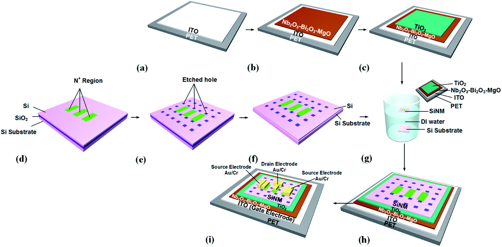 | ||
| Fig. 1 Process flow schematic of the flexible TFTs (drawn not to scale): (a) ITO deposited on the PET flexible substrate. (b) Nb2O3–Bi2O3–MgO deposited on the ITO/PET. (c) TiO2 deposited on the Nb2O3–Bi2O3–MgO/ITO/PET. (d) Source and drain active regions patterned and doped on SOI. (e) Hole array patterned and etched. (f) Buried oxide layer removed in HF. (g) The top SiNM released in DI water. (h) SiNM transferred onto the TiO2/Nb2O3–Bi2O3–MgO/ITO/PET substrate. (i) Source and drain electrodes formed by evaporating Cr/Au (30 nm/70 nm). | ||
Results and discussion
Fig. 2 shows the interface morphologies of Nb2O3–Bi2O3–MgO/TiO2 and the characteristics of Nb2O3–Bi2O3–MgO/TiO2 and Nb2O3–Bi2O3–MgO/TiO2/SiNM heterostructures. The scanning electron microscope (SEM) images of interface morphologies of Nb2O3–Bi2O3–MgO/TiO2 are shown in Fig. 2a and b, respectively. The AFM images of Nb2O3–Bi2O3–MgO and TiO2 layers are displayed in Fig. 2c and d. The calculated RMS of Nb2O3–Bi2O3–MgO and TiO2 is ∼4.13 nm and ∼2.45 nm, respectively. The AFM image and RMS values show consistent results to the SEM data, indicating that the surface of TiO2 is much smoother than that of Nb2O3–Bi2O3–MgO and has improved surface roughness to Nb2O3–Bi2O3–MgO layer, which contributes to reducing the carrier scattering center and improving the interface quality with SiNM.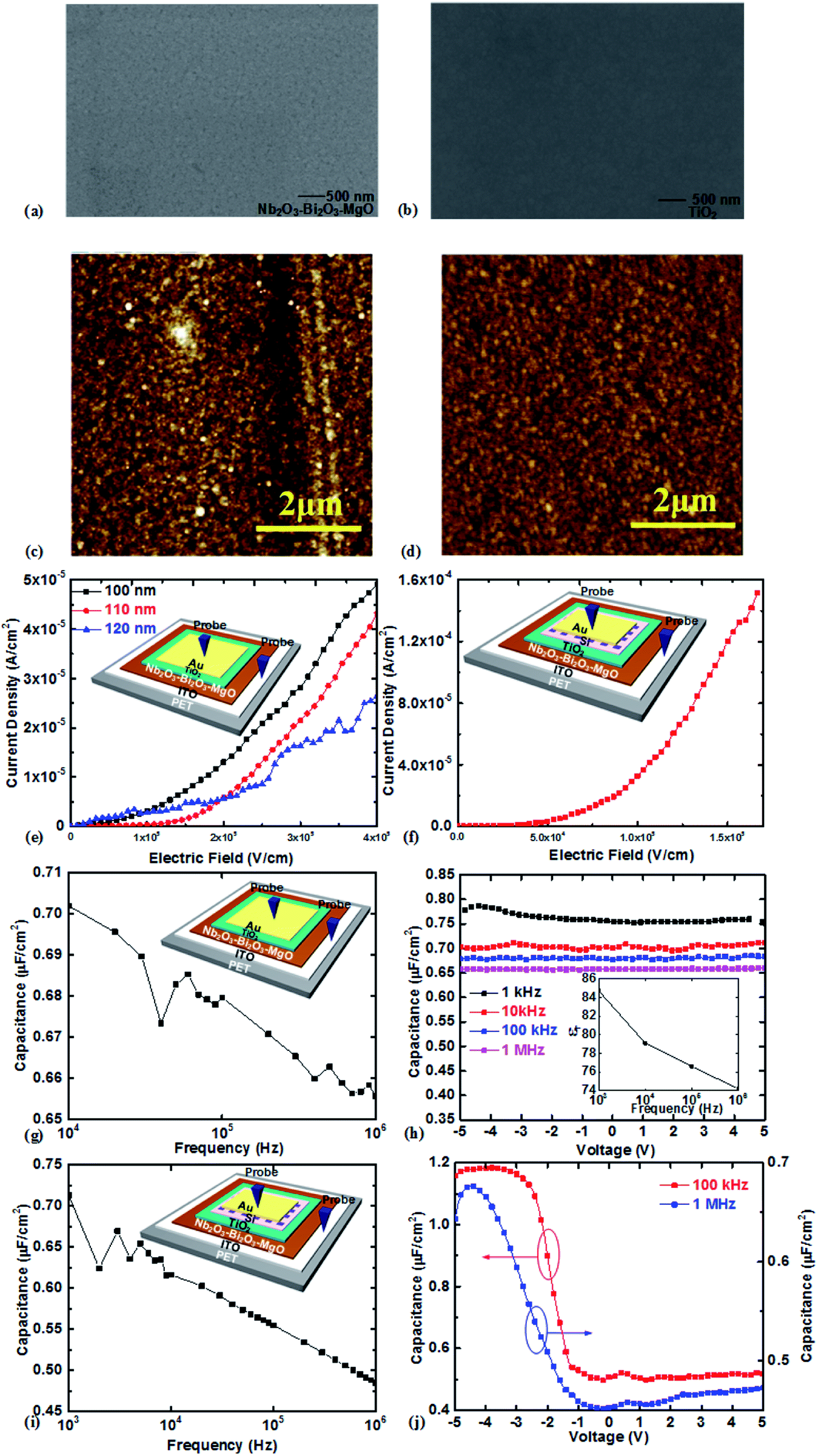 | ||
| Fig. 2 Surface morphologies and characteristics of Nb2O3–Bi2O3–MgO/TiO2 and Nb2O3–Bi2O3–MgO/TiO2/SiNM heterostructures: (a) SEM image of surface morphology of Nb2O3–Bi2O3–MgO. (b) SEM image of surface morphology of TiO2. (c) AFM image of surface morphology of Nb2O3–Bi2O3–MgO. (d) AFM image of surface morphology of TiO2. (e) Leakage current density of Nb2O3–Bi2O3–MgO/TiO2 heterostructure with different thickness. (f) Leakage current density of Nb2O3–Bi2O3–MgO/TiO2/SiNM heterostructure. (g) Frequency–capacitance characteristics of the Nb2O3–Bi2O3–MgO/TiO2 heterostructure. (h) Capacitance–voltage characteristics of the Nb2O3–Bi2O3–MgO/TiO2 heterostructure. (i) Frequency–capacitance characteristics of the Nb2O3–Bi2O3–MgO/TiO2/SiNM heterostructure. (j) Capacitance–voltage characteristics of the Nb2O3–Bi2O3–MgO/TiO2/SiNM heterostructure. | ||
Fig. 2e shows the leakage current density of Nb2O3–Bi2O3–MgO/TiO2 heterostructure with different thickness, indicating low leakage current density of the heterostructure. ∼100 nm dielectrics is chosen in this work. Fig. 2f shows the leakage current density of the Nb2O3–Bi2O3–MgO/TiO2/SiNM heterostructure, showing that the leakage current density is still very low even with the SiNM. The leakage current density of Nb2O3–Bi2O3–MgO/TiO2/SiNM is lightly higher than that of Nb2O3–Bi2O3–MgO/TiO2, because SiNM is lightly P-doped in which there are carrier drift with applied voltage.39 Frequency–capacitance and capacitance–voltage characteristic of the Nb2O3–Bi2O3–MgO/TiO2 heterostructure at 1 kHz, 10 kHz, 100 kHz and 1 MHz are shown in Fig. 2g and h, respectively. The capacitance slightly increases from ∼0.655 μF cm−2 to ∼0.75 μF cm−2 as frequency decreases from 1 MHz to 1 kHz, which indicates that the Nb2O3–Bi2O3–MgO/TiO2 heterostructure has low frequency sensitivity and the dielectric constant (εr) can be extracted from the following equation:
 | (1) |
Frequency–capacitance and capacitance–voltage characteristic of the Nb2O3–Bi2O3–MgO/TiO2/SiNM heterostructure at 100 kHz and 1 MHz are shown in Fig. 2i and j, respectively. The capacitance of the heterostructure can be calculated as follows:
 | (2) |
The capacitance–voltage curves consist of accumulation and inversion regions at high frequency of 100 kHz and 1 MHz. When a negative gate voltage is applied, the capacitance works in accumulation region and it equals to Cox. When the applied gate voltage increases, the inversion layer is formed at the Si/TiO2 interface and the capacitance of the Nb2O3–Bi2O3–MgO/TiO2/SiNM heterostructure is the series capacitances of Cox and the depletion capacitance in SiNM. Therefore, the capacitance of the heterostructure decreases and eventually keep stable as the gate voltage increases.
The optical image, microscope image and structure schematic of the flexible TFTs with Nb2O3–Bi2O3–MgO/TiO2/SiNM heterostructure fabricated on plastic substrates are shown in Fig. 3a–c, respectively. The transfer and I–V characteristics of TFT with channel width (W) and channel length (L) of 60 μm and 3 μm are shown in Fig. 3d and e, respectively, as an example, in which Ids is the drain current, gm is the transconductance, Vds is the drain voltage and Vgs is the gate voltage. The threshold voltage (Vth) extracted from Fig. 3d is ∼1.2 V, indicating that the flexible TFT has high drive capability. The saturation drain current of the flexible TFT is ∼28 μA with only ∼nA leakage current when the gate voltage is 2.5 V, and the current on/off ratio is over 104. The maximum transconductance of the flexible TFT reaches to ∼40 μS when gate voltage is 2.1 V. The subthreshold swing (SS) is calculated to be ∼0.2 V dec−1 by:
 | (3) |
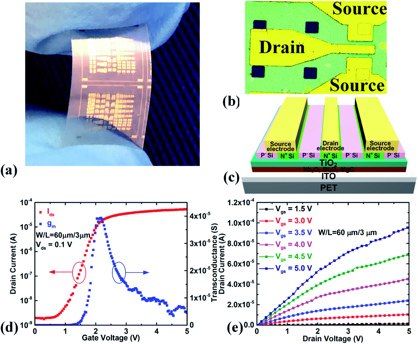 | ||
| Fig. 3 The optical image, microscope image, structure schematic and dc characteristics of the fabricated flexible TFTs: (a) the optical image of the flexible TFTs on a plastic substrate. (b) The microscope image of an example flexible TFT with double channels. (c) Structure schematic of the flexible TFT (drawn not to scale). (d) The transfer characteristics of an example flexible TFT with W/L = 60 μm/3 μm. (e) The I–V characteristics of the flexible TFT with W/L = 60 μm/3 μm. | ||
The interfacial trap density (Dit) can be calculated based on the SS value as follows:40
 | (4) |
Performance dependence of flexible TFTs on different dimensions are also investigated. Identical device structure is employed for the performance comparison.
Dependence on L
Fig. 4a and b show the transfer characteristics of flexible TFTs with different L (3 μm and 5 μm) and same W (60 μm) when Vds is 0.1 V, respectively. The threshold voltage of flexible TFT with W/L = 60 μm/3 μm is ∼1.2 V, which is slightly lower than that of TFT with W/L = 60 μm/5 μm (∼1.3 V). This is because that when the depletion generated by applying gate voltage is partially overlapped with the source and drain depletion, the inversion layer charge in the Si and dielectric interface decreases, causing the threshold voltage to slightly decrease.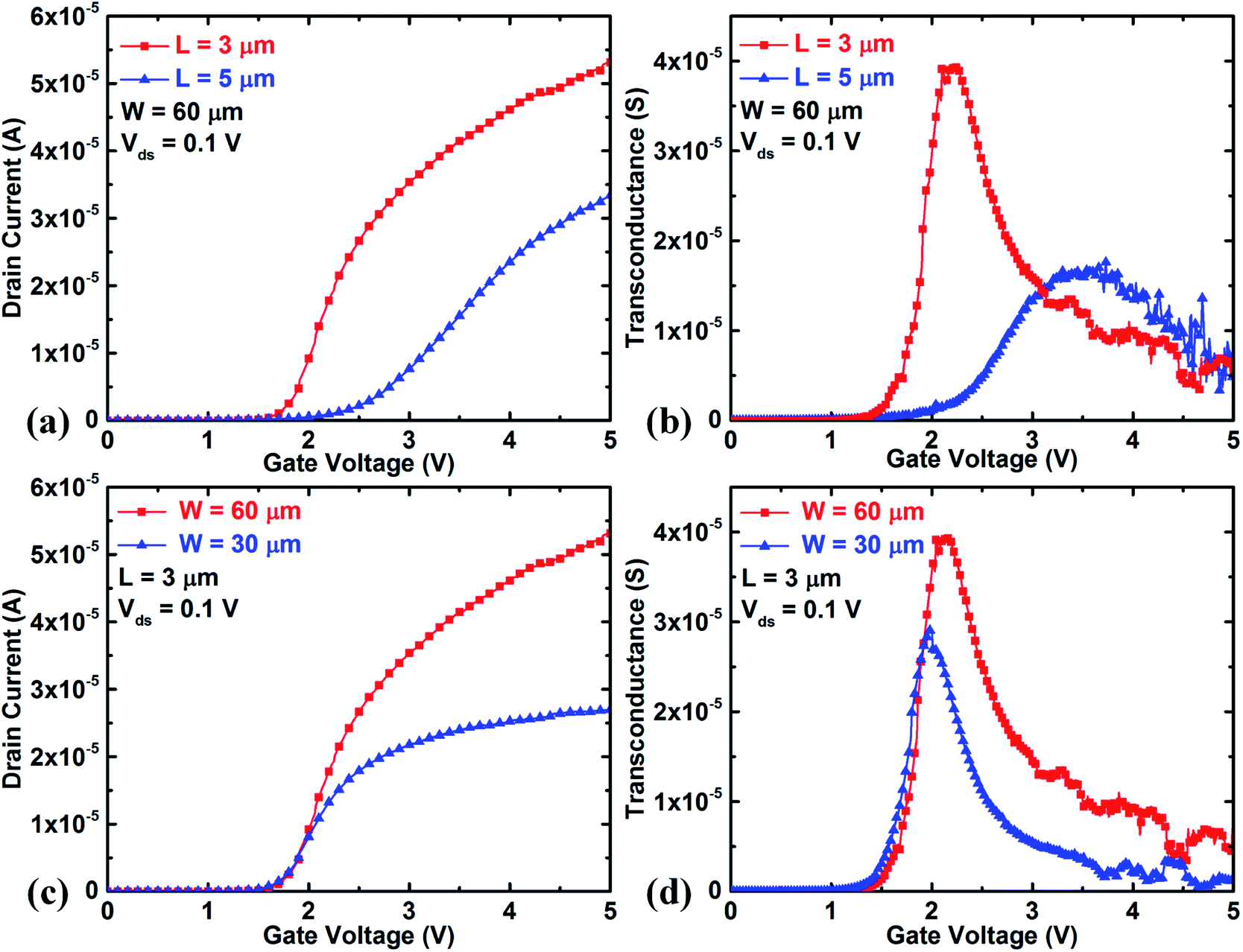 | ||
| Fig. 4 The performance dependence of flexible TFTs on different dimensions: (a) Ids and (b) transconductance comparisons of flexible TFTs with different L (3 μm and 5 μm). (c) Ids and (d) transconductance comparisons of flexible TFTs with different W (30 μm and 60 μm). | ||
The drain current is observed to be inversely proportional to L. Quantitatively, the saturation drain current of flexible TFT of L = 3 μm (∼53 μA) is ∼1.6 times of that of flexible TFT of L = 5 μm (∼33 μA), which is good agreement with theory calculation:
 | (5) |
 | (6) |
The transconductance of flexible TFTs is extracted from the following equation:
 | (7) |
It is also consistent with the experiment results and the highest transconductance reaches to ∼40 μS when the applied gate voltage is ∼2.1 V.
Dependence on W
Fig. 4c and d show the transfer characteristics of flexible TFTs with different W (30 μm and 60 μm) and same L (3 μm) when Vds is 0.1 V, respectively. The drain current is proportional to W.The saturation drain current of flexible TFT of W = 60 μm (∼53 μA) is 1.96 times of that of flexible TFT of W = 30 μm (∼27 μA), which is also in good agreement with the theory calculation. The results show that the fabricated flexible TFTs with Nb2O3–Bi2O3–MgO/TiO2/SiNM heterostructure have good performance consistency with different channel size.
Based on the experimental results, the advantages of the dielectric ceramics Nb2O3–Bi2O3–MgO/TiO2/SiNM heterostructure for flexible single-crystalline Si TFTs are analyzed and discussed as follows:
(1) The dielectric constant of the Nb2O3–Bi2O3–MgO/TiO2 dielectrics is extracted to be ∼76.6 (Fig. 2). The number is lower than the dielectric constant of Nb2O3–Bi2O3–MgO and higher than that of TiO2. Nevertheless, the dielectric constant of the heterostructure is much higher than those of SiO, SiOx or most low-temperature processed dielectrics, thus demonstrating that the heterostructure can be used as high-k gate dielectric material for high performance flexible devices.
(2) The SEM images and AFM images show that the surface of TiO2 is much smoother than that of Nb2O3–Bi2O3–MgO (Fig. 2) and the Dit of Si and dielectric (∼1012 eV−1 cm−2) is relatively low, which indicates that inserting TiO2 between SiNM and Nb2O3–Bi2O3–MgO can improve the interface quality. Additionally, the leakage current of Nb2O3–Bi2O3–MgO/TiO2/SiNM heterostructure is lower than that of TiO2/SiNM heterostructure. The reason for this is that dielectric ceramics layer Nb2O3–Bi2O3–MgO increases the conduction band offset between SiNM and TiO2, which can be explained from Fig. 5.
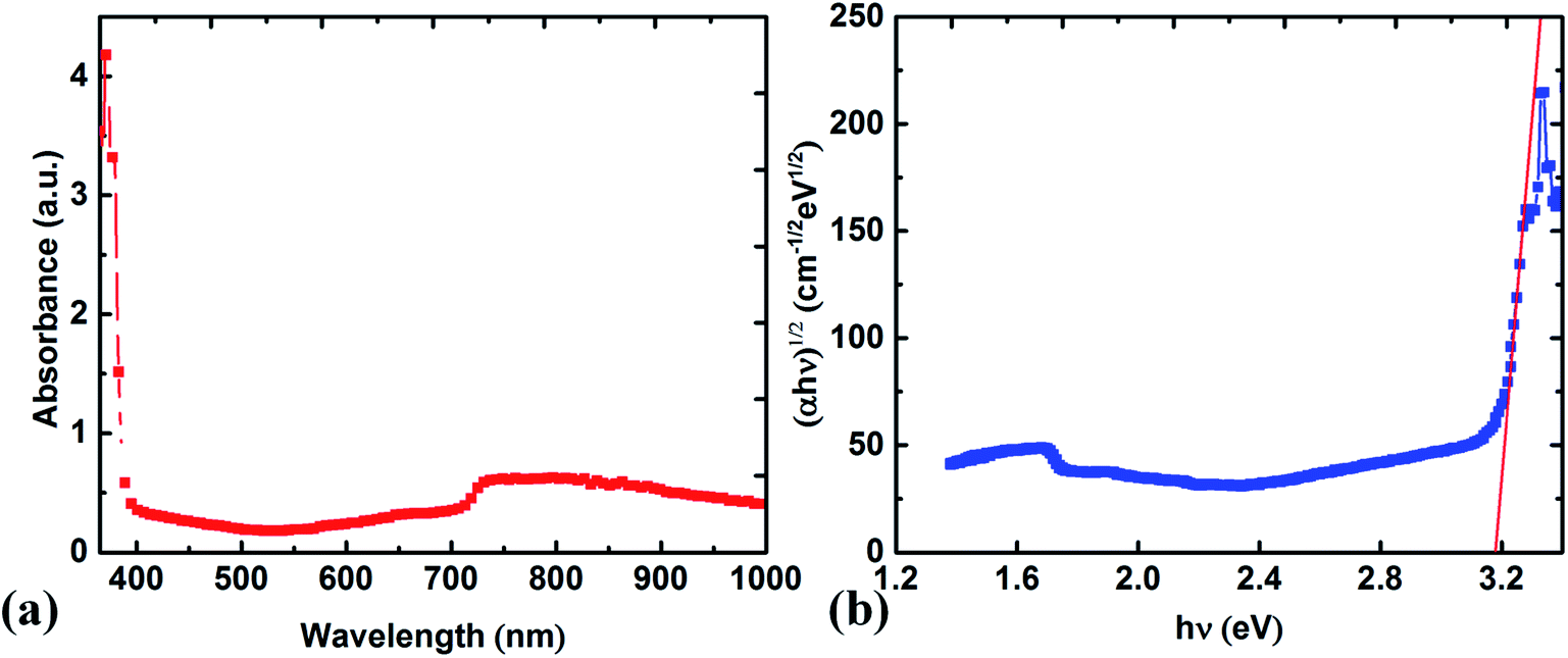 | ||
| Fig. 5 The spectra and band gap of Nb2O3–Bi2O3–MgO/TiO2 heterostructure: (a) the absorption spectra of the Nb2O3–Bi2O3–MgO/TiO2 heterostructure with wavelength from 365 nm to 1000 nm. (b) The extracted band gap of the Nb2O3–Bi2O3–MgO/TiO2 heterostructure. | ||
Fig. 5a shows the absorbance spectra of the Nb2O3–Bi2O3–MgO/TiO2 heterostructure with wavelength from 365 nm to 1000 nm. Based on the absorbance (Abs), the optical absorption coefficient (α) for the heterostructure can be calculated as follows:41
| α = 2.303(Abs/tox) | (8) |
The band gap of the Nb2O3–Bi2O3–MgO/TiO2 heterostructure can be extracted by the following equation42 as shown in the Fig. 5b:
| αhν = B(hν − Eg)2 | (9) |
Mechanical bending tests have been conducted for the fabricated flexible TFTs. The drain currents of the flexible TFTs are measured by attaching the devices onto molds with various curvature radii (from ∼77.5 mm to ∼28.5 mm). The flexible single-crystalline Si TFTs with Nb2O3–Bi2O3–MgO/TiO2/SiNM heterostructure on plastic substrates show slight performance variations, indicating good performance stability under mechanical bending conditions.
Conclusions
High performance flexible thin-film transistors (TFTs) with dielectric ceramics/TiO2/single-crystalline silicon nanomembrane (SiNM) heterostructure is designed and fabricated in this paper. Both the dielectric ceramics (Nb2O3–Bi2O3–MgO) and TiO2 are deposited by radio frequency (RF) magnetron sputtering at room temperature and the single-crystalline SiNM is transferred and attached to the dielectric ceramics/TiO2 layers to form the heterostructure. The experimental results demonstrate that the Nb2O3–Bi2O3–MgO/TiO2 heterostructure has high dielectric constant (∼76.6) and wider band gap than TiO2, which increases the conduction band offset between Si and TiO2, lowering the leakage current. The TiO2/single crystalline SiNM structure has relatively low interface trap density. Flexible TFTs fabricated with the Nb2O3–Bi2O3–MgO/TiO2/SiNM heterostructure on plastic substrates show a current on/off ratio over 104, threshold voltage of ∼1.2 V, subthreshold swing (SS) as low as ∼0.2 V dec−1, interface trap density of ∼1012 eV−1 cm−2 and good performance stability under mechanical bending conditions. The results indicate that the dielectric ceramics/TiO2/SiNM heterostructure has great potential for high performance TFTs.Conflicts of interest
There are no conflicts to declare.Acknowledgements
This work was supported by the National Natural Science Foundation of China (61871285), and by Tianjin Natural Science Foundation (18JCYBJC15900).References
- S. Park, S. W. Heo, W. Lee, D. Inoue, Z. Jiang, K. Yu, H. Jinno, D. Hashizume, M. Sekino, T. Yokota, K. Fukuda, K. Tajima and T. Someya, Nature, 2018, 561, 516–521 CrossRef CAS.
- W. Gao, S. Emaminejad, H. Y. Y. Nyein, S. Challa, K. V. Chen, A. Peck, H. M. Fahad, H. Ota, H. Shiraki, D. Kiriya, D. H. Lien, G. A. Brooks, R. W. Davis and A. Javey, Nature, 2016, 529, 509–514 CrossRef CAS.
- Y. Kim, A. Chortos, W. T. Xu, Y. X. Liu, J. Y. Oh, D. Son, J. Kang, A. M. Foudeh, C. X. Zhu, Y. Lee, S. M. Niu, J. Liu, R. Pfattner, Z. N. Bao and T. W. Lee, Science, 2018, 360, 998–1003 CrossRef CAS.
- B. C. K. Tee, A. Chortos, A. Berdnt, A. K. Nguyen, A. Tom, A. McGuire, Z. L. C. Liu, K. Tien, W. G. Bae, H. L. Wang, P. Mei, H. H. Chou, B. X. Cui, K. Deisseroth, T. N. Ng and Z. N. Bao, Science, 2015, 350, 313–316 CrossRef CAS.
- Y. C. Liu, Y. X. Zhang, Z. Yang, H. C. Ye, J. S. Feng, Z. Xu, X. Zhang, R. Munir, J. Liu, P. Zuo, Q. X. Li, M. X. Hu, L. N. Meng, K. Wang, D. M. Smilgies, G. T. Zhao, H. Xu, Z. P. Yang, A. Amassian, J. W. Li, K. Zhao and S. Z. Liu, Nat. Commun., 2018, 9, 5302 CrossRef.
- H. H. Chou, A. Nguyen, A. Chortos, J. W. F. To, C. Lu, J. G. Mei, T. Kurosawa, W. G. Bae, J. B. H. Tok and Z. A. Bao, Nat. Commun., 2015, 6, 8011 CrossRef CAS.
- G. X. Qin, H. C. Yuan, G. K. Celler, W. D. Zhou, J. G. Ma and Z. Q. Ma, Microelectron. J., 2011, 42, 509–514 CrossRef CAS.
- M. J. Dang, H. C. Yuan, Z. Q. Ma, J. G. Ma and G. X. Qin, Appl. Phys. Lett., 2017, 110, 253104 CrossRef.
- E. M. Song, Q. L. Guo, G. S. Huang, B. Jia and Y. F. Mei, ACS Appl. Mater. Interfaces, 2017, 9, 12171–12175 CrossRef CAS.
- G. X. Qin, H. C. Yuan, G. K. Celler, J. G. Ma and Z. G. Ma, Microelectron. Eng., 2012, 95, 21–25 CrossRef CAS.
- S. W. Hwang, H. Tao, D. H. Kim, H. Y. Cheng, J. K. Song, E. Rill, M. A. Brenckle, B. Panilaitis, S. M. Won, Y. S. Kim, Y. M. Song, K. J. Yu, A. Ameen, R. Li, Y. W. Su, M. M. Yang, D. L. Kaplan, M. R. Zakin, M. J. Slepian, Y. G. Huang, F. G. Omenetto and J. A. Rogers, Science, 2012, 337, 1640–1644 CrossRef CAS.
- S. W. Hwang, X. Huang, J. H. Seo, J. K. Song, S. Kim, S. Hage-Ali, H. J. Chung, H. Tao, F. G. Omenetto, Z. Q. Ma and J. A. Rogers, Adv. Mater., 2013, 25, 3526–3531 CrossRef CAS.
- S. W. Hwang, G. Park, H. Cheng, J. K. Song, S. K. Kang, L. Yin, J. H. Kim, F. G. Omenetto, Y. G. Huang, K. M. Lee and J. A. Rogers, Adv. Mater., 2014, 26, 1992–2000 CrossRef CAS.
- S. W. Hwang, J. K. Song, X. Huang, H. Y. Cheng, S. K. Kang, B. H. Kim, J. H. Kim, S. Yu, Y. G. Huang and J. A. Rogers, Adv. Mater., 2014, 26, 3905–3911 CrossRef CAS.
- S. W. Hwang, G. Park, C. Edwards, E. A. Corbin, S. K. Kang, H. Y. Cheng, J. K. Song, J. H. Kim, S. Yu, J. Ng, J. E. Lee, J. Kim, C. Yee, B. Bhaduri, Y. Su, F. G. Omennetto, Y. G. Huang, R. Bashir, L. Goddard, G. Popescu, K. M. Lee and J. A. Rogers, ACS Nano, 2014, 8, 5843–5851 CrossRef CAS.
- H. J. Yang, D. Y. Zhao, S. Chuwongin, J. H. Seo, W. Q. Yang, Y. C. Shuai, J. Berggren, M. Hammar, Z. Q. Ma and W. D. Zhou, Nat. Photonics, 2012, 6, 615–620 CrossRef.
- E. M. Song, H. Fang, X. Jin, J. N. Zhao, C. S. Jiang, K. J. Yu, Y. D. Zhong, D. Xu, J. H. Li, G. H. Fang, H. N. Du, J. Z. Zhang, J. M. Park, Y. G. Huang, M. A. Alam, Y. F. Mei and J. A. Rogers, Adv. Electron. Mater., 2017, 3, 1700077 CrossRef.
- A. Liu, H. H. Zhu, W. T. Park, S. J. Kang, Y. Xu, M. G. Kim and Y. Y. Noh, Adv. Mater., 2018, 30, 1802379 CrossRef.
- J. Q. Song, C. Y. Han and P. T. Lai, IEEE Trans. Electron Devices, 2016, 63, 1928–1933 CAS.
- H. J. Kwon, J. Jang and C. P. Grigoropoulos, ACS Appl. Mater. Interfaces, 2016, 8, 9314–9318 CrossRef CAS.
- P. F. Ma, J. M. Sun, G. D. Liang, Y. P. Li, Q. Xin, Y. X. Li and A. M. Song, Appl. Phys. Lett., 2018, 113, 063501 CrossRef.
- G. He, X. S. Chen and Z. Q. Sun, Surf. Sci. Rep., 2013, 68, 68–107 CrossRef CAS.
- G. He, J. W. Liu, H. S. Chen, Y. M. Liu, Z. Q. Sun, X. S. Chen, M. Liu and L. D. Zhang, J. Mater. Chem. C, 2014, 2, 5299–5308 RSC.
- J. W. Zhang, G. He, L. Zhou, H. S. Chen, X. S. Chen, X. F. Chen, B. Deng, J. G. Lv and Z. Q. Sun, J. Alloy. Compd, 2014, 611, 253–259 CrossRef CAS.
- G. He, J. Gao, H. S. Chen, J. B. Cui, Z. Q. Sun and X. S. Chen, ACS Appl. Mater. Interfaces, 2014, 6, 22013–22025 CrossRef CAS.
- K. Kukli, M. Kemell, M. Vehkamaki, M. J. Heikkila, K. Mizohata, K. Kalam, M. Ritala, M. Leskela, I. Kundrata and K. Fronhlich, AIP Adv., 2017, 7, 025001 CrossRef.
- X. Wang, H. X. Liu, C. X. Fei, L. Zhao, S. P. Chen and S. L. Wang, AIP Adv., 2016, 6, 065224 CrossRef.
- J. W. Liu and Y. Koide, Sensors, 2018, 18, 813 CrossRef PubMed.
- L. L. Zheng, S. B. Qian, Y. H. Wang, W. J. Liu and S. J. Ding, IEEE J. Electron Devices Soc., 2016, 4, 347–352 CAS.
- S. Jiang, X. Yang, J. H. Zhang and X. F. Li, AIP Adv., 2018, 8, 085109 CrossRef.
- H. F. Pu, H. L. Li, Z. Yang, Q. F. Zhou, C. Y. Dong and Q. Zhang, ECS Solid State Lett., 2013, 2, N35–N38 CrossRef CAS.
- X. W. Ding, J. H. Zhang, J. Li, W. M. Shi, H. Zhang, X. Y. Jiang and Z. L. Zhang, Superlattices Microstruct., 2014, 69, 204–211 CrossRef CAS.
- J. Li, F. Zhou, H. P. Lin, W. Q. Zhu, J. H. Zhang, X. Y. Jiang and Z. L. Zhang, Curr. Appl. Phys., 2012, 12, 1288–1291 CrossRef.
- H. Zhang, Y. Zhang, X. Chen, C. Y. Li and X. W. Ding, Mol. Cryst. Liq. Cryst., 2017, 651, 228–234 CrossRef CAS.
- X. S. Rong, H. F. Chen, J. Rong, X. Y. Zhang, J. Wei, S. Liu, X. T. Zhou, J. C. Xu, F. X. Qiu and Z. R. Wu, Chem. Eng. J., 2019, 371, 286–293 CrossRef CAS.
- V. K. Ashith, G. K. Rao, R. Smitha and S. N. Moger, Ceram. Int., 2018, 44, 17623–17629 CrossRef.
- Y. Y. Lin, C. C. Hsu, M. H. Tseng, J. J. Shyue and F. Y. Tsai, ACS Appl. Mater. Interfaces, 2015, 7, 22610–22617 CrossRef CAS.
- N. D. Chinh, C. Kim and D. Kim, J. Alloys Compd., 2019, 778, 247–255 CrossRef CAS.
- G. X. Qin, Y. B. Zhang, K. B. Lan, L. X. Li, J. G. Ma and S. H. Yu, ACS Appl. Mater. Interfaces, 2018, 10, 12798–12806 CrossRef CAS.
- D. B. Ruan, P. T. Liu, Y. C. Chiu, P. Y. Kuo, M. C. Yu, K. Z. Kan, T. C. Chien, Y. H. Chen and S. M. Sze, Thin Solid Films, 2018, 660, 578–584 CrossRef CAS.
- M. C. Sekhar, N. N. K. Reddy, H. S. Akkera, B. P. Reddy, V. Rajendar, S. Uthanna and S. H. Park, J. Alloys Compd., 2017, 718, 104–111 CrossRef.
- M. Maimaiti, B. H. Zhao, M. Mamat, Y. Tuersun, A. Mijiti, Q. Wang and Y. F. Sun, Mater. Res. Express, 2019, 6, 086408 CrossRef CAS.
- V. M. Naik, D. Haddad, R. Naik, J. Benci and G. W. Auner, Mater. Res. Soc. Symp. Proc., 2003, 755, 413–418 Search PubMed.
- K. Kaur and C. V. Singh, Energy Procedia, 2012, 29, 291–299 CrossRef CAS.
- Y. F. Ju, M. H. Wang, Y. L. Wang, S. H. Wang and C. F. Fu, Adv. Condens. Matter Phys., 2013, 365475 Search PubMed.
| This journal is © The Royal Society of Chemistry 2019 |