
 Open Access Article
 This Open Access Article is licensed under a Creative Commons Attribution-Non Commercial 3.0 Unported Licence
Electronic properties of α-graphyne on hexagonal boron nitride and α-BNyne substrates†
Maoyun Di a,
Lin Fua,
Yong Wanga,
Kaiyu Zhanga,
Yongjie Xua,
Hongzhe Pan*b,
Youwei Dua and
Nujiang Tang*a
a,
Lin Fua,
Yong Wanga,
Kaiyu Zhanga,
Yongjie Xua,
Hongzhe Pan*b,
Youwei Dua and
Nujiang Tang*a
aNational Laboratory of Solid State Microstructures, Collaborative Innovation Center of Advanced Microstructures, Jiangsu Provincial Key Laboratory for Nanotechnology, Nanjing University, Nanjing 210093, China. E-mail: tangnujiang@nju.edu.cn
bSchool of Physics and Electronic Engineering, Linyi University, Linyi 276005, China. E-mail: panhongzhe@lyu.edu.cn
First published on 31st October 2019
Abstract
The upsurge in the research of α-graphyne (α-GY) has occurred due to the existence of a Dirac cone, whereas the absence of band gap impedes its semiconductor applications. Here, the electronic properties of α-GY on hexagonal boron nitride (h-BN) and α-BNyne (α-BNy) monolayers are investigated using first-principles calculations. Through engineering heterostructures, the band gap opening can be achieved and has different responses to the substrate and stacking sequence. Intriguingly, the band gap of α-GY/α-BNy with Ab1 stacking mode is up to 77.5 meV in the HSE06 functional, which is distinctly greater than KBT at room temperature. The characteristic Dirac band of α-GY is preserved on the α-BNy substrate, while it changes into a parabolic band on the h-BN substrate. Additionally, we also find that changing the interlayer distance is an alternative strategy to realize the tunable band gap. Our results show that by selecting a reasonable substrate, the linear band structure and thus the high carrier mobility as well as the distinct band gap opening could coexist in α-GY. These prominent properties are the key quantity for application of α-GY in nanoelectronic devices.
1. Introduction
Two-dimensional (2D) nanomaterials, in which the electrons are confined in two dimensions, have ignited widespread attention due to their outstanding properties and promising applications. The most representative one is graphene exfoliated from graphite in 2004,1 given that its unusual properties, such as extremely high carrier mobility,2 quantum Hall effect,3 and Klein paradox,4 are rooted in the linear band dispersion characteristic Dirac cone. Inspired by graphene, carbon allotropes and their analogues have attracted extensive interest. Typically, graphyne (GY), a unique 2D carbon allotrope consisting of sp2 and sp hybridized carbon atoms,5 is greatly different from graphene which is only comprised of sp2 hybridized carbon atoms. Especially, the presence of acetylenic groups in GY can induce versatile structural and electronic properties.6,7 According to their distinct arrangement and percentage, the most fundamental geometrical structures can be divided into α-GY, β-GY, γ-GY, and 6,6,12-GY, in which the symmetry of the first three is hexagonal while the last one is rectangular.6 They also hold different electronic properties: γ-GY is semiconductor; the other three systems are all semimetals with Dirac cone.7 Notably, only α-GY is similar to graphene in both geometrical structure and electronic properties.7,8 It also possesses two equivalent Dirac cones at high symmetry points, K and K′ in the first Brillouin zone (BZ), rendering the excitations as massless Dirac fermions.8 Unfortunately, the zero-band-gap character restricts the semiconductor applications in constructing electronic devices. Therefore, it is of great significance to manipulate the band structure of α-GY.Some efforts have been made to manipulate the band structure of α-GY, such as tailoring,9,10 substitutional doping,11 chemical absorbing,12 applying the strain,13,14 and engineering heterostructure,15,16 etc. Notably, unlike other means that the carrier mobility would reduce more or less, engineering heterostructure can maintain the structural integrity and the novel properties of materials. Moreover, this means has been extensively applied in previous researches, such as graphene/MoS2,17 graphene/h-BN,18,19 graphyne/MSe2,20 and phosphorene/graphene,21 and so forth. However, the specific explanation for modulating the electronic properties of α-GY-based heterostructures is still scarce in previous researches.16 Therefore, we constructed the heterostructures of α-GY to manipulate its band structure, and provided a proposed mechanism.
Generally, for seeking an appropriate substrate, breaking the inversion symmetry plays a crucial role. It has been reported that (i) h-BN gets rid of dangling bonds and possess the large bandgap;22,23 (ii) the disparity of boron and nitrogen sublattices provides a drive to break inversion symmetry for h-BN and α-BNy; (iii) the lattice mismatch is quite small between h-BN or α-BNy and α-GY. Therefore, it is reasonable that h-BN and α-BNy can serve as ideal substrates for α-GY.
In this work, we investigated the electronic properties of α-GY/h-BN and α-GY/α-BNy based on the first-principles calculations. Our results indicate that the band gap is dependent on the substrate and stacking sequence. Particularly, for Ab1 stacking mode of α-GY/α-BNy, the band gap is up to 77.5 meV in the HSE06 functional, while the distinct gap larger than KBT at room temperature combined with the linear band dispersion indicates its potential applications in nanoelectronic devices. Furthermore, changing the interlayer distance provides a path for further manipulating the band gap.
2. Computational methods
All calculations were based on density functional theory (DFT) with projector augmented wave (PAW)24 method in the VASP package. The exchange-correlation potential was carried out using generalized gradient approximation (GGA) with the Perdew–Burke–Ernzerhof (PBE).25 The kinetic energy cutoff 600 eV was adopted for plane wave functions. The vacuum region was set to be larger than 15 Å along the direction perpendicular to the heterostructures in all of the simulations, to eliminate the interaction resulting from the periodicity of the lattice structure. A 7 × 9 × 1 k-point sampling generated by the Monkhorst–Pack grids26 in the BZ was applied for α-GY/h-BN while 13 × 13 × 1 k-point for α-GY/α-BNy. The geometries were allowed to relax fully until the forces on each atomic were below 0.02 eV Å−1. Since the dispersive force is exclusive in DFT calculations, DFT-D3 (ref. 27) was employed to describe van der Waals (vdW) interaction. In view of the fact that the PBE method usually underestimates the energy gap of semiconductor materials, the Heyd–Scuseria–Ernzerhof (HSE06) screened hybrid functional28 was also performed to further calculate the electronic properties. To elucidate the energetic stability, the binding energies were also calculated as follows:| Eb = (Eh − Em1 − Em2)/n | (1) |
3. Results and discussion
To reduce lattice mismatch, the rectangular unit cell of α-GY and h-BN was chosen during constructing the α-GY/h-BN, as shown in Fig. 1(a and b). Specifically, the rectangular unit cell of (3 × 1) α-GY sited on a rectangular unit cell of (5 × 5) h-BN substrate contains 148 atoms and could successfully match with the lattice mismatch 3.78%, which is acceptable in a theoretical investigation. The lattice mismatch more than 4% for graphene on Cu (111) surface has been researched in previous work.29 Moreover, moiré patterns of graphene disposed on Ir (111) with the lattice mismatch ∼10% were presented using scanning tunneling microscopy.30 As shown in Fig. 1(c), the lattice constant of the relaxed (1 × 1) α-BNy with the primitive cell, a = 7.11 Å, is quite close to that of (1 × 1) α-GY, and the comparable value with the previous study demonstrates the feasibility of our calculations.23 The lattice mismatch is subject to only 2%. Six emblematic configurations were considered respectively for two kinds of heterostructures. The detailed structural properties of these configurations were listed as Tables S1 and S2 in ESI.† It can be seen that the lattice constants of the most stable structure are a = 20.91 Å, b = 12.07 Å for α-GY/h-BN and a = b = 6.97 Å for α-GY/α-BNy, respectively corresponding to the minimum binding energies of −121.64 and −66.37 meV per atom. The negative binding energies reveal the heterostructures are more stable than the corresponding monolayers.31,32 In the following content, the most stable heterostructures will be clarified. | ||
| Fig. 1 The supercell of (a) α-GY, (b) h-BN, and (c) α-BNy. The green and purple dashed lines delineate primitive cell and rectangular unit cell, respectively. Top and side views of (d) α-GY/h-BN and (e) α-GY/α-BNy. | ||
The optimal schematic configurations were represented in Fig. 1(d and e). As shown in Fig. 1(d), the prominent fluctuations in the top and bottom layers of α-GY/h-BN respectively are of 1.47 and 3.16 Å, which may originate from lattice mismatch.20 To obtain the most stable heterostructure, the lattice constant of h-BN is compressed by 3.75%, which brings distinct interlayer interaction in different positions. Nevertheless, there are barely vital wrinkles (<0.35 Å) in two monolayers of α-GY/α-BNy (Fig. 1(e)). Such a magnitude of fluctuation has been found in B3CN4/BN, and it could keep the planar atom framework.33 Given the loose arrangements of the atoms between α-GY and h-BN monolayers, it is difficult to construct various stacking modes. However, the structural similarity between α-GY and α-BNy gives rise to nearly perfect atomic matching in α-GY/α-BNy and, thus the different stacking modes should be considered. Due to the difference of sublattices between α-GY and α-BNy, the atoms were marked as Fig. S1 in ESI.† Specifically, six different stacking modes, AA1, Ab1, Aa1, AB1, ab1, and aa1, were constructed similar to bilayer α-GY,34 and labeled as C–B condition. Obviously, exchanging the position of boron and nitrogen, the other six stacking modes, AA2, Ab2, Aa2, AB2, ab2, and aa2, were reconstructed, correspondingly labeled as C–N condition. It is found that AA1 is identical to AA2 because of the periodicity of the lattice structure, so they are collectively called AA stacking mode. Therefore, we considered eleven distinct stacking modes for α-GY/α-BNy (see Fig. S1 in ESI†). After full relaxation, all stacking modes have no meaningful bend, and the most stable stacking modes are Ab1 and Ab2 for two cases. Furthermore, the binding energies of the different stacking modes show a very small difference, demonstrating that they may coexist. Thus, the different stacking modes will be considered in the following.
The interlayer distance of two heterostructures presents a great difference with the corresponding values of 1.69 (see Table S1 in ESI†) and 2.87–3.35 Å (Table 1), respectively. This implies that it relies not only on the substrate material but also on the stacking mode. Moreover, the interlayer distance increases roughly with the increase of overlapping atoms in these stacking modes, and the slight change suggests the presence of a substantial repulsive Pauli interaction.35 In addition, the value of the interlayer distance is more than the sum of the covalent atom radius, beyond the bonding range. Hence, there exists weak interlayer interaction, such as vdW interaction.
| C–B | AA1 | Ab1 | Aa1 | AB1 | ab1 | aa1 |
|---|---|---|---|---|---|---|
| Binding energy (meV per atom) | −66.36 | −69.75 | −69.60 | −69.56 | −69.16 | −69.10 |
| Interlayer distance (Å) | 3.35 | 3.34 | 2.98 | 2.91 | 2.98 | 2.91 |
| C–N | AA2 | Ab2 | Aa2 | AB2 | ab2 | aa2 |
|---|---|---|---|---|---|---|
| Binding energy (meV per atom) | −66.36 | −70.01 | −69.35 | −69.54 | −69.10 | −69.16 |
| Interlayer distance (Å) | 3.35 | 3.20 | 3.05 | 2.87 | 2.91 | 2.94 |
The band structures were calculated for the isolated α-GY, h-BN, and α-BNy monolayer, as well as all heterostructures. For two unit cells of isolated α-GY monolayers, the valence and conduction bands touch in a single point around Fermi level (Fig. 2(a and d)), showing that α-GY is semimetal. Note that the K point of the isolated α-GY monolayer with the rectangular unit cell is folded into the Γ point because of the BZ folding. For the isolated h-BN and α-BNy monolayer, the wide gaps respectively arise with the values of 4.68 and 4.21 eV (Fig. 2(b and e)), indicating that both h-BN and α-BNy are insulators. These results are coincident with the results reported,7,23,36,37 which implies that the accuracy of our calculation.
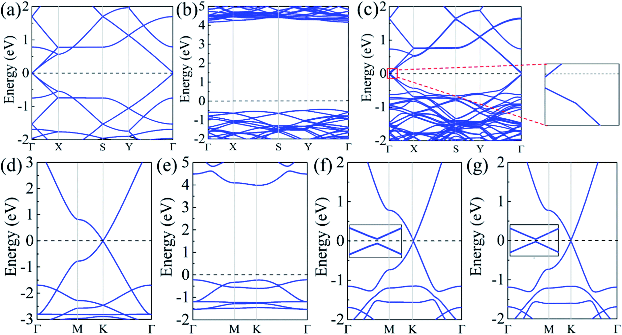 | ||
| Fig. 2 Band structures of (a) the isolated α-GY monolayer with the rectangular unit cell, (b) the isolated h-BN monolayer, (c) α-GY/h-BN, (d) the isolated α-GY monolayer with the primitive cell, (e) the isolated α-BNy monolayer, (f) Ab1 stacking mode of α-GY/α-BNy, and (g) Ab2 stacking mode of α-GY/α-BNy. The insets are band structures around the Fermi level. The horizontal dashed lines represent that the Fermi level is shifted to zero. | ||
With a view to the possibility of the practical applications, the most stable stacking modes, Ab1 and Ab2, were illuminated in detail for α-GY/α-BNy. The band structures of the heterostructures were shown in Fig. 2(c, f and g). It can be seen that the band structures seem to be a simple superimposed of each constituent apart from an apparent downward movement of the whole α-BNy. The trend of the corresponding band of α-GY is retained near Fermi level, while that of h-BN and α-BNy is far away from Fermi level. This is in accord with the weak interlayer interaction as mentioned above. Interestingly, the valence and conduction bands repulse each other, forming the significant band gaps of 10.6, 27.5, and 16.0 meV for α-GY/h-BN, Ab1-, and Ab2-stacking of α-GY/α-BNy (insets of Fig. 2(c, f and g)), respectively. It indicates that all these heterostructures realize the transformation from semimetal to semiconductor. The band gap opening shows the sublattice symmetry has been broken. Meanwhile, the characteristic Dirac band around K point and thus its high carrier mobility of α-GY is retained on α-BNy substrate. In contrast, its band structure changes into the parabolic around Γ point on h-BN substrate. In view of the meaningfulness of the tunable band gap for the applications in nanoelectronics and nanophotonics, we calculated the band gaps as a function of the interlayer distance (shown in Fig. 3). It is obvious that the band gap gradually decreases with the increasing interlayer distance for two heterostructures, which is similar to graphene on hexagonal boron nitride.29 The distinct variation indicates that changing the interlayer distance can pave a path for manipulating the band gap.
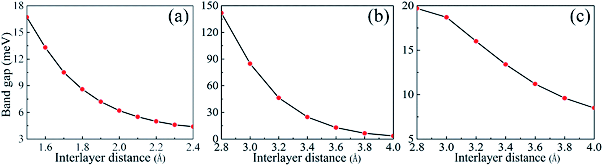 | ||
| Fig. 3 The band gaps as a function of the interlayer distance of (a) α-GY/h-BN, (b) Ab1 stacking mode of α-GY/α-BNy, and (c) Ab2 stacking mode of α-GY/α-BNy. | ||
Considering the fact that the PBE method generally underestimates the energy gap, we adopted the hybrid functional calculations based on the HSE06 functional to calculate the gap values. Due to the high computational cost and long computational time, this method was just carried out to correct the band gap of α-GY on α-BNy substrate, whereas the PBE method was used to forecast the trends of the band structures of α-GY on h-BN substrate on account of the larger geometric construction. It is found that the energy gaps respectively increase to 77.5 and 20.9 meV for Ab1-and Ab2-stacking modes, both of which are larger than the corresponding values of 27.5 and 16.0 meV in PBE method. Note that the gap of the Ab1 stacking mode is well above KBT at room temperature and thus could resist the thermal fluctuations of the excitations,38 while the linear band dispersion is still unchanged. The band gap opening of α-GY is larger and more significant for Ab1 stacking mode, comparing to that of Ab stacked bilayer α-GY with 29 meV in previous research.34 Clearly, the significant great band gap combined with the high carrier mobility is favorable to its potential applications in nanoelectronic devices.
As widely applied in previous studies,17,34 the band structure can be approximatively comprehended by tight-binding approximation and the electronic dispersion relation can be approximately represented via
| E(k) = ±(Δ2/4+(ħvFk)2)1/2 | (2) |
Projected density of states (PDOS) offers an effective way to comprehend the nature of the band structure. As shown in Fig. 4, the conduction band minimum (CBM) and valence band maximum (VBM) are contributed by the 2pz orbitals of C atoms, whereas the 2px+y of C atoms, B and N atoms are barely contributions for two heterostructures. In contrast, the valence bands mainly root in the N atoms, while the conduction bands are mainly due to B atoms and 2px+y orbitals of C atoms. To further analyze the band structure, the band-decomposed charge density of CBM and VBM at Γ point for h-BN substrate and K point for α-BNy substrate was plotted in insets of Fig. 4. It is clear that both the CBM and the VBM wave functions locate in the α-GY monolayer. These results coincide with the conclusions mentioned above, which is revealed by the electronic band spectrum.
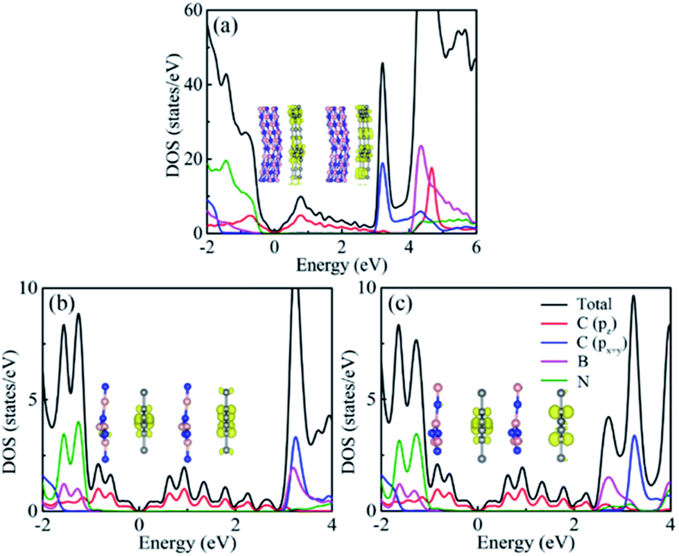 | ||
| Fig. 4 Total DOS and PDOS of (a) α-GY/h-BN, (b) Ab1 stacking mode of α-GY/α-BNy, and (c) Ab2 stacking mode of α-GY/α-BNy. The insets represent the corresponding band-decomposed charge densities for the VBM (left) and CBM (right). The blue, pink, and gray balls are N, B, and C atoms, respectively. | ||
Besides, it is found that different substrates also have some unique phenomena. In the case of α-GY/h-BN, the bands are split due to the interlayer coupling. In addition, the Fermi level shifts upwardly to the conduction band, showing slight n-type self-doping phenomenon. Specifically, there exist charge carries in the neutral state, which renders an advantage for its application in nanoelectronic devices. Utilizing the Bader charge analysis43,44 (see Table S3 in ESI†), the slight negative electron resides in the α-GY layer, which leads to the n-type self-doping phenomenon and verifies the weak interlayer interaction. For different stacking modes of α-GY/α-BNy, their band structures represent linear dispersion relation except that AA stacking mode shows the parabolic band structure (see Fig. S2 and S3 in ESI†). As reported that the asymmetric quantum confinement effect induced by the disparate coupling strengths in the different stacking modes could be the cause of discrepant electronic dispersions.45 Among all these modes, the band gap reaches 64 meV for AA stacking mode, whereas it is only 2.9 and 3.9 meV for AB1 and AB2 stacking modes, respectively. It can be concluded that the stacking method plays a vital role in the band gap. If the stability of AA stacking mode can be confirmed, this is beneficial to its electronic applications.
To understand the mechanism of the charge transfer, plane-averaged electron density difference along the direction perpendicular to the heterostructures is investigated. It can be gained by
| Δρ = ρh − ρm1 − ρm2 | (3) |
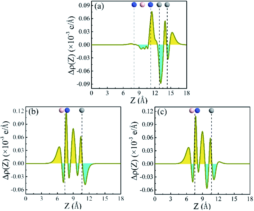 | ||
| Fig. 5 Plane-average electron density difference plot of the heterostructures along the Z axis. (a) α-GY/h-BN. (b) Ab1 stacking of α-GY/α-BNy. (c) Ab2 stacking of α-GY/α-BNy. The vertical dashed lines indicate the position of the C atoms in α-GY monolayer, and the B and N atoms in h-BN or α-BNy monolayer, respectively. The yellow and cyan areas represent electron accumulation and depletion, respectively. The blue, pink, and gray balls are N, B, and C atoms, respectively. | ||
4. Conclusions
In conclusion, using first-principle calculations based on DFT with the PAW method, we investigated the electronic properties of α-GY/h-BN and α-GY/α-BNy heterostructures. Owing to the negative binding energy and the acceptable lattice mismatch, the stability of the heterostructures were demonstrated. The results imply that Ab1- and Ab2-stacking modes are the most stable structures for α-GY sited on α-BNy substrate. Obvious band gaps have been respectively opened with 10.6, 27.5, and 16.0 meV for α-GY/h-BN, Ab1-, and Ab2-stacking mode of α-GY/α-BNy, the difference of which is contributed to the distinct arrangements of structures and electronegativities of elements in the heterostructures. It is found that the band gap of α-GY respectively increases to 77.5 and 20.9 meV for Ab1- and Ab2-stacking mode of α-GY/α-BNy by utilizing the more accurate HSE06 functional calculations. Moreover, the characteristic Dirac band of α-GY is retained in α-GY/α-BNy, while changes into the parabolic band in α-GY/h-BN. Particularly, for Ab1 stacking mode of α-GY/α-BNy, the band gap significantly greater than KBT at room temperature and the linear band dispersion signify its potential applications in nanoelectronic devices. These results indicate that the electronic properties of α-GY are sensitive to the substrates and stacking orders. In addition, the band gap can be modulated by changing the interlayer distance, which is an alternative strategy in the applications. The variation of the band structure origins from the symmetry breaking in the two sublattices of α-GY, which is driven by the charge redistribution. Our results can offer a significant theoretical foundation for the potential applications of α-GY in nanoelectronic devices where the finite band gap and high carrier mobility are required.Conflicts of interest
There are no conflicts to declare.Acknowledgements
This work was financially supported by the State Key Program for Basic Research (Grant No. 2017YFA0206304), National Natural Science Foundation of China (Grant No. 51572122), and the Natural Science Foundation of Shandong Province (Grant No. ZR2019MA042). We are grateful to the High Performance Computing Center of Nanjing University for doing the numerical calculations in this paper on its blade cluster system. We are grateful to Prof. Sun Jian for his guidance on this work.References
- K. S. Novoselov, A. K. Geim, S. V. Morozov, D. Jiang, Y. Zhang, S. V. Dubonos, I. V. Grigorieva and A. A. Firsov, Science, 2004, 306, 666–669 CrossRef CAS.
- A. H. Castro Neto, F. Guinea, N. M. R. Peres, K. S. Novoselov and A. K. Geim, Rev. Mod. Phys., 2009, 81, 109–162 CrossRef CAS.
- Y. Zhang, Y. W. Tan, H. L. Stormer and P. Kim, Nature, 2005, 438, 201–204 CrossRef CAS PubMed.
- M. I. Katsnelson, K. S. Novoselov and A. K. Geim, Nat. Phys., 2006, 2, 620–625 Search PubMed.
- R. H. Baughman, H. Eckhardt and M. Kertesz, J. Chem. Phys., 1987, 87, 6687 CrossRef CAS.
- Q. Peng, A. K. Dearden, J. Crean, L. Han, S. Liu, X. Wen and S. De, Nanotechnol., Sci. Appl., 2014, 7, 1–29 CAS.
- D. Malko, C. Neiss, F. Vines and A. Gorling, Phys. Rev. Lett., 2012, 108, 086804 CrossRef.
- W. Wu, W. Guo and X. C. Zeng, Nanoscale, 2013, 5, 9264–9276 RSC.
- V. R. Coluci, S. F. Braga, S. B. Legoas, D. S. Galvão and R. H. Baughman, Phys. Rev. B: Condens. Matter Mater. Phys., 2003, 68, 035430 CrossRef.
- H. Jafarzadeh, M. R. Roknabadi, N. Shahtahmasebi and M. Behdani, Phys. E, 2015, 67, 54–58 CrossRef CAS.
- A. Ruiz-Puigdollers and P. Gamallo, Carbon, 2017, 114, 301–310 CrossRef CAS.
- R. Majidi, Can. J. Chem., 2016, 94, 229–233 CrossRef CAS.
- S. Behzad, J. Electron. Mater., 2018, 47, 5601–5606 CrossRef CAS.
- Z. Li, Z. Liu and Z. Liu, Nano Res., 2017, 10, 2005–2020 CrossRef CAS.
- Y. Ren, Y. Zhang, J. Yun and Z. Zhang, Mater. Res. Express, 2018, 6, 016309 CrossRef.
- S. Behzad, Eur. Phys. J. B, 2019, 92, 7 CrossRef.
- Y. Ma, Y. Dai, M. Guo, C. Niu and B. Huang, Nanoscale, 2011, 3, 3883–3887 RSC.
- N. Jain, F. Yang, R. B. Jacobs-Gedrim, X. Xu, M. P. Anantram and B. Yu, Carbon, 2018, 126, 17–22 CrossRef CAS.
- A. Ramasubramaniam, D. Naveh and E. Towe, Nano Lett., 2011, 11, 1070–1075 CrossRef CAS.
- Q. Sun, Y. Dai, Y. Ma, W. Wei and B. Huang, J. Phys. Chem. Lett., 2015, 6, 2694–2701 CrossRef CAS.
- Y. Cai, G. Zhang and Y. W. Zhang, J. Phys. Chem. C, 2015, 119, 13929–13936 CrossRef CAS.
- L. Liu, Y. P. Feng and Z. X. Shen, Phys. Rev. B: Condens. Matter Mater. Phys., 2003, 68, 104102 CrossRef.
- V. O. Özçelik and S. Ciraci, J. Phys. Chem. C, 2013, 117, 2175–2182 CrossRef.
- G. Kresse and D. Joubert, Phys. Rev. B: Condens. Matter Mater. Phys., 1999, 59, 1758–1775 CrossRef CAS.
- J. P. Perdew, K. Burke and M. Ernzerhof, Phys. Rev. Lett., 1996, 77, 3865–3868 CrossRef CAS.
- H. J. Monkhorst and J. D. Pack, Phys. Rev. B: Solid State, 1976, 13, 5188–5192 CrossRef.
- S. Grimme, J. Antony, S. Ehrlich and H. Krieg, J. Chem. Phys., 2010, 132, 154104 CrossRef.
- J. Heyd, G. E. Scuseria and M. Ernzerhof, J. Chem. Phys., 2003, 118, 8207–8215 CrossRef CAS.
- G. Giovannetti, P. A. Khomyakov, G. Brocks, P. J. Kelly and J. van den Brink, Phys. Rev. B: Condens. Matter Mater. Phys., 2007, 76, 073103 CrossRef.
- A. T. N'Diaye, S. Bleikamp, P. J. Feibelman and T. Michely, Phys. Rev. Lett., 2006, 97, 215501 CrossRef.
- J. Cui, S. Liang and J. Zhang, Phys. Chem. Chem. Phys., 2016, 18, 25388–25393 RSC.
- J. Yun, Y. Zhang, Y. Ren, M. Xu, J. Yan, W. Zhao and Z. Zhang, Phys. Chem. Chem. Phys., 2018, 20, 26934–26946 RSC.
- H. Pan, H. Zhang, Y. Sun, Y. Ding, J. Chen, Y. Du and N. Tang, Phys. Chem. Chem. Phys., 2017, 19, 14801–14810 RSC.
- O. Leenaerts, B. Partoens and F. M. Peeters, Appl. Phys. Lett., 2013, 103, 013105 CrossRef.
- J. Berashevich and T. Chakraborty, J. Phys. Chem. C, 2011, 115, 24666–24673 CrossRef CAS.
- M. Topsakal, E. Aktürk and S. Ciraci, Phys. Rev. B: Condens. Matter Mater. Phys., 2009, 79, 115442 CrossRef.
- Y. Zhang, J. Yun, K. Wang, X. Chen, Z. Yang, Z. Zhang, J. Yan and W. Zhao, Comput. Mater. Sci., 2017, 136, 12–19 CrossRef CAS.
- P. Leubner, L. Lunczer, C. Brune, H. Buhmann and L. W. Molenkamp, Phys. Rev. Lett., 2016, 117, 086403 CrossRef.
- J. B. Oostinga, H. B. Heersche, X. Liu, A. F. Morpurgo and L. M. Vandersypen, Nat. Mater., 2008, 7, 151–157 CrossRef CAS.
- Y. Fan, M. Zhao, Z. Wang, X. Zhang and H. Zhang, Appl. Phys. Lett., 2011, 98, 083103 CrossRef.
- N. Lu, H. Guo, Z. Zhuo, L. Wang, X. Wu and X. C. Zeng, Nanoscale, 2017, 9, 19131–19138 RSC.
- R. Quhe, J. Zheng, G. Luo, Q. Liu, R. Qin, J. Zhou, D. Yu, S. Nagase, W.-N. Mei, Z. Gao and J. Lu, NPG Asia Mater., 2012, 4, E6 CrossRef.
- G. Henkelman, A. Arnaldsson and H. Jónsson, Comput. Mater. Sci., 2006, 36, 354–360 CrossRef.
- E. Sanville, S. D. Kenny, R. Smith and G. Henkelman, J. Comput. Chem., 2007, 28, 899–908 CrossRef CAS.
- C. Li, J. Gao, Y. Zi, F. Wang, C. Niu, J.-H. Cho and Y. Jia, Carbon, 2018, 140, 164–170 CrossRef CAS.
Footnote |
| † Electronic supplementary information (ESI) available. See DOI: 10.1039/c9ra07869j |
| This journal is © The Royal Society of Chemistry 2019 |