
 Open Access Article
 This Open Access Article is licensed under a Creative Commons Attribution-Non Commercial 3.0 Unported Licence
High responsivity ultraviolet detector based on novel SnO2 nanoarrays†
Xinhua Pan *,
Tao Zhang,
Qiaoqi Lu,
Weihao Wang and
Zhizhen Ye
*,
Tao Zhang,
Qiaoqi Lu,
Weihao Wang and
Zhizhen Ye
State Key Laboratory of Silicon Materials, Cyrus Tang Center for Sensor Materials and Applications, School of Materials Science and Engineering, Zhejiang University, Hangzhou 310027, People's Republic of China. E-mail: panxinhua@zju.edu.cn
First published on 14th November 2019
Abstract
In this work, tin oxide (SnO2) nanoarrays (NAs) with a novel morphology were fabricated by a hydrothermal method. Each SnO2 nanorod (NR) consisted of a bunch of nearly ten primary NRs with a width of 4–7 nm. On this basis, gold (Au) nanoparticles (NPs) were used to induce the growth of smaller and more orderly SnO2 NAs. The prepared ultraviolet (UV) detectors based on SnO2 NAs have high responsivity and high external quantum efficiency (EQE) under 20 μW cm−2 UV light with only 1 V external bias voltage.
1. Introduction
As a new civil and military technology, ultraviolet (UV) detectors has been widely used in many fields, such as UV communication, forest fire prevention, pollution monitoring and biomedical diagnosis.1–4 Up to now, the research of UV detectors has gradually developed from vacuum diodes, photomultipliers and silicon photodiodes to the third generation of wide band gap semiconductor based UV detectors. With unique physical and chemical properties, nanostructured metal oxide semiconductors have been proposed for UV detectors with superior responsivity, high quantum efficiency, low-power consumption, and weak signal detection.3–6Tin oxide (SnO2), a direct band gap semiconductor with a wide band gap of 3.6–3.8 eV, shows strong exciton binding potential of 130 meV and transparency in visible spectral region.7 It is considered to be a candidate for visible blind photodetectors.8 Previous studies on nanostructured SnO2 mainly focused on morphology and structure. SnO2 nanospheres, nanorods (NRs), nanobelts, nanotubes and other morphologies have been controllably prepared and widely reported.9 However, progress in high-performance photodetectors based on nanostructured SnO2 is limited,10 compared with other wide band gap semiconductors such as zinc oxide (ZnO) and titanium oxide (TiO2). Until recent years, some reports on nanostructured SnO2 based UV detectors gradually appeared. However, it is studied that the devices constructed by pure nanostructured SnO2 exhibit poor performance in UV detection, due to the surface defects and trapping effect from oxygen molecules adsorbed on the surface of SnO2.11,12 J. M. Wu et al.13 synthesized SnO2 nanowires by gas–liquid–solid method at 900 °C, and fabricated UV detectors on Al substrates. The sensitivity of the devices under 365 nm UV irradiation was only 0.69. Therefore, many efforts have been devoted to improve the performance of SnO2 based photodetectors. Fabricating complex high-precision devices and utilizing heterojunctions are usually effective methods to improve device performance.13–19 J. Yan et al.14 constructed SnO2 nanowires UV detectors with a series of complex optical elements such as spatial light modulators and microscopes. The acquired detectors showed high sensitivity, responsivity and external quantum efficiency (EQE). C. L. Hsu et al.15 prepared Ga2O3/SnO2:Ga core–shell nanowires on sapphire substrates by gas–liquid–solid method at 1000 °C. Under 310 nm UV irradiation, the Ion/Ioff of Ga-doped devices is 1066.7, but the maximum quantum efficiency is only 0.362%. In addition, S. Abbas et al.16 reported a transparent photodetector governed by a SnO2/SnS2 heterojunction, but they had to introduce an In2O3 nanolayer in the SnO2/SnS2 heterojunction to reduce the dark current. Interestingly, Gan et al.12 reported a novel UV detector based on the kinked SnO2 nanowires, which shows better performance than the conventional straight SnO2 nanowire-based photodetectors both in photocurrent and photoresponse speed. The improvement is caused by the enhancement effect of the kinked structure in SnO2 nanowires to the local electric field, which benefits for the charge separation efficiency and the transmittal time of carriers. However, the exact mechanism of the formation of the kinked SnO2 nanowires is not clear yet.
Complex synthesis method and device structure may hinder the widespread application of nanostructured SnO2 based UV detectors. Accordingly, how to improve the comprehensive performance of SnO2 based detectors by a simple way is the main challenge for SnO2 nanostructured based UV detectors. In this work, we have successfully prepared SnO2 nanoarrays (NAs) with peculiar morphology and neat arrangement by a controllable and simple hydrothermal method, and fabricated devices based on SnO2 NAs with high responsivity. Furthermore, we introduced gold (Au) nanoparticles in order to obtain more compact SnO2–Au NAs, and the devices exhibit better performance than pure SnO2 NAs with the help of localized surface plasmon resonances (LSPR). In particularly, SnO2–Au NAs UV detectors work at low additional bias voltage and show high responsivity, external quantum efficiency and detectivity under weak power UV light (20 μW cm−2). More importantly, this work reveals that nanostructured SnO2 based UV detectors can be developed towards weak signal detection and low-power consumption.
2. Experimental section
2.1 Synthesis of SnO2 NAs
In this work, the SnO2 NAs were prepared by hydrothermal method.18 0.1234 g NaBr was dissolved in 3.6 ml deionized water, and 0.1043 g SnCl4·5H2O was dissolved in 24 ml acetic acid. Under continuous stirring, the two drops were added into 4 ml ethanol to obtain a yellowish liquid. Fluorine-doped tin oxide (FTO) substrates were ultrasonically cleaned in beakers containing acetone, ethanol and deionized water, respectively, and then blown dry with nitrogen. The conductive layer was upward and placed in a 50 ml Teflon-sealed autoclave. The yellowish solution was transferred into the Teflon-sealed autoclave and heated to 200 °C, maintained for 12 hours. When the hydrothermal reaction was completed and the autoclave was cooled to room temperature naturally, samples were taken out with tweezers, washed alternately with deionized water and ethanol, then cleaned by ultrasound in ethanol, and finally dried at 60 °C for 12 hours.Electron beam evaporation were used to grow 50 nm thick Au NPs on the cleaned FTO conductive layer as the substrate and repeated the above steps to obtain Au-induced SnO2 NAs. For convenience, Au-induced SnO2 NAs were named as SnO2–Au NAs. UV detectors based on SnO2 NAs were abbreviated by using electron beam evaporation to coat aluminum (Al) on NAs as electrodes.
2.2 Characterization
The surface morphology and crystal structure of the samples were characterized by field-emission scanning electron microscopy (FE-SEM, Hitachi S-4800) and transmission electron microscopy (TEM, PhilipsTecnai F20). The crystallinity of SnO2 NAs was analyzed by X-ray diffraction (XRD) with a Cu Kα radiation source (λ = 1.54056 Å). The light reflection of the samples was characterized by ultraviolet-visible diffuse reflectance spectroscopy (UV-vis DRS, Shimadzu UV-3600). The electronic structure of SnO2 NAs was analyzed by ultraviolet photoelectron spectroscopy (UPS, AXIS Supra), and the energy of monochrome UV light source is 21.22 eV. The electrical properties of the devices were studied by current–voltage (I–V, Agilent E5270B) measurements. The temporal response test of UV detector used 330 nm xenon lamp.3. Results and discussion
3.1 Characterization of SnO2 NAs
The morphological characterization of the prepared samples was analyzed by SEM. Fig. 1a and b are SEM diagrams of pure SnO2 NAs and SnO2–Au NAs, respectively. Comparing the two diagrams, we can see that each SnO2 NR of pure SnO2 NAs has a wider width than SnO2–Au NAs, and some of the NRs are dumped to the periphery. This is because the atomic radius of Au is smaller than that of Sn. When Au atoms act as nucleation points of SnO2 nucleation growth, the distance between each nucleation point is closer, which makes the distance between each SnO2 NR closer and the size of the NR smaller. Therefore, it is conducive to make the NAs grow more orderly. The insert in Fig. 1b is a high-magnification image. It can be seen that the top of each SnO2 NR in SnO2–Au NAs is rough and exhibits a quadrilateral structure with a side length of about 30 nm. Fig. 1c is a low-magnification SEM image of SnO2–Au NAs, which shows that SnO2–Au NAs are uniform in a large area. The insert is a cross-section image. It shows that the height of SnO2–Au NAs is about 560 nm. Fig. 1d is the XRD image of SnO2–Au NAs. It can be seen that SnO2 NAs are typical tetragonal rutile structure, which matches the JCPDS card of no. 41-1445. The three strong peaks correspond to the (101), (110), (211) crystal planes of SnO2. | ||
| Fig. 1 (a) Surface SEM image of SnO2 NAs, (b) surface SEM image of SnO2–Au NAs, the insert is high-magnification image, (c) low-magnification SEM image of SnO2–Au NAs, the insert is cross-section image, (d) XRD pattern of SnO2–Au NAs. | ||
Because of the low content of Au, there is no obvious characteristic peak of Au in XRD image. So the local sweep energy spectrum of SnO2–Au NAs is measured. Fig. S1a† is the energy spectrum diagram of SnO2–Au NAs, Fig. S1b–d† are the distribution diagrams of Sn, O, and Au, respectively. It can be seen from the atomic percentage of each element that the oxygen content in the sample exceeds the stoichiometric ratio. This may be due to the small size, large specific surface area and a large number of suspended bonds on the surface of SnO2 NRs, which make it easy to absorb oxygen.13,14,20 It is difficult to see Au NPs clearly in SEM because of their small size. However, it can be determined by element distribution diagrams that Au NPs exist in NAs and distribute uniformly.
In order to further distinguish the rough structure at the top of each SnO2 NR and determine the location of Au NPs, TEM is needed. Fig. 2a is a TEM image of a single SnO2 NR. The width of the NR is about 38 nm, which is consistent with the result of SEM. It is surprising to find that a single SnO2 NR is composed of a bunch of primary NRs with a size of 4–7 nm and the parallel stripes in the middle of the TEM image are formed by the superposition of multi-layer parallel primary NRs, which explain the reason why the top of the NRs is rough. Fig. 2b is a local high-resolution transmission electron microscopy (HRTEM) image of Fig. 2a. It can be seen that the primary NRs in a single SnO2 NR have the same lattice fringes, indicating that the primary NRs grow in the same direction. The insert is a selected area electron diffraction (SAED) image, which shows that a single SnO2 NR consisting of a bunch of primary NRs is single crystal phase. Fig. 2c is a TEM image of several SnO2–Au NRs, which shows that the lattice fringes of particles on several primary NRs are inconsistent with those of primary NRs, and the local magnification diagram is shown in Fig. 2d. The lattice fringe spacing of SnO2–Au primary NRs is 0.265 nm, which corresponds to the (101) crystal plane of rutile SnO2, indicating that the primary NRs grow in the direction of [101]. However, the lattice fringe spacing of the top particles is 0.144 nm, which corresponds to the (220) crystal plane of Au with face-centered cubic structure, showing that the Au NPs on the substrate are gradually rising to the top with the growth of SnO2 NAs. The growth mechanism is similar to that of Au-induced NAs of ZnO and Ga2O3.21,22
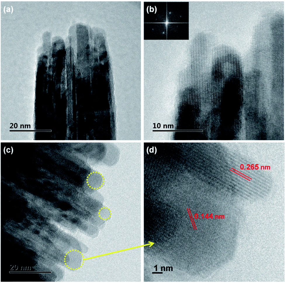 | ||
| Fig. 2 (a) TEM image and (b) HRTEM image of SnO2 NAs, the insert is SAED pattern, (c) TEM image and (d) HRTEM image of SnO2–Au NAs. | ||
The hypothetical mechanism of SnO2 NAs growth process has been proposed in the literature.18 In a ternary acidic system containing an appropriate proportion of water, ethanol and acetic acid, controlling the hydrolysis rate can make the supersaturation higher than the critical concentration of heterogeneous nucleation on the substrate and lower than the critical concentration of homogeneous nucleation in the solution. As a result, SnO2 can nucleate on the substrate. The organic ligands in solution will adsorb on the surface of the initial core, reduce the surface energy and form the nuclei of primary NRs. With the hydrolysis process, the nuclei increase in width and height, thus forming SnO2 NRs consisting of a bunch of primary NRs. The NRs continue to grow and form NAs filled with organic ligands in the middle space. The introduction of Au provides more nucleation points for SnO2 nucleation on the substrate, which makes the NAs more compact and orderly. The growth mechanism of SnO2 NAs and SnO2–Au NAs is shown in Fig. 3.
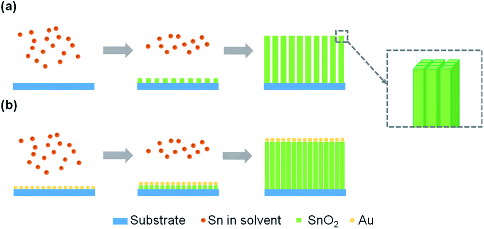 | ||
| Fig. 3 Growth mechanism diagram of (a) SnO2 NAs and (b) SnO2–Au NAs. | ||
In order to ensure good ohmic contact between the electrode and the sample in the ultraviolet detector, it is necessary to select the electrode material with appropriate work function. UPS is usually used to analyze the work function of materials. Fig. 4a and b are UPS image of SnO2 NAs and local enlargement image of cut-off and valence band edges, respectively. The work function of SnO2 NAs can be obtained from the cut-off energy according to the formula W = hv − Ecut-off, where W is work function of semiconductor, hv is photon energy and Ecut-off is cut-off energy, which can be obtained from the intersection point of the fitting line of the cut-off edge and the baseline.8,23,24 As shown in Fig. 3b, hv used in the instrument is 21.22 eV, the cut-off energy of SnO2 NAs is 16.68 eV, and the work function is 4.54 eV. Therefore, Al is chosen as the electrode material for ultraviolet detectors. In addition, the intersection point of the fitting line at the edge of the valence band and the baseline is the difference between the valence band and the Fermi level.
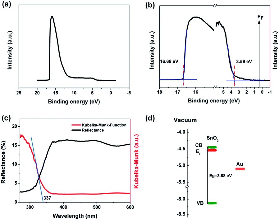 | ||
| Fig. 4 (a) UPS spectrum, (b) local UPS spectra of the cut-off region and valence band edge region, (c) UV-vis DRS spectra and (d) band structure of SnO2 NAs. | ||
As shown in Fig. 4c, UV-vis DRS is used to further characterize the band structure of SnO2 NAs. The reflectivity of SnO2 NAs is very strong in the visible band. When the wavelength is less than 350 nm, the reflectivity decreases rapidly, indicating that the samples begin to absorb light. The Kubelka–Munk formula can be used to transform the reflectivity curve, which is shown by the red line in Fig. 4c. The intersection point between the fitting line with the largest slope and the line with zero ordinate is the absorption wavelength of the sample. The absorption wavelength of SnO2 NAs is 337 nm, and the bandgap of SnO2 NAs is estimated to be about 3.68 eV. Therefore, we use UV light with a wavelength of 330 nm as excitation light of UV detectors.
According to the information obtained by UPS and UV-vis DRS, the band structure of SnO2 NAs can be drawn, as shown in Fig. 4d. The valence band (VB), Fermi level (EF) and conduction band (CB) of SnO2 NAs are −8.13 eV, −4.54 eV and −4.45 eV, respectively, relative to the vacuum level. It can be seen that the EF of n-type SnO2 NAs is very high and close to the CB, which indicates that there are many high energy electrons with high concentration.
3.2 Photoelectric properties of SnO2 NAs
The schematic diagram of UV detectors based on SnO2 and SnO2–Au NAs is illustrated in Fig. 5a. In our work, UV detectors are constructed simply and quickly by plating Al electrodes on the top of the arrays through electron beam evaporation. Fig. 5b is the current–voltage (I–V) characteristics of UV detectors under dark and light irradiation. UV light with the power of 20 μW cm−2 and wavelength of 330 nm is used as excitation light. UV irradiation can stimulate valence band electron transitions and generate electron–hole pairs, which makes the photocurrent (Iphoto) increase sharply. The Iphoto of SnO2 and SnO2–Au NAs can reach 5.49 μA and 20.03 μA, respectively, even if the bias voltage is only 1 V. With the increase of bias voltage, the Iphoto of both devices increases linearly, which indicates that good ohmic contact is formed between the Al electrode and SnO2 NAs. Compared with Iphoto, the dark current (Idark) of the two devices has little difference and almost no gain with the increase of bias voltage.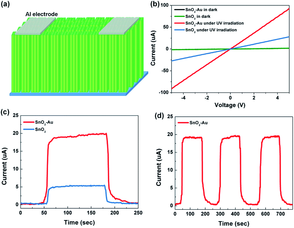 | ||
Fig. 5 (a) The schematic diagram of the fabricated UV detectors, (b) I–V characteristics curves of SnO2 and SnO2–Au NAs based devices under dark and UV irradiation, photocurrent response under on/off radiation UV light in 250 s of SnO2 and SnO2–Au NAs based device (c) and in 780 s of SnO2–Au NAs based device (d) the power density of the UV light used is 20 μW cm−2 (λ =![[thin space (1/6-em)]](https://www.rsc.org/images/entities/char_2009.gif) 330 nm), and the bias voltage is 1 V. 330 nm), and the bias voltage is 1 V. | ||
The sensitivity (S) [S = (Iphoto − Idark)/Idark] and responsivity (R) [R = Iphoto/PA, P represents the incident optical power density, A represents the effective area.] are calculated at bias voltage of 1 V, as shown in Table 1. SnO2 NAs UV detectors have high responsivity, while SnO2–Au NAs UV detectors have nearly four times higher responsivity. External quantum efficiency (EQE) is a characterization of the photon utilization rate of detectors.11 It refers to the number of electron–hole pairs produced by absorbing a photon energy per unit time. The formula for calculating EQE can be expressed as EQE = hc(Iphoto − Idark)/eλPA, where h is Planck constant, c is the speed of light, e is the unit charge, and λ is the excitation wavelength. Specific detectivity (D*) is an important figure in evaluating the performance of photodetectors,25,26 related to the signal that a detector can distinguish from the background noise. When the shot noise from dark current is considered to be the major contributor, the D* can be expressed as D* = RA1/2/(2eIdark)1/2. The EQE and D* of SnO2–Au NAs UV detectors are as high as 376321% and 1.25 × 10¹² Jones, respectively, which is about four times of pure SnO2 NAs UV detectors.
| Sample | S | R (A/W) | EQE (%) | D* (Jones) | τg (s) | τd (s) |
|---|---|---|---|---|---|---|
| SnO2 | 30 | 275 | 103145 |
3.62 × 10¹¹ | 4.3 | 5.4 |
| SnO2–Au | 110 | 1002 | 376321 |
1.25 × 10¹² |
3.7 | 5.3 |
In order to study whether the devices can respond to low-power UV light efficiently and stably under low bias voltage, and verify that the devices can be used as high-responsivity and energy-saving UV detectors, the following performance tests set the bias voltage to 1 V and the UV power to 20 μW cm−1.2 Fig. 5c exhibits the time-resolved UV Iphoto on/off measurements of SnO2 and SnO2–Au NAs UV detectors in 250 s. When the UV light is irradiated, the Iphoto rapidly rises to saturation state, and maintains a stable state. When the UV light is turned off, the Iphoto falls back rapidly. The response times of the devices listed in Table 1 are obtained by non-linear fitting of the curves, τg is the rise time constant and τd is the decay time constant. Because the primary NRs in SnO2 NAs are small in size and have many grain boundaries, although the primary NRs are in close contact, the scattering of grain boundaries still hinders the carrier migration, which makes the carrier collection rate not fast enough. Three repeated response cycles of SnO2 NAs UV detector are displayed in Fig. 5d, in which the Iphoto can keep consistent and repeatable with no significant degeneration during the whole detection process, indicating that our devices have good stability and reliability.
In order to further evaluate the performance of our SnO2–Au NAs UV detectors, the performance parameters of different SnO2 based UV detectors are compared, as shown in Table 2. It can be seen that in the similar nanostructured UV detectors, our detectors have great advantages in responsivity and EQE.
| Material | R (A/W) | EQE (%) | Iphoto/Idark | τg | τd | Reference |
|---|---|---|---|---|---|---|
| SnO2–Au nanoarrays | 1002 | 376321 |
111.3 | 3.7 s | 5.3 s | This work |
| SnO2 nanowires | 1.18 | — | 1.67 | — | — | 13 |
| SnO2 nanowires | — | 8000 | 5 | — | — | 27 |
| Au-coated SnO2 nanowires | — | 900 | — | — | — | 28 |
| Gai2O3/SnO2:Ga core–shell | — | 0.362 | 1066.7 | — | — | 15 |
| SnO2–TiO2 nanofibers | 0.6 | — | 4500 | 0.03 s | 0.01 s | 19 |
| ZnO–SnO2 nanofibers | — | — | 4600 | 32.2 s | 7.8 s | 17 |
| ZnS/SnO2 nanoparticles | 1.2 × 10⁻⁸ | — | 13.5 | 4.2 s | 1.5 s | 29 |
The reason why SnO2 NAs UV detectors exhibit higher EQE performance and the role of Au introduction will be explained in the following aspects. Compared with ordinary NRs, the SnO2 NAs composed of several primary NRs have a larger specific surface area, which can increase the scattering and absorption of UV light, thereby increasing the absorption efficiency of UV light and improving the photocurrent. At present, it is generally believed that oxygen molecules will adsorb on the surface of semiconductor oxides and capture free electrons therein,26–30 resulting in the formation of low conductivity depletion layer or space charge region (SCR) on the surface of materials. When the photon energy irradiated on the material is larger than its bandgap, photogenerated electrons and holes will be excited. The holes will separate from electrons, and then move along the potential gradient caused by the bending of the energy band to the surface of the material and combine with oxygen ions to desorb oxygen molecules. The process of adsorption and desorption of oxygen molecules is expressed as O2(g) + e− → O2−(ad), h+ + O2−(ad) → O2(g), where O2(g) denotes oxygen molecules, O2−(ad) denotes adsorbed oxygen ions, e− denotes electrons, and h+ denotes holes. Fig. 6a shows the whole process. In addition, nanostructures with large specific surface area usually exhibit a large increase in the probability of oxygen-related hole trapping and the number of surface trapped states due to a large number of suspended bonds on the surface. Therefore, the prepared SnO2 NAs can desorb more oxygen, separate photogenerated carriers and reduce their recombination, thus greatly prolonging the carrier lifetime. Because EQE can also be expressed as the ratio of carrier lifetime to transition time between electrodes, the reason why SnO2 NAs UV detectors exhibit higher EQE performance is explained.
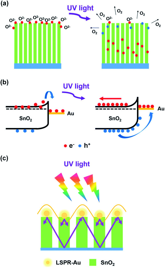 | ||
| Fig. 6 Schematic diagram of (a) oxygen absorption and desorption on SnO2 NAs surface, (b) surface energy band structure of SnO2–Au NAs, (c) surface enhanced UV absorption efficiency of Au NPs. | ||
As shown in Fig. 4d, considering that the work function of Au is larger than that of SnO2 NAs, carrier concentration and potential redistribution will occur at the interface, forming a Schottky barrier. Electrons transfer from SnO2 NAs to Au NPs attached to the surface of SnO2, and the energy band will bend, which hinders the electron transition and reduces the dark current of devices. When excited by UV light, the photogenerated holes move towards Au NPs along the bend of the energy band, while the photogenerated electrons move backward under the action of the built-in electric field, as shown in Fig. 6b. This effect further reduces the recombination of photogenerated electrons and holes, thus prolonging the carrier lifetime and further improving the EQE performance of devices.
Au NPs at the top of SnO2 NAs will inevitably increase the scattering and absorption efficiency of UV light. In addition, Au NPs can generate local surface plasmon resonance under UV excitation.31–35 The near-field amplitude will be enhanced under resonance conditions and localized on the surface of Au NPs. It can be used as an optical antenna to store UV energy in the near-field, as well as a sub-wavelength scatterer to capture and redistribute UV light onto SnO2 NAs, as shown in Fig. 6c. This effect can stimulate more photogenerated carriers, which results in high photocurrent and EQE performance of SnO2–Au NAs UV detectors.
4. Conclusions
In summary, we have fabricated a novel morphology of SnO2 NAs by a simple and controllable solvothermal method. Oxygen adsorbs on the surface of SnO2 NRs to form SCRs, which effectively separate space charges. Au NPs induce the growth of smaller and more orderly NRs. At the same time, the band bending of the interface between Au and SnO2 reduces the recombination of photogenerated electrons and holes, and the LSPR effect of Au improves the absorption efficiency of UV light. Therefore, the prepared UV detectors have high responsivity, EQE and D* to UV light with power of only 20 μW cm−2 at 1 V bias voltage, which would provide reference value for energy-saving UV detectors.Conflicts of interest
There are no conflicts to declare.Acknowledgements
This work was supported by the National Natural Science Foundation of China under Grant No. 91833301, and Zhejiang Provincial Natural Science Foundation of China under Grant no. LY17E020005.Notes and references
- E. Monroy, F. Calle, J. L. Pau, E. Muñoz, F. Omnès, B. Beaumont and P. Gibart, J. Cryst. Growth, 2001, 230, 537–543 CrossRef CAS.
- E. Muñoz, E. Monroy, J. L. Pau, F. Calle, F. Omnès and P. Gibart, J. Phys.: Condens. Matter, 2001, 13, 7115–7137 CrossRef.
- Q. Zhang, X. Li, Z. He, M. Xu, C. Jin and X. Zhou, J. Phys. D: Appl. Phys., 2019, 52, 303002 CrossRef CAS.
- Y. Zou, Y. Zhang, Y. Hu and H. Gu, Sensors, 2018, 18, 2072 CrossRef PubMed.
- Z. R. Yu and M. Aceves-Mijares, Appl. Phys. Lett., 2009, 95, 081101 CrossRef.
- E. Monroy, F. Omnès and F. Calle, Semicond. Sci. Technol., 2003, 18, R33–R51 CrossRef CAS.
- S. Mathur, S. Barth, H. Shen, J. C. Pyun and U. Werner, Small, 2005, 1, 713 CrossRef CAS PubMed.
- X. Liu, X. Liu, J. Wang, C. Liao, X. Xiao, S. Guo, C. Jiang, Z. Fan, T. Wang, X. Chen, W. Lu, W. Hu and L. Liao, Adv. Mater., 2014, 26, 7399–7404 CrossRef CAS PubMed.
- Z. R. Dai, Z. W. Pan and Z. L. Wang, Adv. Funct. Mater., 2003, 13, 9–24 CrossRef CAS.
- J. Zhao, R. Deng, J. Qin, J. Song, D. Jiang, B. Yao and Y. Li, J. Alloys Compd., 2018, 748, 398–403 CrossRef CAS.
- L. F. Hu, J. Yan, M. Y. Liao, L. M. Wu and X. S. Fang, Small, 2011, 7, 1012–1017 CrossRef CAS PubMed.
- L. Gan, M. Liao, H. Li, Y. Ma and T. Zhai, J. Mater. Chem. C, 2015, 3, 8300–8306 RSC.
- J. M. Wu and C. H. Kuo, Thin Solid Films, 2009, 517, 3870–3873 CrossRef CAS.
- J. W. Yan, Y. Chen, X. W. Wang, Y. Fu, J. X. Wang, J. Sun, G. Z. Dai, S. H. Tao and Y. L. Gao, Nanoscale, 2019, 11, 2162–2169 RSC.
- C. L. Hsu and Y. C. Lu, Nanoscale, 2012, 4, 5710–5717 RSC.
- S. Abbas, D.-K. Ban and J. Kim, Sens. Actuators, A, 2019, 293, 215–221 CrossRef CAS.
- W. Tian, T. Zhai, C. Zhang, S. L. Li, X. Wang, F. Liu, D. Q. Liu, X. K. Cai, K. Tsukagoshi, D. Golberg and Y. Bando, Adv. Mater., 2013, 25, 4625–4630 CrossRef CAS PubMed.
- S. Chen, M. Wang, J. F. Ye, J. G. Cai, Y. R. Ma, H. H. Zhou and L. M. Qi, Nano Res., 2013, 6, 243–252 CrossRef CAS.
- X. D. Li, C. T. Gao, H. G. Duan, B. G. Lu, Y. Q. Wang, L. L. Chen, Z. X. Zhang, X. J. Pan and E. Q. Xie, Small, 2013, 9, 2005–2011 CrossRef CAS PubMed.
- X. L. Xu, Y. Chen, G. H. Zhang, S. H. Yan, H. Q. Bian, Q. Chen, Y. Lu and S. Y. Ma, Mater. Lett., 2017, 195, 159–163 CrossRef CAS.
- X. Chen, K. W. Liu, Z. Z. Zhang, C. R. Wang, B. H. Li, H. F. Zhao, D. X. Zhao and D. Z. Shen, ACS Appl. Mater. Interfaces, 2016, 8, 4185–4191 CrossRef CAS PubMed.
- W. I. Park, G. C. Yi, J. W. Kim and S. M. Park, Appl. Phys. Lett., 2003, 82, 4358–4360 CrossRef CAS.
- Q. Wang, Y. C. Shao, H. P. Xie, L. Lyu, X. L. Liu, Y. L. Gao and J. S. Huang, Appl. Phys. Lett., 2014, 105, 163508 CrossRef.
- D. Cahen and A. Kahn, Adv. Mater., 2003, 15, 271–277 CrossRef CAS.
- Y. Wen, Q. S. Wang, L. Yin, Q. Liu, F. Wang, F. M. Wang, Z. X. Wang, K. L. Liu, K. Xu, T. A. Shifa, C. Jiang, J. Xiong and J. He, Adv. Mater., 2016, 28, 8051–8057 CrossRef CAS PubMed.
- J. L. Wang, H. H. Fang, X. D. Wang, X. S. Chen, W. Liu and W. D. Hu, Small, 2017, 13, 1700894 CrossRef PubMed.
- C. H. Lin, R. S. Chen, T. T. Chen, H. Y. Chen, Y. F. Chen, K. H. Chen and L. C. Chen, Appl. Phys. Lett., 2008, 93, 112115 CrossRef.
- C. Y. Chen, J. R. D. Retama, I. W. Wu, D. H. Lien, M. W. Chen, Y. Ding, Y. L. Chueh, C. I. Wu and J. H. He, ACS Nano, 2012, 6, 9366–9372 CrossRef CAS PubMed.
- C. Zhang, Y. C. Xie, H. Deng, T. Tumlin, C. Zhang, J. W. Su, P. Yu and J. Lin, Small, 2017, 13, 1604197 CrossRef PubMed.
- C. C. Wu, B. W. Du, W. Luo, Y. Liu, T. Y. Li, D. Wang, X. Guo, H. Ting, Z. Y. Fang, S. F. Wang, Z. J. Chen, Y. X. Chen and L. X. Xiao, Adv. Opt. Mater., 2018, 6, 1800811 CrossRef.
- A. Rajan, H. K. Yadav, V. Gupta and M. Tomar, Appl. Phys. A, 2014, 116, 913–919 CrossRef CAS.
- R. A. Naphade, M. Tathavadekar, J. P. Jog, S. Agarkar and S. Ogale, J. Mater. Chem. A, 2014, 2, 975–984 RSC.
- A. Polman, Science, 2008, 322, 868–869 CrossRef PubMed.
- H. A. Atwater and A. Polman, Nat. Mater., 2010, 9, 205–213 CrossRef CAS PubMed.
- T. L. Temple and D. M. Bagnall, J. Appl. Phys., 2011, 109, 084343 CrossRef.
Footnote |
| † Electronic supplementary information (ESI) available: Surface scan energy spectrum of SnO2–Au NAs. See DOI: 10.1039/c9ra03999f |
| This journal is © The Royal Society of Chemistry 2019 |