
 Open Access Article
 This Open Access Article is licensed under a Creative Commons Attribution-Non Commercial 3.0 Unported Licence
Study on photoelectric characteristics of monolayer WS2 films
Lin Wanga,
Wenyan Wanga,
Quan Wanga,
Xiaochun Chi*a,
Zhihui Kanga,
Qiang Zhoub,
Lingyun Pana,
Hanzhuang Zhanga and
Yinghui Wang *a
*a
aFemtosecond Laser Laboratory, Key Laboratory of Physics and Technology for Advanced Batteries (Ministry of Education), College of Physics, Jilin University, Changchun 130012, P. R. China. E-mail: wangyinghuijlu@outlook.com
bState Key Laboratory of Superhard Materials, College of Physics, Jilin University, Changchun 130012, P. R. China
First published on 14th November 2019
Abstract
It is important to determine the time-dependent evolution of the excited monolayer WS2, which will provide a basis for the reasonable design of optoelectronic devices based on two-dimensional transition metal dichalcogenides. Here, we made a simple and large-area photodetector based on the monolayer WS2, with high light sensitivity and fast response, benefiting from the special dynamics of carrier involving the exciton, trion, and charge. Moreover, we tested the relaxation behavior of the excited monolayer WS2 by employing transient absorption (TA). It was found that the multi-body interaction among exciton would occur after the density of pump photon increases to 3.45 × 10¹⁴ photons per cm2. The exciton dissociation accompanying the generation of trion would appear in the photo-induced relaxation process, which would be a benefit for the operation of this photodetector. Increasing the energy of the exciton is good for the generation of carrier by comparing the relaxation behavior of WS2 excited to A and B exciton states. However, the bound exciton relaxation, originating from the capture process of the defect state, would exist and play an unfavorable role during the functioning of devices.
Introduction
Since the monolayer of graphene has been applied extensively in the optoelectronic fields, the atomically thin materials have been receiving much attention.1 The family of semiconducting transition metal dichalcogenides (TMDCs), involving MoS2,2 WS2,3 MoSe2, and MoTe2,4 have highlighted an increasingly important role, owing to their intriguing physical properties, such as their sub-nanometer thickness, large optical absorbance, and sizable bandgaps around 1–2 eV.5,6 The extremely thin thickness of TMDCs makes the control of switching more effective,7 which can support high on/off ratios and can help in reducing the short-channel effects and power dissipation. These advantages of TMDCs are very convenient for developing field-effect transistors (FETs)8 and other optoelectronic devices.9 Recently, it has been proven that the superiority of OFF-state current in the depletion regime10 would allow the photodetectors, based on TMDCs, to have excellent characteristics, such as low-noise and high-sensitivity detection.11,12In order to broaden the application of TMDCs in the optoelectronic fields, people need to improve the photoelectric performances and simplify the fabrication process of devices based on the understanding of the carrier dynamics. Actually, both of them depend on the understanding of the ultrafast physical process occurring in the TMDCs. Recently, many ultrafast photo-induced phenomena occurring in TMDCs have been explored, such as phonon scattering,13 photo-generated carrier relaxation,14–21 exciton–exciton interactions,22–25 strong light-matter interactions,26 and carrier mobility,27 which would play an important role in various optoelectronic applications such as solar cells28 and photodetectors.29 Indeed, they open a new window to understand the behaviour of photo-excitation dynamics occurring in semiconductors and broaden a new path to fabricate a new optoelectronic device.
In this letter, we fabricated a large-area and fast-response photodetector based on monolayer WS2 through a simple method and tested its optoelectronic performance simultaneously. Moreover, we probed the corresponding ultrafast photoinduced relaxation process of monolayer WS2 by using femtosecond transient absorption. From our data, we differentiated multiple dynamic processes in the excited WS2 and analyzed their role in the performance of the photodetector simultaneously. The understanding of the carrier dynamics helps us to analyze the operation mechanism of the devices based on monolayer WS2.
Results and discussion
Materials and basic characterization
The monolayer WS2, in our experiment, was grown on the sapphire substrates by the CVD (chemical vapour deposition) technique.30 The steady-state absorption was measured by a UV-vis absorption spectrometer (Purkinje, TU-1810PC). The femtosecond laser pulse was generated from our laser system (Coherent), and the transient absorption technique has been reported elsewhere.31 The excitation pulse was originated from the pump optical parameters amplifier (Coherent, TOPAS), and the corresponding wavelength was estimated to be 510 nm (2.45 eV) and 610 nm (2.03 eV), respectively.32 The Raman spectrum was recorded using a Renishaw in Via Raman Microscopic instrument. Excitation laser at 514 nm was obtained with a Spectra-Physics 160 M argon-ion laser. In the fabrication of the photodetector, we used thermal-evaporator (Technol, ZHD 300) deposited two silver electrodes on the monolayer WS2, with a thickness of 1000 Å and the electrode gap was about 50 μm. The absorption spectrum in Fig. 1 shows the typical spectral features of monolayer WS2 on the sapphire substrate. There are two exciton transitions in the spectrum named “A” and “B” exciton, which originated from the spin–orbit splitting of the valence band, thereby corresponding to the excitonic transitions at the K-point of the Brillouin zone.33 The second derivative of the absorption spectrum was used to accurately determine the peak position for the oscillator strengths of A and B exciton, which is shown in arbitrary units with an offset for clarity.34 The final spectral results exhibit the oscillator strengths of A and B exciton, which was found to be located at 2.07 and 2.45 eV, respectively. The Raman spectrum is shown in the inset of Fig. 1, which involves two Raman peaks, corresponding to the E2g and A1g modes located at ∼355.0 and ∼418.0 cm−1, respectively. The former peak originated from the plane vibration mode of W and S atoms, while the latter one was attributed to the out-of-plane vibration of the S atoms.35,36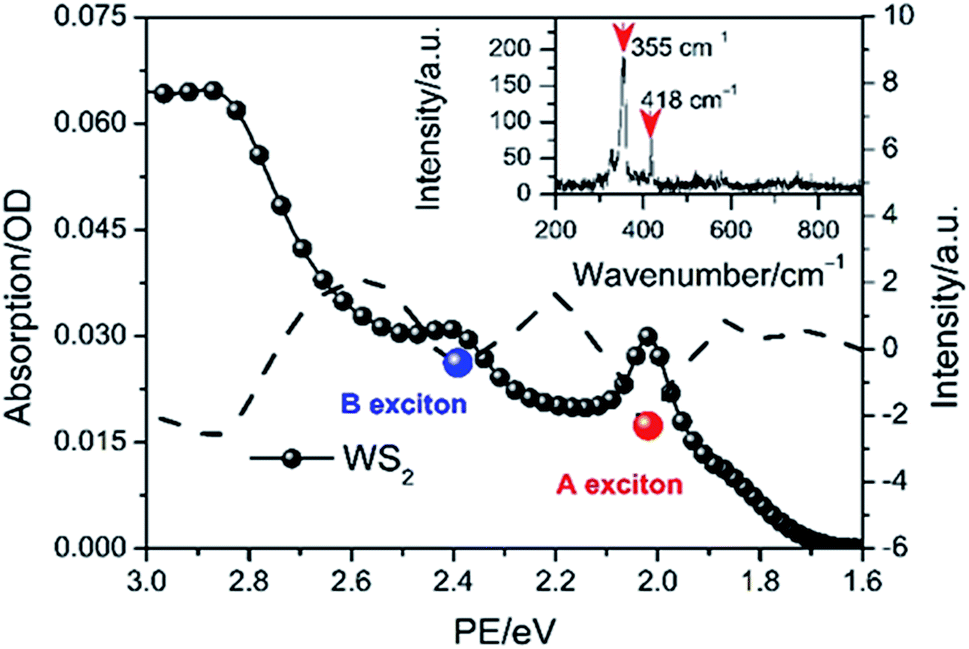 | ||
| Fig. 1 The absorption spectrum of the monolayer WS2 and its second derivative (the dashed line). Inset: the Raman spectra of WS2. | ||
Photodetector performance
We carried out a series of optoelectronic tests on the photodetector to analyze its performance. Fig. 2(a) exhibits the illumination intensity-dependent photocurrent curve during the repetitive switching of light illumination. The laser wavelength was about 532 nm, and the bias voltage was fixed at −10 V. The photocurrent showed no obvious degradation during the scores of cycles, suggesting that our photodetector had good stability and repeatability. It implies that the carrier diffusion process under different illumination intensities but with the same voltage was much rapid. Fig. 2(b) further indicates that the photocurrent of the device increases almost linearly with the illumination intensity, thereby suggesting that the generation yield of the photo-generated carriers was almost insensitive to the illumination intensity when the bias voltage was fixed. The intercept was estimated to be 0.08 nA through linear fitting, indicating that the pure electronic field would drive the movement of carriers without illumination. Herein, some free carriers exist in the monolayer of WS2 at room temperature and were responsible for the photocurrent under the bias voltage. In addition, the responsivity of the device decreased with the illumination intensity and is gradually close to the extreme and towards stability after the illumination intensity was increased to 60 mW mm−2 (as seen in Fig. 2(b)), showing the good light responsiveness of our photodetector.37,38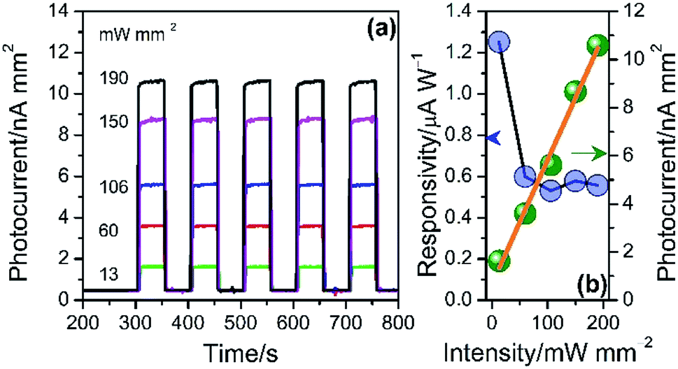 | ||
| Fig. 2 (a) Photocurrent of monolayer WS2 under 532 nm excitation with different illumination intensities at the voltage of 10 V. (b) Plot of photocurrent and responsivity at different illumination intensities. | ||
Fig. 3(a) offers the evolution of photocurrent as a function of bias voltage. Apparently, the base current (I0) and the photocurrent (ΔI) together increased with the bias voltage. The former implies that the improvement of I0 should originate from the enhancement of the carrier mobility rate since the room temperature was invariable, and the population of the free carriers, activated by temperature, remain unchanged. In addition, the enhancement of the current originating from the variance of the carrier mobility rate was very limited. Therefore, the increase in the photocurrent (ΔI) at different bias voltage should depend very much on the improvement of the free carrier yield and the enhancement of the carrier mobility, since the illumination intensity was invariable. Fig. 3(b) is the plot of ΔI with different bias voltage under the same illumination intensity. As it is shown, the free carriers increased almost linearly with the bias voltage, suggesting that the carrier yield does not reach saturation. The ratio of the voltage to the response photocurrent can be represented in terms of the resistance of the photodetector, and it was found that the ratio decreases as the bias voltage decreases. In addition, we also extracted the rise and decay time from the temporal response curve, which were shorter than 2 s but much faster than the devices of the same scale reported before.39
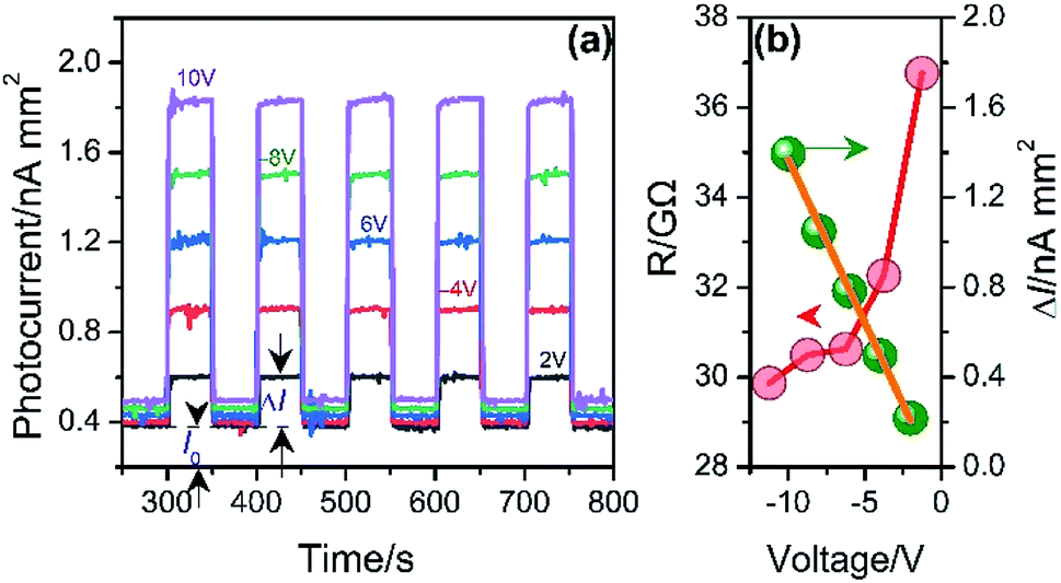 | ||
| Fig. 3 (a) Photocurrent of monolayer WS2 under 532 nm excitation and the illumination intensity was fixed at 13 mW mm−2. (b) Plot of ΔI and resistance (R) at different voltage. | ||
Ultra-fast carrier dynamics
In order to clearly scan the carrier dynamics occurring in the monolayer WS2 of the photodetector, the corresponding transient absorption data was obtained and is given in Fig. 4. The WS2 thin film used in the TA test was the same as that in the photodetector. Further, to study the photodetector characteristics, we used CW-laser. In the TA test, we employed the femtosecond laser. As per the previous reports,40–42 the carrier dynamics probed by the TA technique was the same as that induced by the CW-laser, since the generation of the carrier was independent of the CW-laser or a femtosecond laser. The initial TA spectrum in Fig. 4(a) offers a spectral feature of monolayer WS2 at 0.3 ps, involving three positive bands (located at 2.03, 2.41, and 2.89 eV) and three negative bands (1.90, 2.24, and 2.67 eV), corresponding to the different exciton transitions. The former was attributed to the ground state bleaching (GSB) of A, B, and C exciton transition that mirrors the absorption spectrum in Fig. 1, and the latter was assigned to the photon-induced absorption (PIA) of the exciton transition as mentioned above. According to the band structure of WS2 (inset of Fig. 4(a)), we employed five Gaussian peaks to fit the TA spectra, so as to build the relationship between the spectral feature and the electronic transition, and further determined the origin of PIA simultaneously. The negative bands at 2.26 eV and 1.9 eV should correspond to the PIA of the C exciton state and that at 2.67 eV should originate from the PIA of A/B exciton according to the band structure.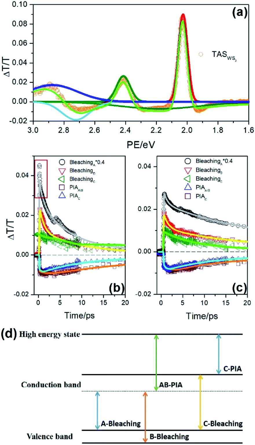 | ||
| Fig. 4 (a) The TA spectra of WS2 at initial time. The dynamic curves corresponding to the spectral features in the initial TA spectra, and the fitting line of WS2 excited by photon with energy of 2.07 (b) and 2.45 eV (c). (d) The theoretical predicted energy band structure corresponding to the direct transitions of monolayer WS2. | ||
Fig. 4(b) offers the wavelength-dependent decay curves of WS2, excited with A exciton resonance, with all the curves being fitted with a multi-exponential function. After photoexcitation, a sub-picosecond decay process marked with red lines was observed in A bleaching, which was too fast to be distinguished in our experiment. The illumination intensity-dependent decay behaviour has been observed in other TMDCs, such as MoS2 and MoSe2, which involve a much rapid decay process originating from the strong exciton–exciton annihilation.43,44 Considering the similarity in the time scale, it was speculated that the rapid relaxation component should be assigned to the exciton–exciton annihilation45 among A excitons. For the decay curve of B bleaching, there also exists a fast-initial decay component, whose lifetime was close to 1 ps. This component can be attributed to the capture of the exciton originating from the defect state,46,47 which often exists in the large surface area of the two-dimensional materials with many dangling bonds. In addition, this type of trapping states often appears in the semiconductor with nanoscale.48
After that the bound exciton in the defect state would gradually annihilate. A little rising component with a lifetime of 0.5 ps appears at 2.70 eV (AB-PIA), indicating that the A and B exciton would dissociate into carriers after photon-excitation, which should accompany with the generation of trion in the monolayer WS2. It is interesting to find that the kinetic curves at 2.89 eV (C bleaching) and 2.26 eV (C-PIA) do not exhibit a fast relaxation component with a lifetime of 1.0 ps, thereby suggesting that the C exciton, with high activity, was not captured by the defect state, and thus might directly dissociate into the carriers after photoexcitation.49 After 5 ps, the amplitude of all the spectral features in the TA spectra decreased with time, suggesting that the excitons or carriers in the monolayer WS2 would gradually migrate or recombine in the monolayer WS2 with time. If the monolayer of WS2 was excited with the B exciton resonance, the corresponding relaxation behavior (as seen in Fig. 4(c)) would have been a little different in comparison with that of the A excitonic transition. At the same photon density, the rapid sub-picosecond relaxation component would disappear in the kinetic curve at 2.03 eV (A bleaching). But the fast process, with which the lifetime of 1.0 ps illustrates the capture of exciton by the defect state, would still appear in the TA curve at 2.41 and 2.03 eV (A bleaching), suggesting that the defect state would still participate in the photo-induced relaxation process. In addition, both A and B excitons would dissociate into the carriers, accompanied by the formation of trion,50 since there is a rising component in the TA curve at 2.70 eV (AB-PIA). According to the present data, it is reasonable to speculate that the exciton dissociation accompanying the generation of trion should play a positive role in the performance of our photodetector based on WS2, but the process of exciton capture by the defect state would lead to the retroaction. Further, the exciton–exciton interaction that would exist at high illumination intensity may not happen since the density of the exciton would not be too high during the operation of the photodetector. The illumination intensity-dependent TA data are summarized in Fig. 5, where the pump influence increases from 3.45 × 10¹⁴ to 4.14 × 10¹⁵ photons per cm2. Fig. 5(a) and (b) offer the illumination intensity-dependent TA curves at 2.03 eV (A bleaching) and 2.41 eV (B bleaching) under the pump photon energy of 2.03 eV. As mentioned above, the rapid (sub-picosecond) component, marked with the red square, originated from the exciton–exciton interaction. Herein, the intensity-dependent TA amplitude also confirmed this view, but the corresponding lifetime was too short to be distinguished, suggesting that the interaction among the excitons in the monolayer of WS2 was much rapid.51 Note that there was no rapid relaxation component in Fig. 5(b), suggesting that the exciton–exciton interaction would not happen among B exciton. However, the capture process of B exciton by the defect state still exists, whose lifetime was about 1 ps and almost invariable with the illumination intensity, as seen in Fig. 5(d). Meanwhile, the relaxation rate enhanced evidently at the same time. In addition, the variance relative to the initial amplitude of A or B exciton as a function of illumination intensity is summarized in Fig. 5(d). The amplitude of A and B exciton increases with the illumination intensity and both of them gradually become saturated. In this situation, the amplitude of B exciton would reach saturation much earlier than that of A exciton. For B exciton, its population would keep a certain range. The illumination intensity-dependent TA curve at 2.70 eV, which is resonant with AB-PIA, is also given in Fig. 5(c). The initial amplitude should be proportional to the photo-generated exciton population, and the subsequent rising behavior should correspond to the A/B exciton dissociation accompanying the formation of trion. Note that a rising component appears when the intensity increases to 6.89 × 10¹⁴ photons per cm2. Moreover, its amplitude and lifetime were obtained through multi-exponential function fitting, and both of them were sensitive to the density of photon, as seen in Fig. 5(e). The former corresponds to the sum of the amplitude of carrier (corresponding to the yield of free charge) and that of the exciton (relative to the remaining exciton). Apparently, the yield of exciton dissociation (A carrier in Fig. 5(e)) increases with the illumination intensity and gradually reaches a maximum at 4.14 × 10¹⁵ photons per cm2. For the remaining exciton (A exciton in Fig. 5(e)), its population gradually reaches a maximum and then decreases with the illumination intensity, as seen in Fig. 5(e). The lifetime of the exciton dissociation accompanying the generation of trion is also given in Fig. 5(e) (lifetime), which quickly accelerates to 2 ps with the illumination intensity. After the density of the photon increases to 1.0 × 10¹⁵ photons per cm2, the lifetime becomes 1.0 ps and is almost invariable to the illumination intensity, suggesting that the exciton dissociation dynamics reaches the saturation. Apparently, the enhancement of the pump intensity would increase the temperature and the number of photo-generated excitons. Both of them would promote the movement of carriers and facilitate the dissociation of the mount exciton.
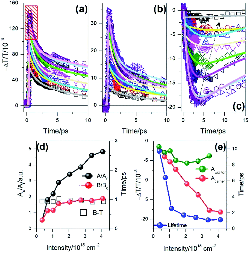 | ||
| Fig. 5 Illumination intensity-dependent (a) A exciton bleaching dynamics; (b) B exciton bleaching dynamics; (c) PIA of A/B exciton in the monolayer WS2 excited by the photon of 2.03 eV, where the black square, red circle, blue triangle, pink triangle, green square, yellow triangle, brown triangle, purple circle corresponds to the intensity of 3.45 × 10¹⁴, 6.89 × 10¹⁴, 1.03 × 10¹⁵, 1.38 × 10¹⁵, 2.07 × 10¹⁵, 2.76 × 10¹⁵, 3.45 × 10¹⁵, 4.14 × 10¹⁵ photons per cm2. (d) Initial amplitude (sold circle) of A (black) and B (red) exciton as a function of intensity. Additionally, the trapping lifetime of B exciton (square) as a function of intensity. (e) The PIA amplitude (green solid circle), the corresponding dissociated carriers (red solid circle), and the dissociation lifetime of A/B exciton at different intensities (blue solid circle). | ||
Conclusions
In summary, we fabricated a simple optoelectronic detector based on the monolayer of WS2. Through changing the illumination intensity and bias voltage, the electronic test exhibits that this photo-detector owns high-sensitivity and low-noise, implying that the photo-generated carrier dynamics would play an important role in the performance of the device. Then, the time-dependent optical response of WS2 monolayers was scanned by the femtosecond broadband transient absorption spectroscopy. It was found that the exciton–exciton annihilation, exciton dissociation, bound exciton relaxation relative to exciton trapping, and free carrier movement would participate in the relaxation process of the excited WS2 monolayer after photo-excitation. The exciton dissociation, accompanying the formation of trion, is helpful for the performance of the devices. Specifically, we found that the process of capturing exciton by the defect state and the subsequent bound exciton relaxation would also appear in the photo-induced relaxation process owing to the special structure of the two-dimensional materials, where many defect states would exist. Thus, the final results help us to understand the determination of exciton dynamics in monolayer WS2, which is of importance from the viewpoint of fundamental physics and photonic device applications.Conflicts of interest
There are no conflicts to declare.Acknowledgements
This work was supported by the National Natural Science Foundation of China (No. 21573094, 11774112, 11574112, 11904123 and 61575079).Notes and references
- K. S. Novoselov, D. Jiang, F. Schedin, T. J. Booth, V. V. Khotkevich, S. V. Morozov and A. K. Geim, Proc. Natl. Acad. Sci. U. S. A., 2005, 102, 10451–10453 CrossRef CAS PubMed.
- B. Radisavljevic, A. Radenovic, J. Brivio, V. Giacometti and A. Kis, Nat. Nanotechnol., 2011, 6, 147–150 CrossRef CAS PubMed.
- Q. H. Wang, K. Kalantar-Zadeh, A. Kis, J. N. Coleman and M. S. Strano, Nat. Nanotechnol., 2012, 7, 699–712 CrossRef CAS PubMed.
- J. Kang, S. Tongay, J. Zhou, J. Li and J. Wu, Appl. Phys. Lett., 2013, 102, 012111 CrossRef.
- J. A. Wilson and A. D. Yoffe, Adv. Phys., 1969, 18, 193–335 CrossRef CAS.
- A. D. Yoffe, Annu. Rev. Mater. Res., 1973, 3, 147–170 CrossRef CAS.
- J. P. Colinge, Solid-State Electron., 2004, 48, 897–905 CrossRef CAS.
- S. Chuang, C. Battaglia, A. Azcatl, S. Mcdonnell, J. S. Kang and X. Yin, Nano Lett., 2014, 14, 1337 CrossRef CAS PubMed.
- A. R. Klots, A. K. Newaz, B. Wang, D. Prasai, H. Krzyzanowska and J. Lin, Sci. Rep., 2014, 4, 6608 CrossRef CAS PubMed.
- H. Wang, C. Zhang, W. Chan, S. Tiwari and F. Rana, Nat. Commun., 2015, 6, 8831 CrossRef CAS PubMed.
- Q. H. Wang, K. Kalantar-Zadeh, A. Kis, J. N. Coleman and M. S. Strano, Nat. Nanotechnol., 2012, 7, 699–712 CrossRef CAS PubMed.
- H. Tian, M. L. Chin, S. Najmaei, Q. Guo, F. Xia, H. Wang and M. Dubey, Nano Res., 2016, 9, 1543–1560 CrossRef CAS.
- K. Kaasbjerg, K. S. Thygesen and K. W. Jacobsen, Phys. Rev. B: Condens. Matter Mater. Phys., 2012, 85, 115317 CrossRef.
- T. Korn, S. Heydrich, M. Hirmer, J. Schmutzler and C. Schüller, Appl. Phys. Lett., 2011, 99, 102109 CrossRef.
- R. Wang, B. A. Ruzicka, N. Kumar, M. Z. Bellus, H. Y. Chiu and H. Zhao, Phys. Rev. B: Condens. Matter Mater. Phys., 2012, 86, 045406 CrossRef.
- N. Kumar, J. He, D. He, Y. Wang and H. Zhao, J. Appl. Phys., 2013, 113, 133702 CrossRef.
- H. Shi, R. Yan, S. Bertolazzi, J. Brivio, B. Gao, A. Kis, D. Jena, H. G. Xing and L. Huang, ACS Nano, 2013, 7, 1072–1080 CrossRef CAS PubMed.
- Q. Cui, F. Ceballos, N. Kumar and H. Zhao, ACS Nano, 2014, 8, 2970–2976 CrossRef CAS PubMed.
- H. Wang, C. Zhang and F. Rana, Nano Lett., 2014, 15, 339 CrossRef PubMed.
- G. Moody, C. KavirDass, K. Hao, C. H. Chen, L. J. Li, A. Singh and E. Malic, Nat. Commun., 2015, 6, 8315 CrossRef CAS PubMed.
- C. Poellmann, P. Steinleitner, U. Leierseder, P. Nagler, G. Plechinger, M. Porer and R. Huber, Nat. Mater., 2015, 14, 889 CrossRef CAS PubMed.
- S. Sim, J. Park, J. G. Song, C. In, Y. S. Lee, H. Kim and H. Choi, Phys. Rev. B: Condens. Matter Mater. Phys., 2013, 88, 075434 CrossRef.
- N. Kumar, Q. Cui, F. Ceballos, D. He, Y. Wang and H. Zhao, Phys. Rev. B: Condens. Matter Mater. Phys., 2014, 89, 991–1000 Search PubMed.
- S. Mouri, Y. Miyauchi, M. Toh, W. Zhao, G. Eda and K. Matsuda, Phys. Rev. B: Condens. Matter Mater. Phys., 2014, 90, 155449 CrossRef.
- D. Sun, Y. Rao, G. A. Reider, G. Chen, Y. You, L. Brézin and T. F. Heinz, Nano Lett., 2014, 14, 5625–5629 CrossRef CAS PubMed.
- Q. H. Wang, K. KalantarZadeh, A. Kis, J. N. Coleman and M. S. Strano, Nat. Nanotechnol., 2012, 7, 699–712 CrossRef CAS PubMed.
- A. S. Mayorov, R. V. Gorbachev, S. V. Morozov, L. Britnell, R. Jalil, L. A. Ponomarenko and A. K. Geim, Nano Lett., 2011, 11, 2396–2399 CrossRef CAS PubMed.
- B. Peng, P. K. Ang and K. P. Loh, Nano Today, 2015, 10, 128–137 CrossRef CAS.
- S. Yang, S. Tongay, Q. Yue, Y. Li, B. Li and F. Lu, Sci. Rep., 2014, 4, 5442 CrossRef CAS PubMed.
- M. Lan, Y. Zhang, H. Song, X. Wang, C. Liu and Y. Guo, Appl. Phys. Lett., 2016, 108, 136805 CrossRef.
- Q. H. Liu, Y. Wang, N. Sui, Y. Wang, X. C. Chi, Q. Wang and H. Z. Zhang, Sci. Rep., 2016, 6, 29442 CrossRef CAS PubMed.
- X. C. Chi, P. Lu, Y. Gao, Y. H. Wang, N. Sui, M. C. Ni and H. Z. Zhang, J. Lumin., 2018, 204, 327–332 CrossRef CAS.
- A. Carvalho, R. M. Ribeiro and A. H. Castro Neto, Phys. Rev. B: Condens. Matter Mater. Phys., 2013, 88, 115205 CrossRef.
- M. Okano, H. Hagiya, T. Sakurai, K. Akimoto, H. Shibata, S. Niki and Y. Kanemitsu, Appl. Phys. Lett., 2015, 106, 181903 CrossRef.
- Y. Guo, W. Zhang, H. Wu, J. Han, Y. Zhang, S. Lin, C. Liu, K. Xu, J. Qiao, W. Ji, Q. Chen, S. Gao, W. Zhang, X. Zhang and Y. Chai, Sci. Adv., 2018, 4, 6252 CrossRef PubMed.
- J. Liang, X. Li, B. Pan, L. Zhang, Y. Dong, C. Zou and S. Huang, 2D Mater., 2019, 6, 025003 CrossRef CAS.
- R. K. Chowdhury, R. Maiti, A. Ghorai, A. Midya and S. K. Ray, Nanoscale, 2016, 8, 13429–13436 RSC.
- H. J. W. Li, K. Huang and Y. Z. Zhang, Mater. Res. Express, 2018, 6, 045902 CrossRef.
- J. D. Yao, Z. Q. Zheng, J. M. Shao and G. W. Yang, Nanoscale, 2015, 7, 14974–14981 RSC.
- J. Yang, K. Liu, Z. Cheng, P. Jing, Q. Ai, X. Chen and D. Shen, ACS Appl. Mater. Interfaces, 2018, 10(40), 34744–34750 CrossRef CAS PubMed.
- D. B. Velusamy, M. A Haque, M. R Parida, F. Zhang, T. Wu, O. F. Mohammed and H. N. Alshareef, Adv. Funct. Mater., 2017, 27(15), 1605554 CrossRef.
- K. Zhang, L. Lv, X. Wang, Y. Mi, R. Chai, X. Liu and H. Huang, ACS Appl. Mater. Interfaces, 2018, 10(2), 1917–1924 CrossRef CAS PubMed.
- D. Sun, Y. Rao, G. A. Reider, G. Chen, Y. You, L. Brézin and T. F. Heinz, Nano Lett., 2014, 14, 5625–5629 CrossRef CAS PubMed.
- N. Kumar, Q. Cui, F. Ceballos, D. He, Y. Wang and H. Zhao, Phys. Rev. B: Condens. Matter Mater. Phys., 2014, 89, 125427 CrossRef.
- B. Zhu, X. Chen and X. Cui, Sci. Rep., 2015, 5, 9218 CrossRef PubMed.
- F. Ceballos, Q. Cui, M. Z. Bellus and H. Zhao, Nanoscale, 2016, 8, 11681–11688 RSC.
- J. He, D. He, Y. Wang, Q. Cui, F. Ceballos and H. Zhao, Nanoscale, 2015, 7, 9526–9531 RSC.
- M. Amani, D. H. Lien, D. Kiriya, J. Xiao, A. Azcatl and J. Noh, Science, 2015, 350(6264), 1065–1068 CrossRef CAS PubMed.
- C. Ruppert, A. Chernikov, H. M. Hill, A. F. Rigosi and T. F. Heinz, Nano Lett., 2017, 17, 644–651 CrossRef CAS PubMed.
- C. C. Shen, Y. T. Hsu, L. J. Li and H. L. Liu, Appl. Phys. Express, 2013, 6, 125801 CrossRef.
- R. K. Chowdhury, S. Nandy, M. Karmakar, S. N. Bhaktha, P. K. Datta and S. K. Ray, 2D Mater., 2018, 6, 015011 CrossRef.
| This journal is © The Royal Society of Chemistry 2019 |