
 Open Access Article
 This Open Access Article is licensed under a Creative Commons Attribution-Non Commercial 3.0 Unported Licence
Charge balance control of quantum dot light emitting diodes with atomic layer deposited aluminum oxide interlayers†
Hoseok Jina,
Hyungseok Moona,
Woosuk Leea,
Hyeok Hwangboa,
Sang Heon Yonga,
Ho Kyoon Chungb and
Heeyeop Chae *ab
*ab
aSchool of Chemical Engineering, Sungkyunkwan University, Suwon, 16419, Republic of Korea. E-mail: hchae@skku.edu
bSKKU Advanced Institute of Nanotechnology, Sungkyunkwan University, Suwon, 16419, Republic of Korea
First published on 15th April 2019
Abstract
We developed a 1.0 nm thick aluminum oxide (Al2O3) interlayer as an electron blocking layer to reduce leakage current and suppress exciton quenching induced by charge imbalance in inverted quantum dot light emitting diodes (QLEDs). The Al2O3 interlayer was deposited by an atomic layer deposition (ALD) process that allows precise thickness control. The Al2O3 interlayer lowers the mobility of electrons and reduces Auger recombination which causes the degradation of device performance. A maximum current efficiency of 51.2 cd A−1 and an external quantum efficiency (EQE) of 12.2% were achieved in the inverted QLEDs with the Al2O3 interlayer. The Al2O3 interlayer increased device efficiency by 1.1 times, increased device lifetime by 6 times, and contributed to reducing efficiency roll-off from 38.6% to 19.6% at a current density up to 150 mA cm−2. The improvement of device performance by the Al2O3 interlayer is attributed to the reduction of electron injection and exciton quenching induced by zinc oxide (ZnO) nanoparticles (NPs). This work demonstrates that the Al2O3 interlayer is a promising solution for charge control in QLEDs and that the ALD process is a reliable approach for atomic scale thickness control for QLEDs.
Introduction
Colloidal quantum dots (QDs) are attracting attention as a promising light emitting material for optoelectronic devices due to their high color purity, high quantum yield and low cost solution processing.1–3 QDs have been widely applied in many applications such as solar cells, light emitting diodes and biological applications.4–8 QDs are particularly applicable to display and lighting devices because the emission wavelength can be easily shifted depending on the size, shape, and composition of the QDs.9–13 The device performance of the state-of-the-art QLEDs is comparable to that of commercially available organic light emitting diodes (OLEDs).14–17 However, the stability of QLEDs lags behind that of OLEDs and it needs to be overcome for commercialization.The efficiency and stability of QLEDs are known to be strongly dependent on Auger recombination.18–20 Auger recombination, a non-radiative decay process, is an exciton quenching mechanism in which extra carriers absorb exciton energy. The exciton quenching reduces device efficiency, induces efficiency roll-off and shortens device lifetime. Auger recombination is caused by the imbalance of the charge mobility in transport layers.11–14 Electron mobility of ZnO NPs electron transport layers (ETL) is known to be faster than the hole mobility of hole transport layers (HTL) in QLEDs.14
Several approaches are proposed to enhance the efficiency and stability of QLEDs by controlling electron injection. Adopting composition of QDs,21 modifying surface ligands22 or introducing extra shell of the core/shell/shell structure of QDs effectively suppress efficiency roll-off behavior.19 Various thin interlayers were introduced to improve the charge balance by suppressing electron injection with poly(methyl methacrylate),14 polyethylenimine ethoxylated (PEIE),15 polyethylenimine (PEI),23 polyfluorene derivatives,24 and soluble Al2O3.22 Organic materials are sensitive to oxygen and moisture than inorganic materials and decrease stability of QLEDs. All organic and inorganic interlayers have been formed with solution processes so far.14,15,23,25 Thickness control in atomic-scale of interlayer is absolutely important because it forms tunneling barrier in the device. However, it is challenging to control the atomic scale thickness with the solution processes.
In this study, we introduced the inorganic Al2O3 interlayer between ETL and emitting layer (EML) as the electron blocking layer by a spatially-resolved ALD process that allows for a precisely controlled thickness. ALD processes can form thin conformal films and provide good uniformity and precise thickness control.26,27 The thickness effect of Al2O3 interlayer on device efficiency and lifetime was investigated in inverted QLEDs.
Experimental
Inverted QLEDs fabrication
The device with a conventional structure is not suitable in our work due to QDs degradation by plasma in the spatially-resolved ALD process (Fig. S1†). Inverted QLEDs made in this work consists of indium tin oxide (ITO)/ZnO/Al2O3/QDs/PEIE/poly(N,N′-bis(4-butylphenyl)-N,N′-bis(phenyl)benzidine (poly-TPD)/MoOx/Al as shown in Fig. 1a15,33 and the band energy levels of each materials are shown in Fig. 1b. UV-visible absorption spectra and ultraviolet photoelectron spectra of QDs, poly-TPD and ZnO NPs are illustrated in Fig. S2 and S3.† A patterned ITO on glass substrate was cleaned sequentially with acetone and methanol. A 70 nm-thick ZnO NPs (80 mg ml−1, in ethanol) ETL was spin-coated at 1500 rpm for 30 s and baked at 150 °C. The Al2O3 interlayers from 0 to 3.0 nm were deposited on ZnO NPs layers by a spatially-resolved ALD process. A 25 nm-thick CdSe@ZnS/ZnS QDs (in hexane/octane, OD = 1.5), a 7.5 nm thick-PEIE (in 2-methoxyethanol, 0.5 wt%), a 40 nm-thick poly-TPD HTL (in chlorobenzene, 10 mg ml−1) and a 10 nm-thick MoOx hole injection layer (in acetonitrile, 10 mg ml−1) were spin-coated at 3000 rpm for 30 s and baked at 150 °C sequentially. (MoO3)12·H3PO4·(H2O)x (PMAH) solution (in acetonitrile, 10 mg ml−1) was stirred for 10 min at 60 °C and filtered through polyvinylidene fluoride (PVDF) membrane before the spin-coating. All layers were deposited and baked in a nitrogen-filled glove box (H2O < 1 ppm). Finally, Al electrodes (100 nm) were deposited by a thermal evaporation process under high vacuum of ∼6 × 10⁻⁶ torr. | ||
| Fig. 1 (a) The schematic structure of the QLED with Al2O3 interlayer between QDs and ZnO, (b) band energy level diagram of each materials, (c) the schematic view of the sequential procedure of spatially-resolved ALD process. | ||
Deposition of Al2O3 interlayer by spatially-resolved ALD process
The Al2O3 interlayer was formed by trimethylaluminum (TMA) as an aluminum precursor and N2O plasma as an oxygen radical precursor. TMA with Ar carrier gas and N2O plasma are supplied to source and plasma zone. The sequential procedure of spatially-resolved ALD process are shown Fig. 1c. Each zone is separated by adjacent purge zones to prevent gas mixing and the gap between moving substrate and gas supplied head is less than 2 mm. The gas flowrate of TMA precursor with Ar carrier gas and N2O precursor are 50 and 20 sccm. The Al2O3 interlayer was deposited on the devices at the substrate temperature of 80 °C with the plasma power of 150 W. Substrate moving speed is 125 mm s−1 and the growth per cycle of spatially-resolved ALD process is 1.0 Å per cycle. Binding energy and atomic concentration of Al2O3 deposited by spatially-resolved ALD process are shown in Fig. S4.†Characterizations
Absorption spectra was taken with a UV/visible spectrophotometer (JASCO, V630). PL emission spectra was obtained by a Cary Eclipse fluorescence spectrophotometer (Agilent Technologies, G9803AA). The diameters of QDs and ZnO NPs were determined by a Cs-corrected high-resolution transmission electron microscopy (HRTEM) with an accelerating voltage 200 kV (JEOL, JEM-ARM 200F). X-ray diffraction pattern was taken with an X-ray diffractometer (Bruker Corporation, D8 ADVANCE). Surface roughness was measured by high-resolution atomic force microscope (SII Nanotechnology, SPA-300HV). Band energy levels of each materials were determined using X-ray monochromator (Thermo-Scientific. ESCALAB 250Xi) and UV/visible spectrophotometer. Electrical and optical properties of inverted QLEDs were taken with spectroradiometer (Konica-Minolta, CS-2000) coupled with a voltage–current source unit (Tektronix, Keithley 2400). Impedance spectra depending on the thickness of the Al2O3 interlayer was taken with a solar simulator (ABET Technologies, Sun 2000).Results and discussion
The device performances of QLEDs are strongly dependent on the QDs qualities, such as quantum yield and size distribution. QDs used in our work are an alloyed core/shell structure QDs with a thick shell for stability28 and the absorption and PL spectra of the green QDs used in our work are shown in Fig. 2a. The QDs have an average diameter of 11 nm (inset Fig. 2a) and a high quantum yield (∽90%), which contributes to the fabrication of efficient devices. The uniform distribution of QDs contributes to narrow emission bandwidth which a full width at half maximum (FWHM) is 20 nm with a peak emission wavelength of QDs at 528 nm in hexane/octane. The high degree of crystallinity is required for good device performance because the crystallinity of ZnO NPs is related to electronic properties.4 ZnO NPs were synthesized for ETL with the diameter of 3 nm as shown in inset Fig. 2b, and a well crystallized wurtzite structure of ZnO NPs was identified by X-ray diffraction pattern as shown in Fig. 2b.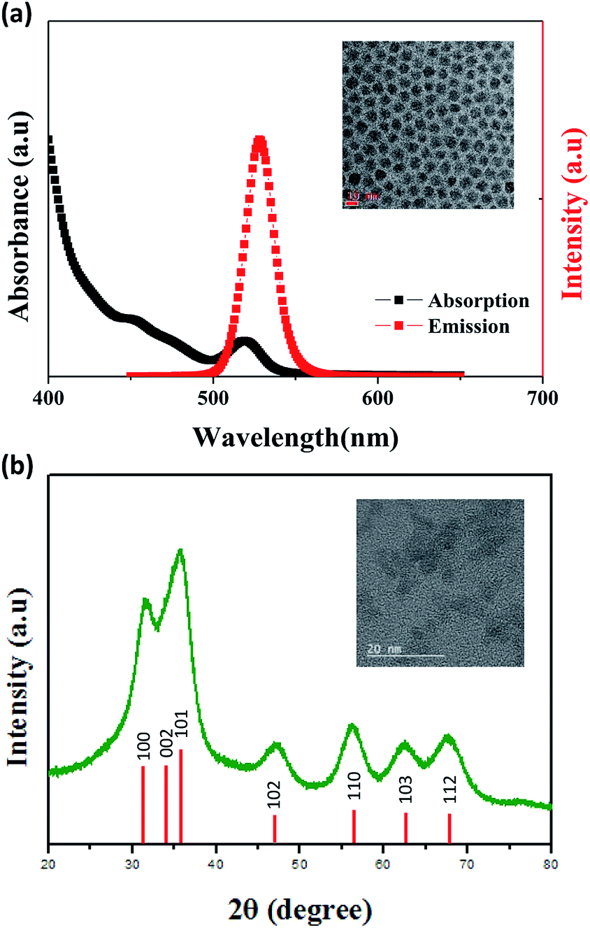 | ||
| Fig. 2 (a) The absorption and PL spectra of green QDs in hexane/octane. (inset) TEM image of QDs, (b) X-ray diffraction pattern of ZnO NPs. (inset) TEM image of ZnO NPs. | ||
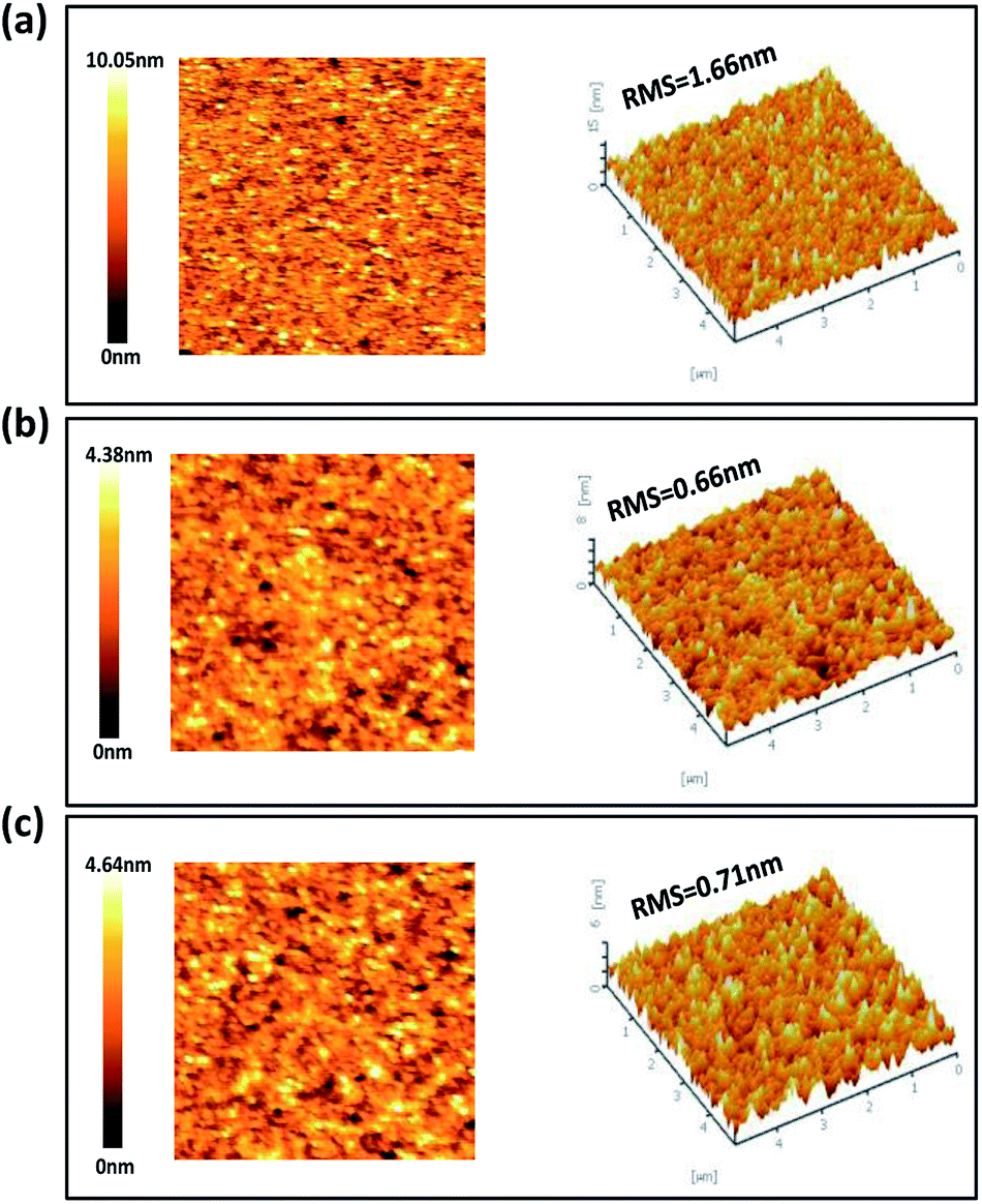
The smooth underlying layer is required for the uniform QDs layers because the efficiency and stability are strongly dependent on the QDs thickness uniformity.30 The surface roughness of ZnO and ZnO/Al2O3 films is shown in Fig. 3. The deposition of the Al2O3 layer on ZnO NPs via the ALD process reduced the root-mean squared (RMS) surface roughness to 0.66 nm of 1 nm Al2O3 layer and 0.71 nm of 2 nm Al2O3 layer from 1.66 nm without the Al2O3 layer. It has been demonstrated that Al2O3 could be deposited well on the ZnO NP surface and the reduction of RMS roughness is attributed to the filling of a valley in the ZnO thin film by the Al2O3 interlayer.29 Smooth surface morphology of the ETL by the Al2O3 interlayer enables uniform QD thin film deposition and low leakage current in QLEDs, which is critical to improve device performance.23 We also measured PL spectra to investigate the effect of Al2O3 interlayer on non-radiative electron transfer induced by ZnO NPs as shown in Fig. S5.†14,35,36 The Al2O3 interlayer contributed to preserve fluorescence of QDs by preventing non-radiative electron transfer. The Al2O3 interlayer serves not only as the electron blocking layer suppressing electron injection but also as a buffer layer preventing electron transfer.
 | ||
| Fig. 3 Surface roughness of (a) ZnO, (b) ZnO/Al2O3 (1 nm), and (c) ZnO/Al2O3 (2 nm). | ||
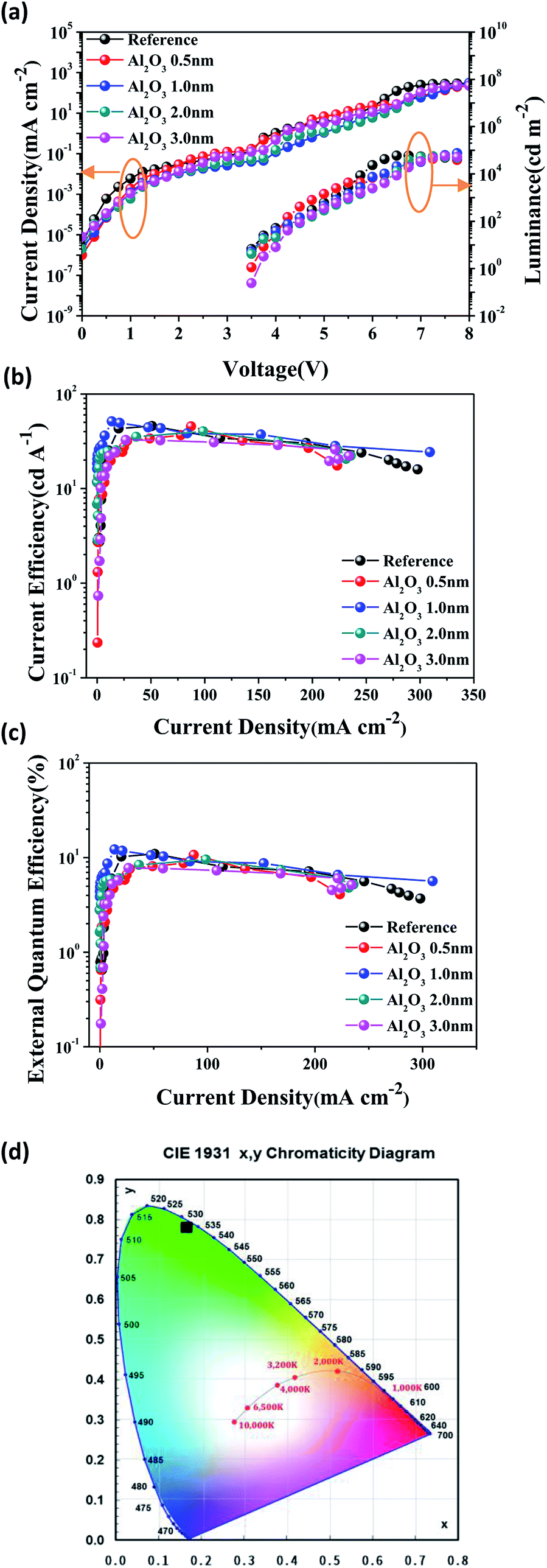
The electrical and optical properties of inverted QLEDs depending on the thickness of the Al2O3 interlayer (from 0 to 3.0 nm) are shown in Fig. 4. The current density of QLEDs was reduced as the thickness of the Al2O3 interlayer increased, and the reduction of the current density was particularly prominent before a turn-on voltage (<3.5 V). The turn-on voltage and luminance for the device without the Al2O3 interlayer are virtually the same as for the device with the Al2O3 interlayer, whereas the current density is much higher as shown in Fig. 4a. The current efficiency and EQE with the 1.0 nm Al2O3 interlayer show the highest enhancement values compared to those without Al2O3 interlayer as shown in Fig. 4b and c and the device performances summarized in Table 1. It demonstrates that the Al2O3 interlayer suppress excessive electron injection due to its insulating property and that charge injection is balanced in the device with the 1.0 nm Al2O3 interlayer. On the other hand, the performance with a 0.5 nm thick Al2O3 interlayer is nearly identical to that without the Al2O3 interlayer. It demonstrates that the very thin interlayer hardly interferes with the injection of electrons, even though it is an insulating materials. We are also worth noting that the device performances drastically decreases and the turn-on voltage is delayed when the thickness of the Al2O3 interlayer is above 3.0 nm (Fig. S6†). The reduction of device performance and the delay of the turn-on voltage are evident when Al2O3 interlayer is thicker than 5.0 nm (Fig. S7†) and this phenomena can be explained with tunneling effect.31 The Al2O3 interlayer acts as a tunneling barrier, and the tunneling current decreases exponentially as the thickness of the barrier layer increases.32 However, in our results, the thickness dependence of the current does not seem to be exponential and this might because the Al2O3 film on the ZnO NP film was not continuous film. The optimum thickness of Al2O3 interlayer is found to be 1.0 nm and the 1.1-fold improved current efficiency of 51.2 cd A−1 and EQE of 12.2% (average: 9.6 ± 1.3) were achieved by suppressing excessive electron injection. The EQEs of the 20 unencapsulated QLEDs with the 1.0 nm Al2O3 interlayer are summarized in histogram (Fig. S8†). The device with Al2O3 interlayer emit deep green light with the Commission International de l'Eclairage (CIE) coordinates of (0.16, 0.78) as shown in Fig. 4d.
 | ||
| Fig. 4 Optical and electrical properties of QLEDs (a) current density–voltage and luminance–voltage, (b) current efficiency–current density, (c) external quantum efficiency–current density and (d) CIE coordinate of the QLEDs with the 1.0 nm Al2O3 interlayer. | ||
| Max. luminance (cd m−2) | Max. current efficiency (cd A−1) | Max. EQE (%) | |
|---|---|---|---|
| Reference | 59![[thin space (1/6-em)]](https://www.rsc.org/images/entities/char_2009.gif) 000 000 |
45.8 | 10.9 |
| Al2O3 (0.5 nm) | 52800 |
45.3 | 10.7 |
| Al2O3 (1.0 nm) | 75100 |
51.2 | 12.2 |
| Al2O3 (2.0 nm) | 57600 |
40.2 | 9.5 |
| Al2O3 (3.0 nm) | 57100 |
32.6 | 7.8 |
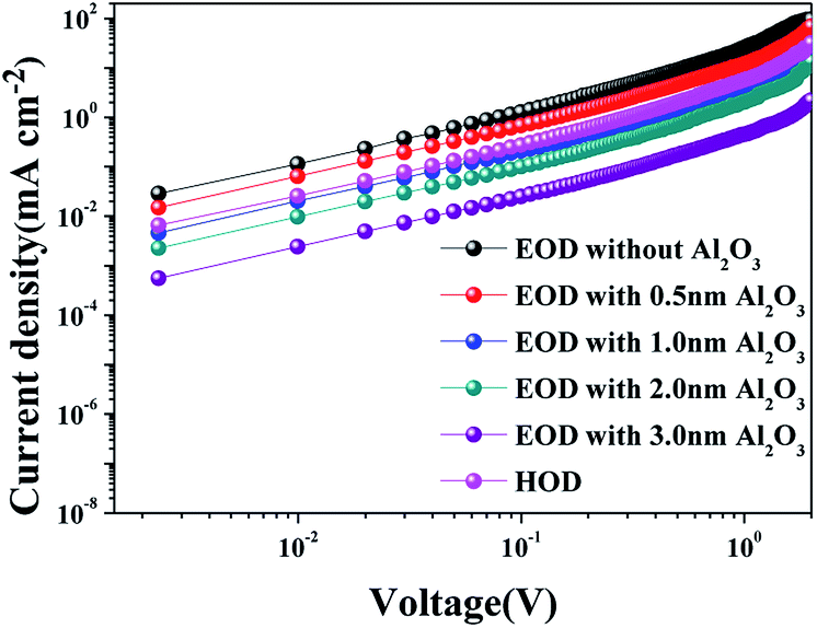
The charge balance depending on the thickness of the Al2O3 interlayer was investigated by electron only (ITO/ZnO/QD/ZnO/Al) and hole only (ITO/poly-TPD/QD/poly-TPD/MoOx/Al) devices as shown in Fig. 5. The significantly higher current density is observed in the electron only device without the Al2O3 interlayer than that of hole only device and this indicates the significant imbalance of charge injection.34 The current density of the electron only device with the 0.5 nm Al2O3 interlayer is similar to that of the electron only device without the Al2O3 interlayer. The current density decreases with the increase as Al2O3 interlayer thickness increases, and the current density of the electron only device is similar to that of hole only device with the 1.0 nm Al2O3 interlayer. Charge injection with the 1.0 nm Al2O3 interlayer is well balanced and thinner Al2O3 interlayer hardly affects with electron injection. We also analyzed impedance to elucidate thickness effect of the Al2O3 interlayer further from electrochemical impedance spectroscopy (EIS). The amplitude of impedance increases drastically and phase angles are in the range of 80–90° when the thickness of the Al2O3 interlayer is above 2.0 nm (Fig. S9†). Both the impedance and the phase angle responses indicate the drastic increase in resistance and capacitance with the Al2O3 interlayer thicker than 1.0 nm resulting in the significant suppression of charge injection.
 | ||
| Fig. 5 Current densities of electron only device (EOD, ITO/ZnO/QD/ZnO/Al) without and with Al2O3 interlayers, and current density of hole only device (HOD, ITO/poly-TPD/QD/poly-TPD/MoOx/Al). | ||
The effect of applied voltage on EL spectra was investigated with and without the Al2O3 interlayer as shown in Fig. 6. The EL emission of the device with the Al2O3 interlayer remains unchanged with different applied voltages, whereas the EL emission of the device without the Al2O3 interlayer shifts to lower energy. The shift of EL emission peak at different applied voltages reflects the operational stability of QLEDs, and this is known to be related to QDs degradation caused by joule heating originated from Auger recombination in QLEDs.19,37 The peak shift of EL emission indicates that the insulating Al2O3 interlayer also improves the stability of EL emission by suppressing the joule heating.
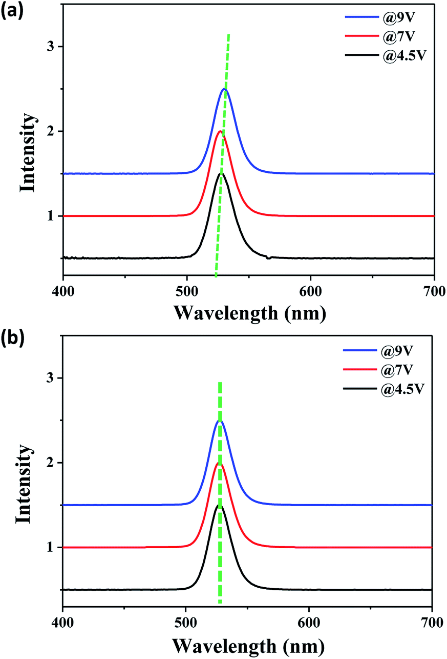 | ||
| Fig. 6 EL spectra of the devices (a) without and (b) with the Al2O3 interlayer depending on applied voltages. | ||
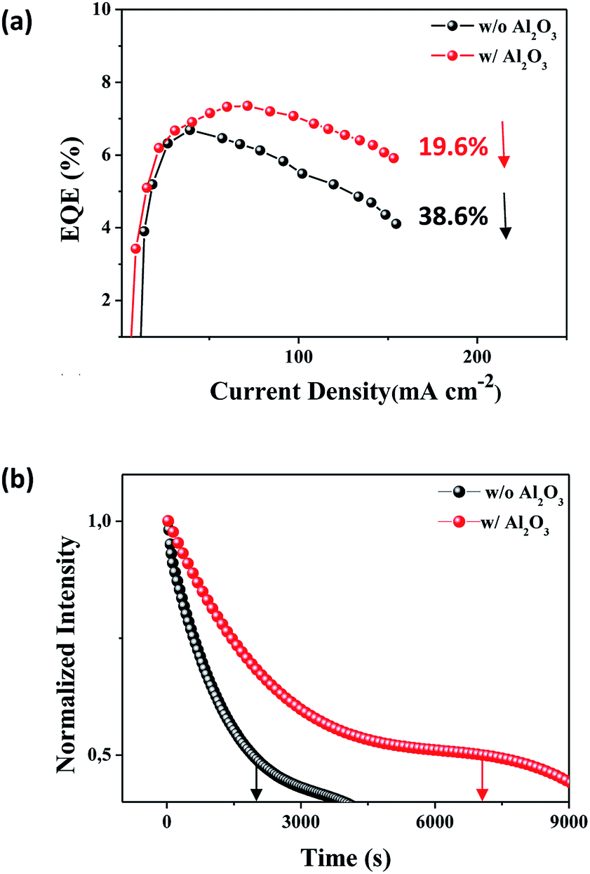
We investigated efficiency roll-off that can be an indicator of the exciton quenching by Auger recombination on the QLEDs as shown in Fig. 7a.19 The efficiency roll-off of 38.6% at 150 mA cm−2 was observed without the Al2O3 interlayer and 19.6% observed with the Al2O3 interlayer. The EQE with the Al2O3 interlayer was also maintained higher than that without Al2O3 interlayer throughout the entire experimental current density range. Device lifetime was monitored as shown in Fig. 7b and also improved by the Al2O3 interlayer since the exciton quenching, such as Auger recombination, was suppressed by interfering with excess electron injection. The devices were tested with a constant driving current density (10 mA cm−2) without encapsulation for the lifetime measurement. The lifetime is defined here with the time for the initial luminance to reduce to half. Initial luminance was 2600 and 1750 cd m−2 with and without the Al2O3 interlayer, respectively. The device with the Al2O3 interlayer shows the device half lifetime of 7070 s, which improved by 3-fold as compared to 2030 s for the device without the Al2O3 interlayer. The half lifetime can be converted into the lifetime at 100 cd m−2 with the following relation.38
| Ln0T50 = constant (n = 1.5) | (1) |
 | ||
| Fig. 7 (a) Efficiency roll-off and (b) device lifetime of QLEDs without and with Al2O3 interlayer. | ||
At luminance of 100 cd m−2, the device lifetime is about 42 h and 260 h for the devices without and with Al2O3 interlayer, respectively. The device lifetime with the Al2O3 interlayer is improved about 6 times than the device without the Al2O3 interlayer.
Conclusions
We deposited a 1.0 nm thick Al2O3 interlayer by an ALD process between EML and ETL of inverted QLED. The ALD process enables precise thickness control in the atomic scale. The 1.0 nm thick Al2O3 interlayer improves the charge balance in the device and the device with the interlayer exhibited device performances of 51.2 cd A−1 in current efficiency and 12.2% in EQE. The efficiency roll-off was suppressed from 38.6% to 19.6% at current density up to 150 mA cm−2 and the device lifetime increased about 6 times than the device without Al2O3 interlayer. The Al2O3 interlayer as a tunneling barrier reduces leakage current of the device and improves radiative recombination in the EML by suppressing Auger recombination and non-radiative electron transfer induced by ZnO NPs. This work demonstrates for the first time within our knowledge in the inverted QLEDs that the Al2O3 interlayer is a promising candidate for charge control and paves a reliable way for fabricating the efficient and stable devices.Conflicts of interest
There are no conflicts to declare.Acknowledgements
This research was supported by the Global Frontier R&D Program on Center for Multiscale Energy System funded by the National Research Foundation under the Ministry of Science, ICT & Future Planning, Korea (2012M3A6A7054855). This work was supported by the National Research Foundation of Korea (NRF) grant funded by the Korea government (MSIT) (2018R1A2A3074950).Notes and references
- P. O. Anikeeva, J. E. Halpert, M. G. Bawendi and V. Bulovic, Nano Lett., 2009, 9, 2532 CrossRef CAS PubMed.
- J. Zhao, J. A. Bardecker, A. M. Munro, M. S. Liu, Y. Niu, I. K. Ding, J. Luo, B. Chen, A. K. Y. Jen and D. S. Ginger, Nano Lett., 2006, 6, 463–467 CrossRef CAS PubMed.
- D. V. Talapin, J. Lee, M. V. Kovalenko and E. V. Shevchenko, Chem. Rev., 2010, 110, 389–458 CrossRef CAS PubMed.
- L. Qian, Y. Zheng, J. Xue and P. H. Holloway, Nat. Photonics, 2011, 5, 543–548 CrossRef CAS.
- H. J. Yun, T. Paik, M. E. Edley, J. B. Baxter and C. B. Murray, ACS Appl. Mater. Interfaces, 2014, 6, 3721–3728 CrossRef CAS PubMed.
- H. Y. Yang, Y. Fu, M. S. Jang, Y. Li, J. H. Lee, H. Chae and D. S. Lee, ACS Appl. Mater. Interfaces, 2016, 8, 35021–35032 CrossRef CAS PubMed.
- J. W. Stouwdam and R. A. J. Janssen, J. Mater. Chem., 2008, 18, 1889–1894 RSC.
- N. Kim, W. Na, W. Yin, H. Jin, T. K. Ahn, S. M. Cho and H. Chae, J. Mater. Chem. C, 2016, 4, 2457–2462 RSC.
- B. Mashford, M. Stevenson, Z. Popovic, C. Hamilton, Z. Zhou, C. Breen, J. Steckel, V. Bulovic, M. Bawendi, S. Coe-Sullivan and P. T. Kazlas, Nat. Photonics, 2013, 7, 407–412 CrossRef CAS.
- Y. Fu, D. Kim, H. Moon, H. Yang and H. Chae, J. Mater. Chem. C, 2017, 5, 522 RSC.
- J. Pan, J. Chen, Q. Huang, Q. Khan, X. Liu, Z. Tao, Z. Zhang, W. Lei and A. Nathan, ACS Photonics, 2016, 3, 215–222 CrossRef CAS.
- H. M. Kim, D. Geng, J. Kim, E. Hwang and J. Jang, ACS Appl. Mater. Interfaces, 2016, 8, 28727–28736 CrossRef CAS PubMed.
- G. Zaiats, S. Ikeda, S. Kinge and P. V. Kamat, ACS Appl. Mater. Interfaces, 2017, 9, 30741–30745 CrossRef CAS PubMed.
- X. Dai, Z. Zhang, Y. Jin, Y. Niu, H. Cao, X. Liang, X. Chen, J. Wang and X. Peng, Nature, 2014, 515, 96–99 CrossRef CAS PubMed.
- D. Kim, Y. Fu, S. Kim, W. Lee, K. H. Lee, H. K. Chung, H. J. Lee, H. Yang and H. Chae, ACS Nano, 2017, 11, 1982–1990 CrossRef CAS PubMed.
- K. H. Lee, J. H. Lee, W. S. Song, H. Ko, C. Lee, J. H. Lee and H. Yang, ACS Nano, 2013, 7, 7295–7302 CrossRef CAS PubMed.
- Q. Lin, L. Wang, Z. Li, H. Shen, L. Guo, Y. Kuang, H. Wang and L. S. Li, ACS Photonics, 2018, 5, 939–946 CrossRef CAS.
- V. I. Klimov, A. A. Mikhailovsky, D. W. McBranch, C. A. Leatherdale and M. G. Bawendi, Science, 2000, 287, 1011–1013 CrossRef CAS PubMed.
- W. K. Bae, Y. S. Park, J. Lim, D. Lee, L. A. Padilha, H. McDaniel, I. Robel, C. Lee, J. M. Pietryga and V. I. Klimov, Nat. Commun., 2013, 7, 9019–9026 Search PubMed.
- W. K. Bae, S. Brovelli and V. I. Klimov, MRS Bull., 2013, 38, 721–730 CrossRef.
- J. Kwak, J. Lim, M. Park, S. Lee, K. Char and C. Lee, Nano Lett., 2015, 15, 3793–3799 CrossRef CAS PubMed.
- P. Rastogi, F. Palazon, M. Prato, F. Di Stasio and R. Krahne, ACS Appl. Mater. Interfaces, 2018, 10, 5665–5672 CrossRef CAS PubMed.
- A. Castelli, F. Meinardi, M. Pasini, F. Galeotti, V. Pinchetti, M. Lorenzon, L. Manna, I. Moreels, U. Giovanella and S. Brovelli, Nano Lett., 2015, 15, 5455 CrossRef CAS PubMed.
- K. Ding, H. Chen, L. Fan, B. Wang, Z. Huang, S. Zhuang, B. Hu and L. Wang, ACS Appl. Mater. Interfaces, 2017, 9, 20231–20238 CrossRef CAS PubMed.
- H. Zhang, N. Sui, X. Chi, Y. Wang, Q. Liu, H. Zhang and W. Ji, ACS Appl. Mater. Interfaces, 2016, 8, 31385–31391 CrossRef CAS PubMed.
- Y. Q. Yang, Y. Duan, P. Chen, F. B. Sun, Y. H. Duan, X. Wang and D. J. Yang, J. Phys. Chem. C, 2013, 117, 20308–20312 CrossRef CAS.
- Y. Duan, F. Sun, Y. Yang, P. Chen, D. Yang, Y. Duan and X. Wang, ACS Appl. Mater. Interfaces, 2014, 6, 3799–3804 CrossRef CAS PubMed.
- Y. Fu, D. Kim, W. Jiang, W. Yin, T. K. Ahn and H. Chae, RSC Adv., 2017, 7, 40866–40872 RSC.
- J.-H. Choi, J. Kim, S. J. Oh, D. Kim, Y.-H. Kim, H. Chae and H. Kim, Met. Mater. Int., 2016, 22, 723–729 CrossRef CAS.
- H. M. Kim, J. H. Youn, G. J. Seo and J. Jang, J. Mater. Chem. C, 2013, 1, 1567–1573 RSC.
- H. A. Al Attar and A. P. Monkman, Adv. Funct. Mater., 2006, 16, 2231–2242 CrossRef CAS.
- Y. E. Kim, H. Park and J. J. Kim, Appl. Phys. Lett., 1996, 69, 599–601 CrossRef CAS.
- Y. Zhou, C. Fuentes-Hernandez, J. Shim, J. Meyer, A. J. Giordano, H. Li, P. Winget, T. Papadopoulos, H. Cheun, J. Kim, M. Fenoll, A. Dindar, W. Haske, E. Najafabadi, T. M. Khan, H. Sojoudi, S. Barlow, S. Graham, J. L. Bredas, S. R. Marder, A. Kahn and B. Kippelen, Science, 2012, 336, 327–332 CrossRef CAS PubMed.
- J. Li, Z. Liang, Q. Su, H. Jin, K. Wang, G. Xu and X. Xu, ACS Appl. Mater. Interfaces, 2018, 10, 3865–3873 CrossRef CAS PubMed.
- K. Tvrdy, P. A. Frantsuzov and P. V. Kamat, Proc. Natl. Acad. Sci. U. S. A., 2011, 108, 29–34 CrossRef CAS PubMed.
- V. Wood, M. J. Panzer, L. E. Halpert, J. M. Caruge, M. G. Bawendi and V. Bulovic, ACS Nano, 2009, 3, 3581–3586 CrossRef CAS PubMed.
- S. Shendre, V. K. Sharma, C. Dang and H. V. Demir, ACS Photonics, 2018, 5, 480–486 CrossRef CAS.
- P. Wellmann, M. Hofmann, O. Zeika, A. Werner, J. Birnstock, R. Meerheim, G. He, K. Walzer, M. Pfeiffer and K. Leo, J. Soc. Inf. Disp, 2005, 13, 393–397 CrossRef CAS.
Footnote |
| † Electronic supplementary information (ESI) available. See DOI: 10.1039/c9ra00145j |
| This journal is © The Royal Society of Chemistry 2019 |