
 Open Access Article
 This Open Access Article is licensed under a Creative Commons Attribution-Non Commercial 3.0 Unported Licence
The application of a non-doped composite hole transport layer of [MoO3/CBP]n with multi-periodic structure for high power efficiency organic light-emitting diodes
Zhixiang Gao†
 *ab,
Zilong Feng†a,
Weihua Chenc,
Wenshan Qu*b,
Wei Aoc,
Tingting Yangb,
Jiangang Lib and
Feng Gaoc
*ab,
Zilong Feng†a,
Weihua Chenc,
Wenshan Qu*b,
Wei Aoc,
Tingting Yangb,
Jiangang Lib and
Feng Gaoc
aSchool of Architecture, Tianjin University, Tianjin 300072, P. R. China. E-mail: gao_zhixiang@126.com
bShanxi Province Key Laboratory of Microstructure Functional Materials, Institute of Solid State Physics, Shanxi Datong University, Datong 037009, P. R. China. E-mail: wenshanqu@126.com
cKunShan Govisionox Optoelectronics Co., Ltd., Soochow 215000, China
First published on 8th February 2019
Abstract
A non-doped multi-periodic structure of composite hole transport layer of [MoO3/CBP]n was applied to organic light-emitting diodes. All devices with such hole transport layers showed low turn-on voltage of about 3 V, ultra-high luminance of >110![[thin space (1/6-em)]](https://www.rsc.org/images/entities/char_2009.gif) 000 cd m−2, high current efficiency of >50 cd A−1, and high EQE of more than 15%. The optimized device exhibited power efficiency increase of 66% and 18% relative to the single periodic and doped structure OLEDs. The achievement of the reduced driving voltage and improved power efficiency can be attributed to the significantly enhanced hole injection and transport induced by the multi-periodic structure of composite hole transport layer, which was demonstrated via a series of hole-only devices. For improved hole injection and transport mechanism, we also provided a detailed discussion in combination with atomic force microscopy measurements.
000 cd m−2, high current efficiency of >50 cd A−1, and high EQE of more than 15%. The optimized device exhibited power efficiency increase of 66% and 18% relative to the single periodic and doped structure OLEDs. The achievement of the reduced driving voltage and improved power efficiency can be attributed to the significantly enhanced hole injection and transport induced by the multi-periodic structure of composite hole transport layer, which was demonstrated via a series of hole-only devices. For improved hole injection and transport mechanism, we also provided a detailed discussion in combination with atomic force microscopy measurements.
1. Introduction
Organic light-emitting diodes (OLEDs) have received increasing attention in the past 30 years due to their huge potential applications in flat-display and solid-lighting fields, and great progress has been made both in academia and industry.1–6 For example, many monochrome and white OLEDs exhibiting external quantum efficiency (EQE) beyond the theoretical limit (5% for fluorescent OLEDs and 20% for phosphorescent OLEDs) have been widely reported in the literature,7–10 and OLED flat-displays are already being used in many small electronic products such as cell phones. However, the power efficiency, rather than EQE, is the key parameter, which is used to evaluate device performance for commercialization applications.8,11,12 In order to improve power efficiency, the driving voltage of the device should be as small as possible, where the anode buffer layer or hole injection layer combining with the hole transport layer (HTL) to form the composite hole transport layer (C-HTL) is very important. C-HTL can comprise inorganic–organic materials,13,14 organic–organic materials,15 doped single functional layers16,17 or non-doped bilayer structures.18–20 For example, C-HTLs of WoO3/CBP,19 HAT-CN/TAPC,15 CBP:x% MoO3,16 and MoO3/4p-NPD20 have been applied in OLEDs, and the devices with these C-HTLs have exhibited markedly improved power efficiency.13–20Among the C-HTLs formed from different materials and structures, we focused on the application of transition metal oxides (TMOs), which are very important materials for electrodes or for charge generation/recombination due to the high work function, excellent semiconducting properties and good transparency. Among various TMOs such as MoO3, WoO3 and V2O5, MoO3 is the most common material used to reduce the energy offset between anode and HTL in OLEDs; it further reduces the hole injection energy barrier and improves hole injection.21–23 These contribute to a reduced driving voltage and improved power efficiency. In general, MoO3 is deposited as a thin layer (2–5 nm) to form the bilayer C-HTL structure of MoO3/HTL. Except for the above-mentioned non-doped structures, C-HTLs containing doped MoO3 in HTL (NPB, TCTA and CBP) also provide an efficient method to improve device performance.18–20 However, such C-HTLs containing doped MoO3 with co-evaporated MoO3 and HTL suffer from some problems. For example, it is very difficult to accurately control the concentration of MoO3 and cross-contamination inevitably occurs between different deposition sources during the co-deposition process in a vacuum chamber. More seriously, excessive aggregation of MoO3 in HTL may become harmful to device. For non-doped C-HTLs, there are few reports about the multi-periodic structure, which is an important structure type in photoelectrical devices. Therefore, we aimed to fabricate multi-periodic C-HTLs by employing MoO3 thin layers to research the influence on device performance.
In this manuscript, we utilized MoO3 and 4,4-bis(9-carbazolyl)-bisphenyl (CBP) to form the non-doped multi-periodic C-HTL structure of [MoO3/CBP]n and we studied the effect on device efficiency. We found that the device with a 3-periodic structure of C-HTLs exhibited significantly reduced driving voltage and improved power efficiency. In order to reveal the reason for the achievement of high power efficiency, the hole injection and transport mechanisms in these OLEDs with multi-periodic C-HTL structure of [MoO3/CBP]n were studied by atomic force microscopy (AFM) and single carrier device.
2. Experimental section
2.1 Device fabrication
All materials involved were procured commercially and used without further purification. Indium tin oxide (ITO) substrates with a square resistance of 15 Ω were ultrasonically washed in acetone, deionized water and acetone in sequence to keep them completely clean. After that, ITO substrates were irradiated under ultraviolet light for 15 minutes to improve the work function before loading them into a vacuum chamber. The OLEDs were then fabricated by thermal evaporation method in high vacuum level (less than 3 × 10⁻⁴ Pa) on top of ITO substrates, with the effective area of 3 mm × 3 mm. The film thicknesses and the corresponding deposition rates were controlled by calibrated crystal quartz sensors. Deposition rates of functional organic layers, MoO3, LiF, and Al were about 1 Å s−1, 0.5 Å s−1, 0.5 Å s−1, and 3–6 Å s−1, respectively.2.2 Characterization
The current–voltage–luminance curves and electroluminescence (EL) spectra of OLEDs were measured on a measuring platform integrated with a Keithley 2400 source meter, BM-7A luminance colorimeter and PR655 spectra scan spectrometer. External quantum efficiency (EQE) was calculated from the current density–voltage–luminance curve and EL spectra data. The AFM images were obtained by measuring the films prepared on clean ITO substrates with SPA-300HV Atomic Force Microscopy from NSK Ltd. All devices were measured immediately at room temperature after fabrication without encapsulation in laboratory environment.3. Results and discussion
As shown in Fig. 1a, OLEDs with a non-doped multi-periodic C-HTL adopt the structure as follows: ITO/C-HTLs (40 nm)/TCTA (10 nm)/CBP:6 wt% Ir(ppy)3 (30 nm)/TPBi (40 nm)/LiF (1 nm)/Al (100 nm). The C-HTL structures include a single periodic reference device of [MoO3 (3 nm)/CBP (37 nm)] for D-1, two periodic devices of [MoO3 (3 nm)/CBP (17 nm)]2 for D-2 and three periodic devices of [MoO3 (3 nm)/CBP (10.3 nm)]3 for D-3. Among these devices, the total thickness of C-HTLs remained constant at 40 nm. Other functional layers of the OLEDs include 4,4′,4′′-tris(9-carbazolyl)triphenylamine (TCTA) as the electron and exciton blocking layer, CBP:6 wt% tris(2-phenylpyridine) iridium(III) (Ir(ppy)3) as the emitting layer, 1,3,5-tris(1-phenyl-1H-benzimidazol-2-yl)benzene (TPBi) as the electron transport layer and LiF/Al as the composite cathode.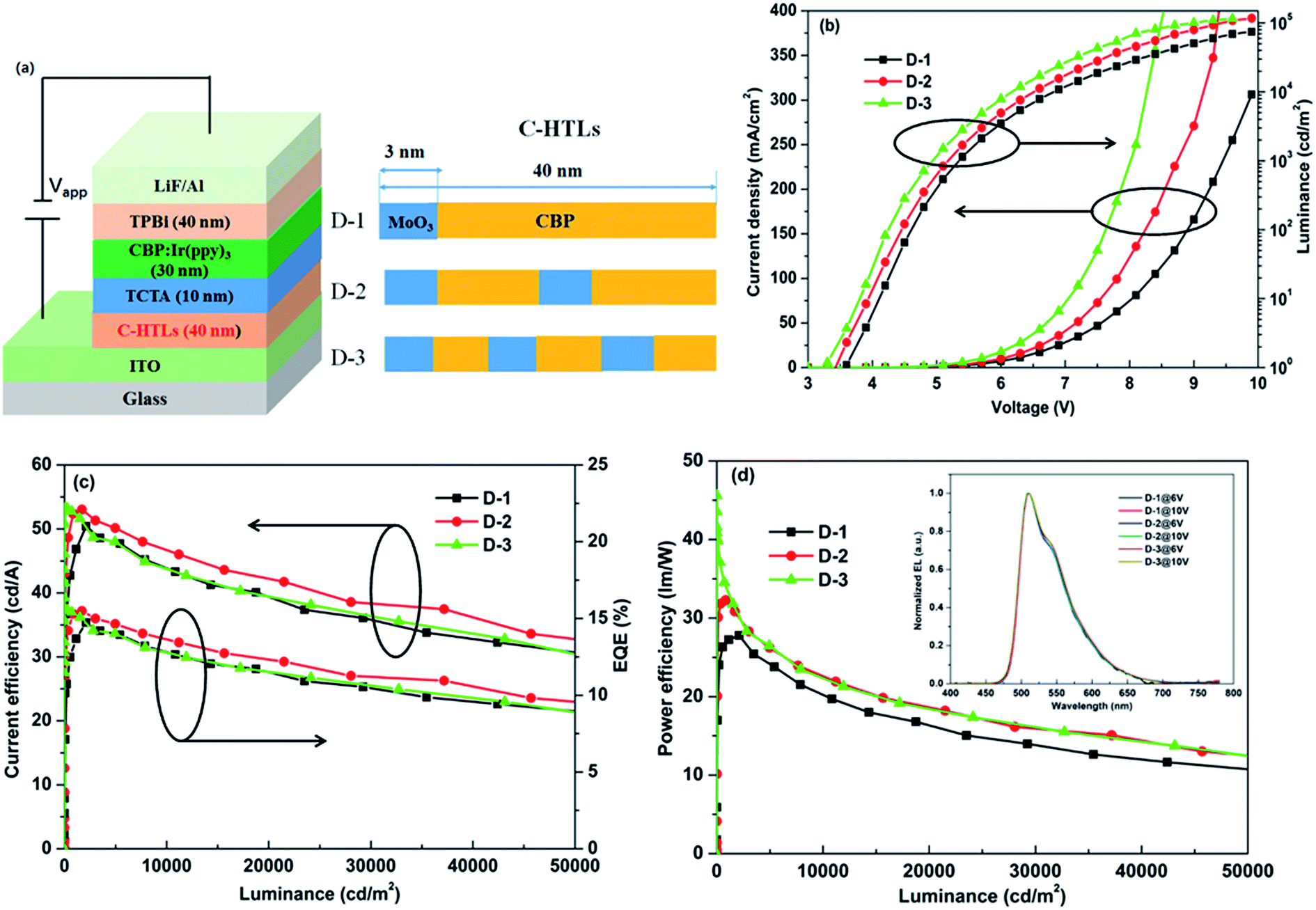 | ||
| Fig. 1 Device structure and EL performances. (a) Device structure. (b) Current density–voltage–luminance curves. (c) Current efficiency–luminance–EQE curves. (d) Power efficiency–luminance curves. Inset is the EL spectra under different voltages. | ||
Fig. 1b exhibits the current density–voltage–luminance curves of devices D-1, D-2 and D-3. We can see that with the increase in periodic number of [MoO3/CBP]n from 1 to 3, the corresponding devices showed significantly enhanced current density and luminance and reduced turn-on voltage. All three devices achieved ultra-high emission luminance of >110000 cd m−2. Among all three devices, device D-3 exhibited the lowest turn-on voltage of 3.2 V and achieved the highest current density and luminance at the same driving voltage. This was because the MoO3 thin layer between the ITO anode and CBP helped the formation of ohmic contact and dramatically decreased the hole injection barrier. The injection barrier could reduce from 1 eV to 0.1–0.2 eV.24,25 In addition, the MoO3 layers in CBP to form non-doped periodic structure of C-HTLs could further improve the transport of holes by increasing the mobility and carrier density. The great enhancement in current density with increased periodic number demonstrated better conductivity of non-doped 3-periodic structure of C-HTLs, which indicated optimized hole injection and transport.26–30
The current efficiency–luminance–EQE and power efficiency–luminance curves are shown in Fig. 1c and d, respectively. It can be seen that the maximum current efficiency and EQE values of the three devices are similar, and they are maintained in the ranges of 50–53 cd A−1 and 14.7–15.6%, respectively. However, the maximum power efficiencies of the three devices were very different: 27, 32 and 45 lm W−1 for D-1, D-2, and D-3, respectively. This indicated that the 3-periodic C-HTL structure OLED (device D-3) achieved the highest power efficiency, and the improved ratio reached 66% relative to that of the single periodic reference device (device D-1). The low turn-on voltage is the main reason for the achievement of high power efficiency, which results from the improved hole injection and transport ability. The improved hole injection and transport led to a more balanced recombination with electrons for the 3-periodic C-HTL structure device. The EL spectra for devices D-1, D-2 and D-3 at 6 V and 10 V are explored and shown in the inset of Fig. 1d. It can be seen that the spectra for the three devices remain the same with an emission peak at typical 512 nm even with the introduction of the periodic structure in C-HTLs.31,32 In addition, no other emissions from the transport layer were observed; this indicated that although hole injection increased with more periodic number, the electron and hole could also be well confined in the emitting layer (EML) due to the suitable energy level and high exciton energy of TCTA (0.3 eV for electron, T1 = 2.76 eV) and TPBi (0.3 eV for hole, T1 = 2.74 eV).33–35 This demonstrated that C-HTL does not influence the recombination zone and the formation of Ir(ppy)3 excitons. The application of the non-doped multi-periodic C-HTL structure is helpful for simplifying the fabrication process and improving the repeatability compared to the application of a doped structure. If the total thickness of HTL is more than 40 nm, more periodic number (n > 3) can further improve the efficiency; in contrast, it would increase the complexity of the devices and also breach our original design for the non-doped C-HTLs.
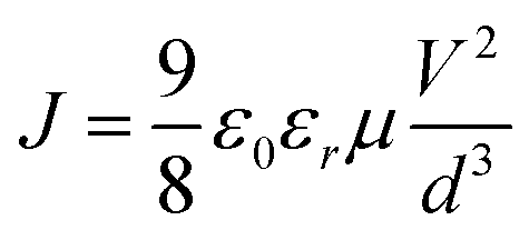
In order to identify the hole transport ability of the non-doped multi-periodic structure of C-HTL, a hole-only device was fabricated (the inset of Fig. 2) with the structure of ITO/C-HTLs (40 nm)/TCTA (20 nm)/Al; the C-HTLs were consistent with the C-HTLs of D-1–D-3, and the hole-only devices were defined as H-1–H-3, respectively. In the hole-only devices, TCTA played the role of the electron blocking layer to block electron injection from the Al cathode. Fig. 2 shows the relationship curves of the current density to voltage for H-1–H-3. The current density increased with the periodic number (n), which indicated improvement in hole transport ability. If the J–V (current density–voltage) data of each device fit formula (1) according to the space charge limited current model (SCLC), the mobility (μ) of each C-HTL can be approximately obtained.36,37 Given that the voltage and thickness of an organic layer (d) are kept constant, the mobility of C-HTL can be improved dramatically with increasing periodic number. It can be inferred that MoO3 located between CBP in the periodic structure has a p-type doping effect just as that of the homogeneous mixing method to enhance the mobility and conductivity of HTL.
 | (1) |
 | ||
| Fig. 2 The current density–voltage curves of hole-only devices with different periodic C-HTLs. | ||
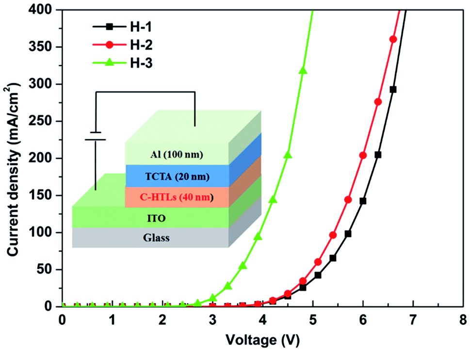
Considering that different structures determine the surface roughness of C-HTL films that may influence the performance of devices, the morphologies of C-HTL films were investigated by AFM. Related root mean squares (RMS) of surface roughness for the periodic structures are given in Fig. 3. It demonstrates that multi-periodic structures show small surface roughness and the change with periodic number (n) is so small that the differences can be neglected (RMS from 1.08 to 1.17 nm for single periodic to 3-periodic). This indicated that the multi-periodic C-HTL structure did not significantly change the surface roughness, which supported efficient hole injection and transport in multi-periodic C-HTLs.
 | ||
| Fig. 3 AFM of three kinds of periodic structure C-HTLs: (a) single periodic; (b) two periodic; (c) three periodic. | ||
The detailed hole injection process from the ITO anode to C-HTLs and the hole transport process are demonstrated in Fig. 4, which are considered from the perspective of energy level alignment. The highest occupied molecular orbital (HOMO) of CBP would rise to the Fermi level,38 which induces energy band bending at the interface between the conduction band bottom of MoO3 and the HOMO of CBP. This can then lead to decrease of the energy barrier for hole injection from ITO to CBP (nearly approaching zero), as seen in Fig. 4a.39,40 Simultaneously, just as suggested in Fig. 4b, MoO3 in the CBP layer would diffuse into both sides driven by thermal activity or a concentration gradient. Since MoO3 exhibits strong electron absorption ability, electrons can transfer easily from the HOMO of CBP to the conduction band bottom of MoO3.41,42 Finally, it is reasonable that the holes would move along the HOMO of the CBP penetrating the MoO3 unit. The improvement in conductivity of C-HTLs and the balanced degree of holes and electrons make the devices composed of [MoO3/CBP]n periodic units accomplish excellent performance: lower injection barrier and driving voltage, higher hole mobility, superior power efficiency and luminance.
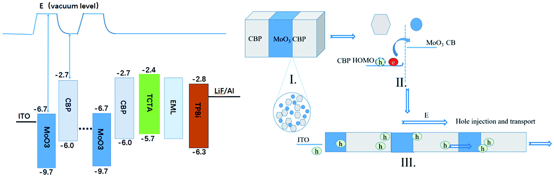 | ||
| Fig. 4 The energy level schematic diagram and hole transport mechanism of the OLEDs with multi-periodic structure C-HTLs. | ||
We also fabricated the doped structure of C-HTL device for comparison with the 3-periodic structure of C-HTL. It was found that the 3-periodic structure of C-HTL device exhibited best device performance. The OLEDs with doped structure C-HTL exhibited ITO/MoO3 (3 nm)/CBP:16% MoO3 (37 nm)/TCTA (10 nm)/CBP:6 wt% Ir(ppy)3 (30 nm)/TPBi (40 nm)/LiF (1 nm)/Al (100 nm), which was defined as E-3. The EL performances of devices D-3 and E-3 including current density, luminance, current efficiency and power efficiency are shown in Fig. 5. They exhibited similar device performances of luminance and current efficiency with maximum luminance of ∼110000 cd m−2 and maximum current efficiency of ∼52 cd A−1. However, the doped structure of C-HTL of device E-3 showed lower maximum power efficiency of 38 lm W−1, which was 45 lm W−1 for D-3. This indicated the multi-periodic structure of C-HTL is better than the traditional doped structure of C-HTL, which was derived from improved hole injection and balanced hole–electron recombination. The summary of EL performances of all OLEDs studied in this paper is given in Table 1.
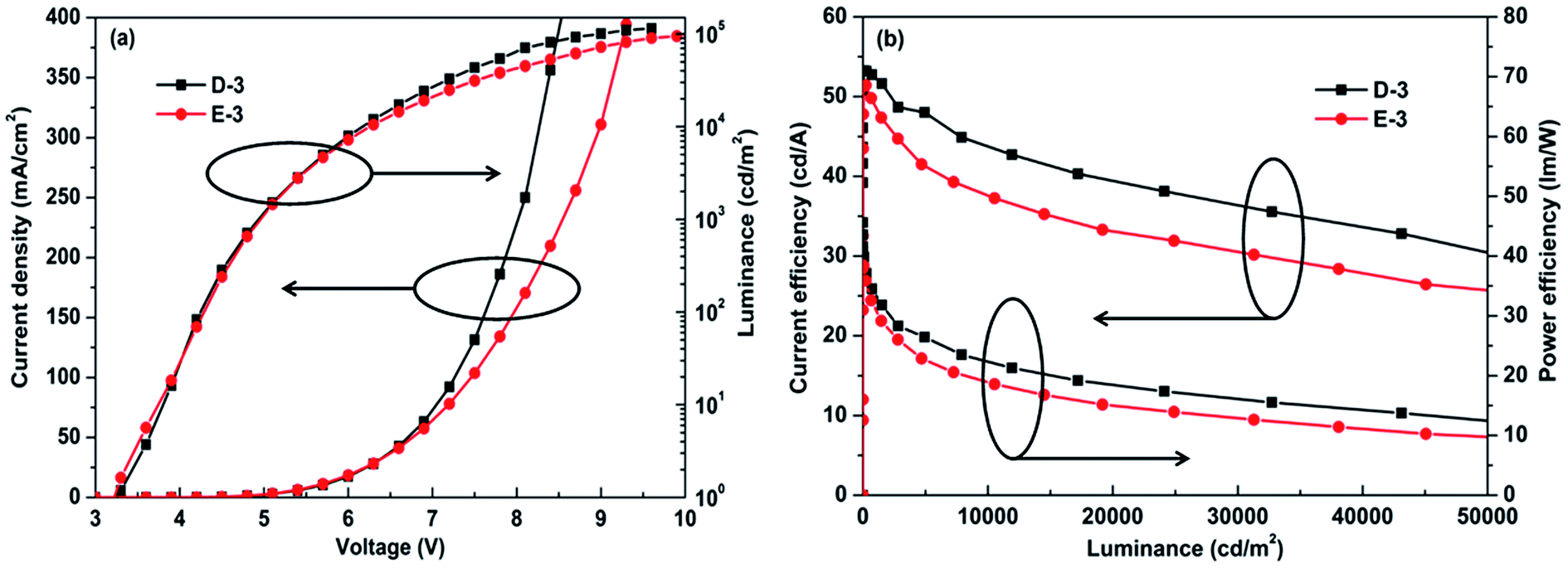 | ||
| Fig. 5 The EL performances of devices D-3 and E-3. (a) Current density–voltage–luminance curves. (b) Current efficiency–luminance–power efficiency curves. | ||
| Vona [V] | Lb [cd m−2] | ηcc [cd A−1 ] | ηpd [lm W−1] | EQEe [%] | |
|---|---|---|---|---|---|
| a Turn-on voltage (at 1 cd m−2).b Maximum luminance.c Current efficiency at maximum and 10000 cd m−2.d Power efficiency at maximum and 10000 cd m−2.e EQE at maximum and 10000 cd m−2. |
|||||
| D-1 | 3.6 | 102000 |
50/44 | 27/20 | 14.7/12.8 |
| D-2 | 3.4 | 117500 |
53/47 | 32/23 | 15.4/13.6 |
| D-3 | 3.2 | 115000 |
53/44 | 45/22 | 15.6/12.8 |
| E-3 | 3.2 | 109000 |
51/38 | 38/19 | 15.0/10.8 |
The AFM results of doped structure of C-HTL films with two different doping ratios (one is consistent with device E-3 and the other conducts the higher doping ratio) are shown in Fig. 6. It can be seen that the doped structure of C-HTL film is coarser and more uneven (RMS = 1.61 nm) as compared to the multi-periodic structure of C-HTL film (RMS = 1.08–1.17 nm), which are shown in Fig. 3. Even RMS reached 4.65 nm at the higher doping concentration of 50%, which indicated that the MoO3 dopants tend to aggregate into different bulk sizes. This suggested that the multi-periodic structure of C-HTLs was more stable and smooth than the doped structure due to a less-aggregated bulk, which led to the better device performance of the periodic structure of C-HTL than the doped structure of C-HTL.
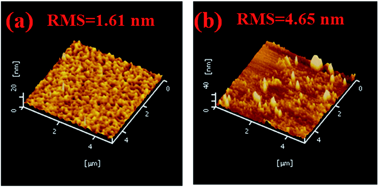 | ||
| Fig. 6 The AFM of C-HTLs film with doping structure. (a) MoO3 (3 nm)/CBP:16% MoO3 (consist with E-3). (b) MoO3 (3 nm)/CBP:50% MoO3 (higher doping ratio). | ||
4. Conclusion
We fabricated Ir(ppy)3-based green phosphorescence OLEDs with non-doped multi-periodic structure of C-HTLs composed of [MoO3/CBP]n (n = 1–3 for D-1–D-3, respectively). All the devices achieved ultra-high luminance of >110000 cd m−2. The device D-3 with a 3-periodic structure exhibited the highest power efficiency of 45 lm W−1, which improved by 66% and 18% ratio as compared to those of D-1 of single periodic reference device and doped structure of C-HTL device, respectively. The better performances of device D-3 were attributed to decreased injection barrier and driving voltage and improved hole transport due to the energy band bending between the Fermi level and the HOMO of CBP. AFM also demonstrated smoother surface morphology of the multi-periodic structure than the doped structure. Therefore, we believe that the periodic structure of C-HTL can replace the doped structure and thus open up a new way to design highly efficient OLEDs.
Conflicts of interest
There are no conflicts to declare.Acknowledgements
This work was financially supported by the National Natural Science Foundation of China (21872088, 11874245), Shanxi Province Science and Technology Key Project (201703D121037-2), Datong City Science and Technology Research Project (2018018).References
- Y. Sun, N. C. Giebink, H. Kanno, B. Ma, M. E. Thompson and S. R. Forrest, Nature, 2006, 440, 908 CrossRef CAS PubMed.
- Y. Miao, K. Wang, B. Zhao, L. Gao, P. Tao, X. Liu, Y. Hao, H. Wang, B. Xu and F. Zhu, Nanophotonics, 2018, 7, 295 CAS.
- S. Reineke, F. Lindner, G. Schwartz, N. Seidler, K. Walzer, B. Lüssem and K. Leo, Nature, 2009, 459, 234 CrossRef CAS PubMed.
- P. Tao, Y. Q. Miao, H. Wang, B. S. Xu and Q. Zhao, Chem. Rec., 2018, 18, 1–32, DOI:10.1002/tcr.201800139.
- Y. Miao, B. Zhao, Z. Gao, H. Shi, P. Tao, Y. Wu, K. Wang, H. Wang, B. Xu and F. Zhu, Org. Electron., 2017, 42, 1 CrossRef CAS.
- N. Li, Y. S. Lau, Y. Miao and F. Zhu, Nanophotonics, 2018, 7, 1981 CAS.
- S. Lee, K. H. Kim, D. Limbach, Y. S. Park and J. J. Kim, Adv. Funct. Mater., 2013, 23, 4105 CrossRef CAS.
- Y. Miao, K. Wang, L. Gao, B. Zhao, H. Wang, F. Zhu, B. Xu and D. Ma, J. Mater. Chem. C, 2018, 6, 8122 RSC.
- C. Lu, M. Jiao, W. K. Lee, C. Chen, W. L. Tsai, C. Lin and C. Wu, Adv. Funct. Mater., 2016, 26, 3250 CrossRef CAS.
- Y. Miao, P. Tao, K. Wang, H. Li, B. Zhao, L. Gao, H. Wang, B. Xu and Q. Zhao, ACS Appl. Mater. Interfaces, 2017, 9, 37873 CrossRef CAS PubMed.
- X. Tang, X. Liu, Y. Yuan, Y. Wang, H. Li, Z. Jiang and L. Liao, ACS Appl. Mater. Interfaces, 2018, 10, 29840 CrossRef CAS PubMed.
- Y. Miao, Z. Gao, H. Wang, H. Jia, X. Liu, B. Xu and B. Wei, Org. Electron., 2015, 23, 199 CrossRef CAS.
- G. L. Frey, K. J. Reynolds, J. A. Barker, N. C. Greenham and R. H. Friend, J. Appl. Phys., 2002, 92, 7556 CrossRef.
- Y. Miao, X. Du, H. Wang, H. Liu, H. Jia, B. Xu, Y. Hao, X. Liu, W. Li and W. Huang, RSC Adv., 2015, 5, 4261 RSC.
- K. S. Lee, I. Lim, S. H. Han and T. W. Kim, Org. Electron., 2014, 15, 343 CrossRef CAS.
- Y. Li, Y. Hao, Z. Yan, H. Liu, H. Wang and B. Xu, Synth. Met., 2013, 164, 12 CrossRef CAS.
- J. Qiu, Z. Wang, M. G. Helander and Z. H. Lu, Appl. Phys. Lett., 2011, 99, 153305 CrossRef.
- Y. Miao, K. Wang, L. Gao, H. Wang, F. Zhu and B. Xu, J. Mater. Chem. C, 2018, 6, 9811 RSC.
- J. Meyer, S. Hamwi, T. Bülow, H. H. Johannes, T. Riedl and W. Kowalsky, Appl. Phys. Lett., 2007, 91, 113506 CrossRef.
- Y. Miao, K. Wang, L. Gao, B. Zhao, Z. Wang, Y. Zhao, A. Zhang, H. Wang, Y. Hao and B. Xu, J. Mater. Chem. C, 2018, 6, 1853 RSC.
- L. Chen, D. Qin, Y. Chen, G. Li, M. Wang and D. Ban, Phys. Status Solidi A, 2013, 210, 1157 CrossRef CAS.
- G. Liu, W. Ji, W. Xie and H. Zhang, Spectrosc. Spectral Anal., 2011, 31, 882 CAS.
- X. Liang, K. Wang, R. Zhang, K. Li, X. Lu, K. Guo, H. Wang, Y. Miao, H. Xu and Z. Wang, Dyes Pigm., 2017, 139, 764 CrossRef CAS.
- J. Meyer, S. Hamwi, M. Kröger, W. Kowalsky, T. Riedl and A. Kahn, Adv. Mater., 2012, 24, 5408 CrossRef CAS PubMed.
- Y. Zhao, J. Zhang, S. Liu, Y. Gao, X. Yang, K. S. Leck, A. P. Abiyasa, Y. Divayana, E. Mutlugun, S. T. Tan, Q. Xiong, H. V. Demir and X. W. Sun, Org. Electron., 2014, 15, 871 CrossRef CAS.
- J. Meyer, P. R. Kidambi, B. C. Bayer, C. Weijtens, A. Kuhn, A. Centeno, A. Pesquera, A. Zurutuza, J. Robertson and S. Hofmann, Sci. Rep., 2014, 4, 5380 CrossRef CAS PubMed.
- X. Jiang, Z. Zhang, J. Cao and W. Zhu, Solid-State Electron., 2008, 52, 952 CrossRef CAS.
- Y. Miao, K. Wang, B. Zhao, L. Gao, J. Xu, H. Wang and B. Xu, RSC Adv., 2017, 7, 49769 RSC.
- Y. Zou, Z. Deng, Z. Lv, Z. Chen, D. Xu, Y. Chen, Y. Yin, H. Du and Y. Wang, J. Lumin., 2010, 130, 959 CrossRef CAS.
- J. Ma, Z. Liang, C. Jin, X. Jiang and Z. Zhang, Solid State Commun., 2009, 149, 214 CrossRef CAS.
- Y. Miao, K. Wang, B. Zhao, L. Gao, Y. Wang, H. Wang, B. Xu and F. Zhu, J. Mater. Chem. C, 2017, 5, 12474 RSC.
- Y. Zhang, G. Zhong and X. Cao, J. Appl. Phys., 2010, 108, 083107 CrossRef.
- S. J. Lee, J. R. Koo, H. W. Lee, S. E. Lee, H. J. Yang, S. S. Yoon, J. Park and Y. K. Kim, Electron. Mater. Lett., 2014, 10, 1127 CrossRef CAS.
- K. M. Hwang, S. E. Lee, S. Lee, H. K. Yoo, H. J. Baek, Y. K. Kim, J. Kim and S. S. Yoon, J. Korean Phys. Soc., 2016, 69, 328 CrossRef CAS.
- Y. Miao, P. Tao, L. Gao, X. Li, L. Wei, S. Liu, H. Wang, B. Xu and Q. Zhao, J. Mater. Chem. C, 2018, 6, 6656 RSC.
- H. Li, L. Duan, D. Zhang and Y. Qiu, J. Phys. Chem. C, 2014, 118, 9990 CrossRef CAS.
- D. S. Pereira, P. L. Santos, J. S. Ward, P. Data, M. Okazaki, Y. Takeda, S. Minakata, M. R. Bryce and A. P. Monkman, Sci. Rep., 2017, 7, 6234 CrossRef PubMed.
- M. Kühn, E. Mankel, A. Köhn, T. Mayer and W. Jaegermann, Phys. Status Solidi B, 2016, 253, 1697 CrossRef.
- T. A. Papadopoulos, J. Meyer, H. Li, Z. Guan, A. Kahn and J. Brédas, Adv. Funct. Mater., 2013, 23, 6091 CrossRef CAS.
- I. Salzmann, G. Heimel, M. Oehzelt, S. Winkler and N. Koch, Acc. Chem. Res., 2016, 49, 370 CrossRef CAS PubMed.
- S. Beck, D. Gerbert, T. Glaser and A. Pucci, J. Phys. Chem. C, 2015, 119, 12545 CrossRef CAS.
- S. Wu, Y. Kang, T. Liu, Z. Jin, N. Jiang and Z. Lu, Appl. Phys. Lett., 2013, 102, 163304 CrossRef.
Footnote |
| † These authors contributed equally to this work. |
| This journal is © The Royal Society of Chemistry 2019 |