
 Open Access Article
 This Open Access Article is licensed under a Creative Commons Attribution-Non Commercial 3.0 Unported Licence
Influence of interlayer interactions on the relaxation dynamics of excitons in ultrathin MoS2
Dongxiao
Lu
 ab,
Qiang
Zhou
*a,
Fangfei
Li
a,
Xiaowei
Li
c and
Geyu
Lu
*b
ab,
Qiang
Zhou
*a,
Fangfei
Li
a,
Xiaowei
Li
c and
Geyu
Lu
*b
aState Key Laboratory of Superhard Materials, College of Physics, Jilin University, Changchun 130012, China. E-mail: zhouqiang@jlu.edu.cn
bState Key Laboratory of Integrated Optoelectronics, College of Electronic Science and Engineering, Jilin University, 2699 Qianjin Street, Changchun 130012, China. E-mail: lugy@jlu.edu.cn
cCenter for Advanced Optoelectronic Functional Materials Research, Key Laboratory of UV-Emitting Materials and Technology, Northeast Normal University, Ministry of Education, 5268 Renmin Street, Changchun 130024, China
First published on 17th December 2018
Abstract
Interlayer interactions play a crucial role in modifying the optical and electronic properties of layered materials in a complex way, which is of key importance for the performance of the optoelectronic devices based on these novel materials. In this contribution, we performed an investigation into the underlying influence of interlayer interactions on the relaxation dynamics of excitons in ultrathin MoS2 using the femtosecond transient absorption spectroscopy technique. The experimental results manifest that interlayer interactions in bilayer MoS2 can largely facilitate the exciton–phonon scattering process and inhibit the radiative recombination process, which consequently accelerates the relaxation rate of A excitons and results in the decrease of the relaxation lifetime of A excitons in bilayer MoS2.
1. Introduction
Two-dimensional layered transition-metal dichalcogenides (TMDs) have attracted growing attention in recent decades due to their remarkable optical and electronic properties. Unlike the zero band gap of graphene, TMDs have potential advantages in optoelectronic devices in virtue of their intrinsic semiconductor characteristics with a sizable band gap. As a typical TMD semiconductor with a bandgap of 1.2–2 eV, molybdenum disulphide (MoS2) exhibits fascinating optical properties, such as strong exciton luminescence,1,2 large exciton binding energy,3,4 and valley polarization.5,6 As such, MoS2 has been widely applied in light emitting diodes,7–9 photodiodes,10–12 solar cells,13–15 and field effect transistors.16–18 It is generally known that each molecular layer of MoS2 is constructed with a molybdenum-atom layer sandwiched between two sulfur-atom layers by strong covalent bonds. Such strong covalent bonding endows MoS2 with excellent mechanical strength and a high thermal stability up to 1090 °C in an inert environment.19 Additionally, adjacent layers of MoS2 are coupled to each other by weak van der Waals interactions, which enables MoS2 to be created layer by layer and to exhibit diverse novel physical properties.It is well acknowledged that the photoelectric properties and exciton properties of two-dimensional layered MoS2 depend sensitively on the number of layers, and the interlayer interaction plays a crucial role in determining the unique electronic,20 optical21 and exciton22 properties of layered materials in a complex way. Therefore, in this regard, understanding the underlying influence of interlayer interactions on the optical and electrical properties of two-dimensional layered MoS2 is particularly important. However, most of the interlayer interaction-relevant theoretical and experimental studies, such as the investigation regarding the effect of interlayer interactions on the molecular structure,23,24 on the band gap,25 and on optical properties26 are performed on multilayer MoS2 or bulk MoS2, which may introduce some unnecessary interference. Moreover, in spite of some recent investigations on the effects of interlayer interactions on steady-state optical properties of ultrathin MoS2,27 the influences of interlayer interactions on transient optical properties, especially on the ultrafast relaxation dynamics of excitons are still unknown, which however are of key importance for realizing potential applications of the novel ultrathin MoS2.
In this contribution, to shed light on the underlying influences of interlayer interactions on the relaxation dynamics of excitons in ultrathin MoS2, we conducted a systematic study by analyzing the discrepancy in relaxation dynamics and photoluminescence only between bilayer MoS2 and monolayer MoS2. The experimental results indicate that the relaxation dynamics and photoluminescence properties of excitons in bilayer MoS2 were significantly different from those in monolayer MoS2 because of the presence of interlayer interactions. For example, in comparison to the monolayer MoS2, a dramatic reduction of photoluminescence quantum efficiency and a remarkably accelerated relaxation rate of A excitons were observed in bilayer MoS2. The possible reasons for this special difference were discussed in terms of the effects of interlayer interactions in detail.
2. Experimental
2.1. Preparation of two-dimensional layered MoS2 samples
Monolayer and bilayer MoS2 samples were synthesized on the surface of a quartz substrate by a chemical vapor deposition (CVD) method using a tube furnace with two separate hot zones.28 In a typical procedure, two ceramic boats loaded with 700 mg of sulfur powder and 10 mg of MoO3 powder were first placed at the central part of each tube furnace, as shown in Fig. 1(a and b). To provide a favourable growth atmosphere, the quartz tube was vacuumed and then ultra-pure argon gas was flowed into the reaction tube under a low pressure of about 0.4 atm. Then, the MoO3 powder was quickly heated to 850 °C at a heating rate of 25 °C min−1 and the sulfur powder mildly sublimated at a heating rate of 6 °C min−1 to 200 °C. After the two separate hot zones reached to 850 °C and 200 °C, it was going to need another 15 min for MoS2 growth before finally naturally cooling down to room temperature. | ||
| Fig. 1 (a) Schematic illustration of the tube-furnace setup employed in this study for the synthesis of monolayer and bilayer MoS2; (b) a schematic view of the two-dimensional structures of monolayer MoS2 on the substrate. | ||
2.2. Characterization
Raman and photoluminescence spectra were detected using a micro-Raman spectrometer (Horiba-JY T64000) with a 100× objective in a back-scattering configuration, using a solid state green laser with 532 nm wavelength as the excitation source. The steady-state absorption spectra were measured using an Ocean Optics QE65000 spectrometer. The layer-dependent signals of relaxation dynamics of excitons were characterized using a self-designed femtosecond transient absorption spectroscopy (fs-TAS) system, as shown in Fig. 2. Our fs-TAS system is composed of a coaxial pump-probe system, white-light probe system and optical imaging system. In brief, a regenerative amplified Ti/sapphire laser (Spectra-Physics) was employed to produce an 800 nm laser pulse characterized by a 35 fs pulse width and a 1 kHz repetition rate. Then the initial output laser beam was split into two beams: the frequency of one beam was doubled to generate the pump beam (400 nm), and the other beam was focused on a 5 mm water container to produce white light acting as a probe pulse. Finally, the probe pulse met with the pump beam and remained coaxial with the pump beam. The radii of the focal spots of the pump and probe beams on the sample were measured to be 9 μm and 5 μm based on the real time observation using an optical microscope. The time delay between the pump and probe beams was achieved with a computer-controlled translation stage (M-405.DG, PI Corp.), and the signal was sent to a lock-in amplifier (SR830, Stanford Co.) to be further processed.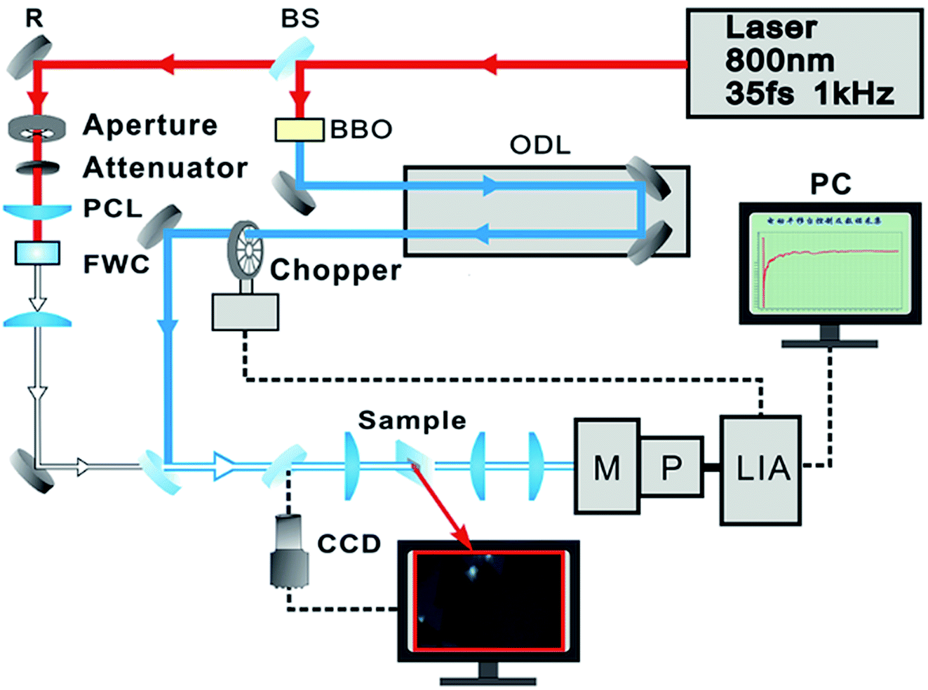 | ||
Fig. 2 The schematic diagram of a femtosecond transient absorption spectroscopy system: BS1 and BS2, 3![[thin space (1/6-em)]](https://www.rsc.org/images/entities/char_2009.gif) :7 and 1:1 beam splitter; BBO, 0.5 mm-thick β-BaB2O4 crystal; ODL, optical delay line; R, reflector; CL, convex lens; FWC, flow water cell; M, three grating monochromator; P, photomultiplier; LIA, lock-in amplifier. :7 and 1:1 beam splitter; BBO, 0.5 mm-thick β-BaB2O4 crystal; ODL, optical delay line; R, reflector; CL, convex lens; FWC, flow water cell; M, three grating monochromator; P, photomultiplier; LIA, lock-in amplifier. | ||
3. Results and discussion
Fig. 3(a) shows the optical micrograph of the as-synthesized MoS2 samples and it can be seen that the boundaries of different areas are very clear, and the two large homogeneous regions marked ‘1’ and ‘2’ were preliminarily identified to be layered MoS2. And the sizes of the samples at ‘1’ and ‘2’ are estimated to be about 130 μm2 and 450 μm2 with the assistance of a ruler scale. Moreover, to figure out the accurate layer number of the as-obtained MoS2 samples, Raman spectroscopy was further performed.29Fig. 3(b) shows the Raman spectra of the as-synthesized MoS2 samples located at the regions marked by ‘1’ and ‘2’ in Fig. 3(a). As can be seen, there are five Raman modes detected in the center of the Brillouin zone at region ‘1’, namely, shear mode (E22g) at 22.7 cm−1, breathing mode (B22g) at 40.27 cm−1, in-plane vibration mode (E12g) at 383.54 cm−1, out-of-plane vibration mode (A1g) at 405.46 cm−1,30 and the second-order longitudinal acoustic phonon mode (2LA(M)) at 452.21 cm−1.31 The positions of the peaks corresponding to these five Raman modes are in good agreement with the Raman eigenfrequency of bilayer MoS2 reported in a previous report;32 thus region “1” was identified to be bilayer MoS2.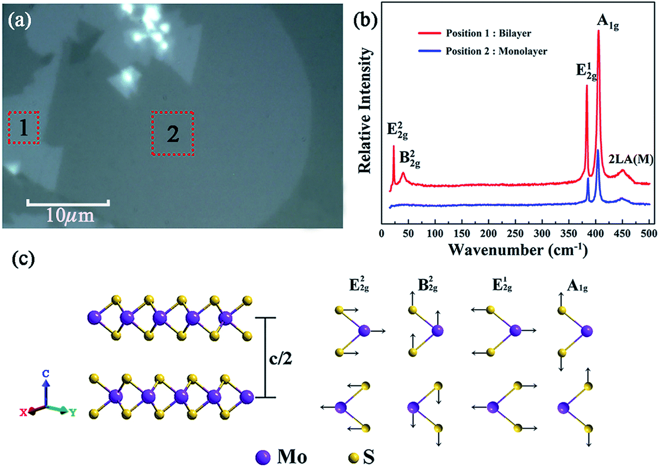 | ||
| Fig. 3 (a) Optical micrograph of layered MoS2 samples deposited on the quartz substrate; (b) Raman spectra of the as-synthesized MoS2 samples in the regions marked ‘1’ and ‘2’ in (a); (c) schematic diagrams of the lattice structure (left side) in out-of-plane directions of MoS2 and its corresponding characteristic Raman vibration modes (right side). | ||
Fig. 3(c) shows the schematic diagram of typical bilayer MoS2 and its corresponding characteristic vibration modes. It is clear that the B22g mode corresponds to a rigid-layer movement parallel to the c axis, and the E22g mode corresponds to a rigid-layer movement perpendicular to the c axis. Both of them exist only in two or more layers, so there should be no E22g and B22g modes when there is only a single layer of MoS2. Based on the above analysis, it can be seen from Fig. 3(b) that there are only three Raman modes (A1g, E12g and 2LA(M)) detected in the Raman spectra for region ‘2’, and the absence of E22g and B22g Raman signals implied that the region ‘2’ is monolayer MoS2.33
Fig. 4(a) presents the UV-vis absorption spectra of the monolayer and bilayer MoS2. As can be seen, there are two prominent absorption bands centered at 660 and 618 nm for both monolayer and bilayer MoS2. By contrast, the intensity of the absorption bands of bilayer MoS2 is much stronger than that of monolayer MoS2. The absorption band centered at 660 nm is well indexed to A excitons’ absorption, while the absorption band around 618 nm can be indexed to B excitons’ absorption.34 The absorption of A and B excitons is generally believed to be derived from the optical transition from the valence bands (Kv1 and Kv2) to the minimum of the conduction band (Kc) at the K point in the Brillouin zone, respectively, as schematically shown in Fig. 4(b). In addition, the energy difference between Kv1 and Kv2 bands stems from the splitting of the maximum valence band,35,36 which is believed to be caused by the combined effects of interlayer interactions and spin–orbit coupling for bilayer MoS2 and only the effect of spin–orbit coupling for monolayer MoS2.22,37
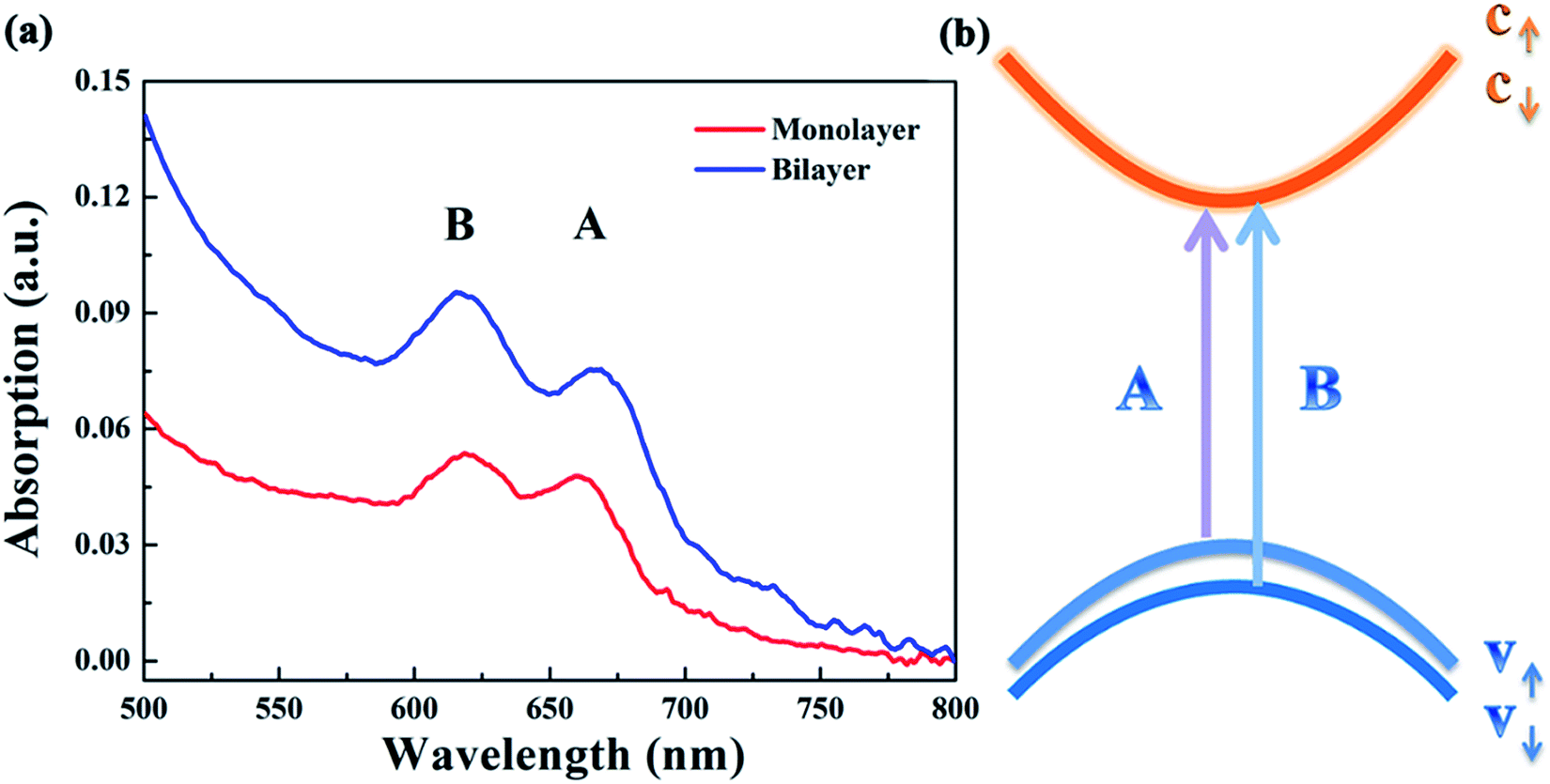 | ||
| Fig. 4 (a) The UV-vis absorption spectra of the as-grown monolayer and bilayer MoS2 after being returned to zero at 800 nm; (b) simplified band structure of MoS2 at the K point in the Brillouin zone. | ||
In spite of the above well-discussed different stable-state absorption properties of excitons caused by interlayer interactions, the influence of interlayer interactions on the relaxation dynamics of excitons in MoS2 still remains unknown and needs to be further addressed. Thus the influence of the interlayer interaction on exciton relaxation dynamics was further investigated with the assistance of our self-designed femtosecond transient absorption spectroscopy (fs-TAS) platform. Since the resonance absorption of A excitons for both monolayer and bilayer MoS2 was around 660 nm as shown in the UV-vis absorption spectra in Fig. 4(a), the probe laser wavelength was chosen to be 660 nm during the fs-TAS measurements. Besides, to guarantee the formation of photo-excited excitons at the A exciton level, the pump laser wavelength was set at 400 nm. And the pump intensity was selected to be 2 μJ cm−2 according to the linear relationship between the signal intensity and pump intensity (Fig. 5) to get strong and steady signals.
 | ||
| Fig. 5 Signal intensity of ΔT/T at zero time delay as a function of excitation intensity for (a) monolayer and (b) bilayer MoS2 with a pump wavelength of 400 nm and a probe wavelength of 660 nm. The circles denote the experimental data, while the solid lines denote the linear fitting data. | ||
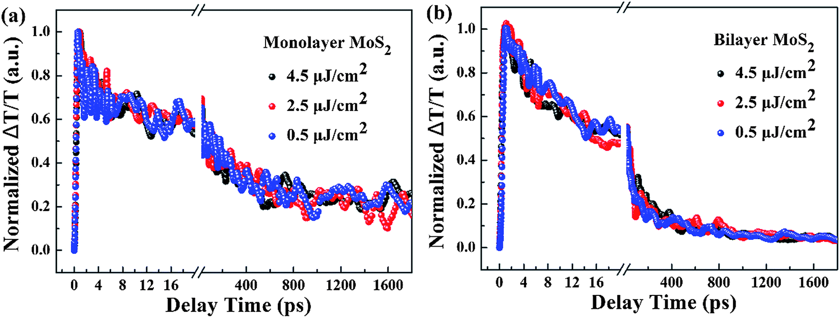
Fig. 6(a) displays the relaxation dynamics curves of A excitons for monolayer and bilayer MoS2. It is noteworthy that the relaxation time of bilayer MoS2 was much shorter than that of monolayer MoS2, which implies that the whole exciton relaxation became faster in the presence of interlayer interactions. Furthermore, the decay curves of monolayer and bilayer MoS2 were fitted separately and the fitting parameters for the decay curves are summarized in Table 1. As can be seen, both the relaxation dynamics signals of monolayer and bilayer MoS2 exhibit multi-exponential decays and can be fitted very well using a three exponential Gaussian response function of a1exp(−t/τ1) + a2exp(−t/τ2) + a3exp(−t/τ3), where τ1 < τ2 < τ3, which implies that multiple relaxation processes were involved. For monolayer MoS2, the decay was characterized by a fast decay time constant (τ1) of 3.3 ± 0.1 ps, an intermediate decay time constant (τ2) of 82.9 ± 5.6 ps and a slow decay time constant (τ3) of 1053.9 ± 26.6 ps, the proportion of the above three time constants was 35%, 20% and 45% in turn. Moreover, the relaxation lifetime of monolayer MoS2 is 489.5 ± 13.1 ps, which is close to the values in the literature,38 while for bilayer MoS2, the decay time constant was composed of a fast decay (τ1) of 3.7 ± 0.1 ps (31% weight), an intermediate decay (τ2) of 42.4 ± 0.8 ps (51% weight), and a slow decay (τ3) of 714.4 ± 25.1 ps (18% weight), and the relaxation lifetime is 150.7 ± 4.9 ps. The obviously changed proportion of the decay time constant and the significantly reduced relaxation lifetime for bilayer MoS2 imply that interlayer interactions have a significant effect on the relaxation characteristics of excitons.
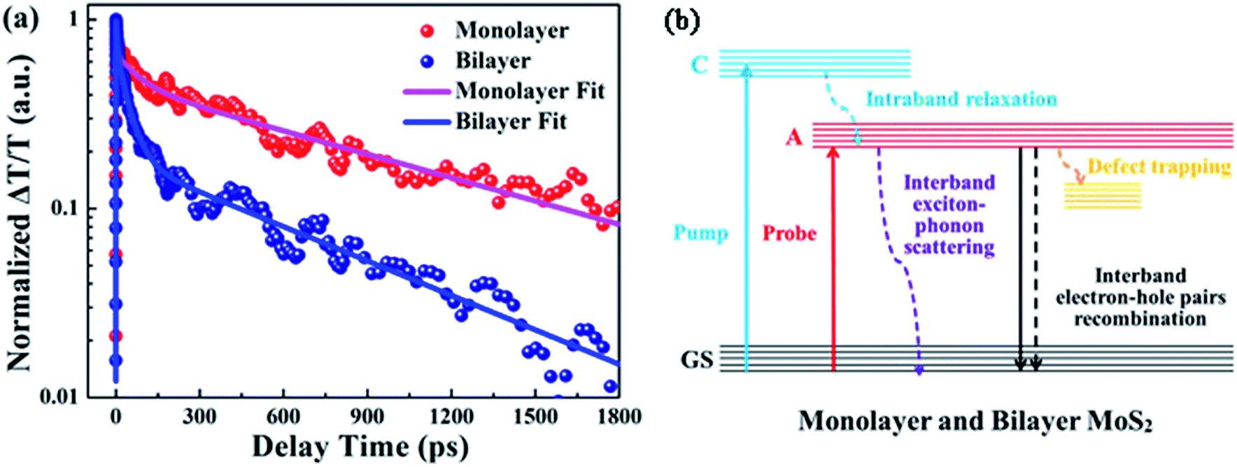 | ||
| Fig. 6 (a) Experimental (solid circles) and fitted (thick lines) data for normalized transient absorption relaxation dynamics curves of monolayer and bilayer MoS2. All the relaxation dynamics curves were normalized at time zero, being fitted with a three exponential function I(t) = a1exp(−t/τ1) + a2exp(−t/τ2) + a3exp(−t/τ3); (b) schematic summary of relaxation processes in monolayer and bilayer MoS2. | ||
exp(−t/τ1) + a2exp(−t/τ2) + a3exp(−t/τ3) with the fitting uncertainty. The percentage in the brackets represents the proportion of τ1, τ2 and τ3
| τ 1 (ps) | τ 2 (ps) | τ 3 (ps) | Lifetime (ps) | |
|---|---|---|---|---|
| Monolayer | 3.3 ± 0.1 (35%) | 82.9 ± 5.6 (20%) | 1053.9 ± 26.6 (45%) | 489.5 ± 13.1 |
| Bilayer | 3.7 ± 0.1 (31%) | 42.4 ± 0.8 (51%) | 717.4 ± 25.1 (18%) | 150.7 ± 4.9 |
To shed light on the underlying mechanism for the above dramatic reduction of the exciton relaxation time observed in bilayer MoS2, the transient absorption decay dynamics of monolayer and bilayer MoS2 were further characterized at different pump intensities, and the normalized dynamics curves are shown in Fig. 7. It can be seen that no significant dynamics dependences on the pump intensity were observed in either monolayer or bilayer MoS2, which indicates that the fast decay component was not the exciton–exciton annihilation process in this work. Since shallow and deep traps usually exist in MoS2 nanoclusters,39 and the fast decay time (τ1) obtained here is similar to the time scale of defect trapping;40 thus the fast decay component observed here was closely related to fast defect trapping. In addition, considering the characteristics of ultrathin MoS2, the exciton–phonon interaction is going to be very significant in monolayer and bilayer MoS2. Since the intermediate decay time constant (τ2) in our work was of the same order as the exciton–phonon scattering time reported in a recent study,40 the intermediate decay observed here might be attributed to the exciton–phonon scattering. The slowest decay process that lasted for hundreds of picoseconds (τ3) is generally believed to be derived from the recombination of electrons and holes. The schematic of the relaxation processes involved in monolayer and bilayer MoS2 is shown in Fig. 6(b).
 | ||
| Fig. 7 Normalized transient absorption decay dynamics curves of (a) monolayer and (b) bilayer MoS2 with a pump wavelength of 400 nm and a probe wavelength of 660 nm at different pump intensities. | ||
It is worth noting that unlike the similar values of τ1, the values of τ2 and τ3 for bilayer MoS2 were both significantly lower than those for monolayer MoS2. This dramatic enhancement of the exciton relaxation rate observed in bilayer MoS2 might be understood by the following aspects. Firstly, as can be seen from Fig. 3(b), the additional Raman vibration modes (B22g and E22g) and the stronger Raman vibration mode of A1g in bilayer MoS2 imply that the vibration of the atoms and lattice was enhanced due to the presence of interlayer interactions in comparison to monolayer MoS2.41 And the enhanced vibration of the lattice caused by the interlayer interaction will facilitate the exciton–phonon scattering in bilayer MoS2, resulting in a shorter intermediate decay time τ2.
Secondly, since monolayer MoS2 is a direct band-gap semiconductor, most of the electrons and holes are located on the conduction band minimum (CBM) and valence band maximum (VBM) at the K point, respectively; thus the radiative recombination of electrons and holes happens very easily, which can be verified by the extremely strong photoluminescence (PL) intensity of monolayer MoS2 as shown in Fig. 8. Therefore, the main recombination process of electrons and holes in monolayer MoS2 is radiative recombination. However, bilayer MoS2 is an indirect band-gap semiconductor, the photon energy (3.1 eV) employed here will pump the initial carriers to a higher energy level, and the fast cooling of the carriers would let the electrons and holes locate on the CBM at the K point and the VBM at the Γ point,2 respectively. Thus, the radiative recombination of electrons and holes in bilayer MoS2 requires the assistance of phonons,42 which will significantly suppress the radiative relaxation process in bilayer MoS2. Moreover, many previous reports have proved that the interlayer interaction can redistribute the charges , which gives rise to a local electric field at the interfacial region in bilayer MoS2. After being excited by the pump beam, the electrons will accumulate at the interfacial surfaces, while the holes will thus be pushed away from the interface due to the local electric field, which will lead to spatial separation of electrons and holes. And the reduction of the overlap between electron and hole wavefunctions will make the relaxation of electrons and holes through radiative recombination difficult, resulting in the decrease of fluorescence quantum yield.27 This can also be seen in the PL spectra shown in Fig. 8. It can be seen from Fig. 8 that the PL intensity of A excitons reduced dramatically in bilayer MoS2, which suggests that the radiative recombination becomes negligible in bilayer MoS2 compared to monolayer MoS2. Therefore, the prominent recombination process of electrons and holes in bilayer MoS2 is non-radiative recombination. Furthermore, it is well known that the decay time of non-radiative recombination is usually shorter than that of radiative recombination.43,44 Therefore the decay time τ3 of bilayer MoS2 is much shorter than that of monolayer MoS2. Given the above, it therefore can be concluded that the dramatic enhancement of the whole relaxation rate of A excitons for bilayer MoS2 can be explained by the combined effects of the enhanced exciton–phonon scattering and reduced radiative relaxation induced by interlayer interactions.
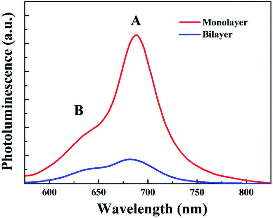 | ||
| Fig. 8 Photoluminescence (PL) spectra of monolayer and bilayer MoS2. | ||
4. Conclusions
In summary, we performed a detailed investigation into the underlying influence of interlayer interactions on the relaxation dynamics of excitons in ultrathin MoS2 by analyzing the discrepancy in relaxation dynamics and photoluminescence properties only between bilayer MoS2 and monolayer MoS2. On the basis of thoughtful analysis about the obtained experimental data, both monolayer and bilayer MoS2 samples exhibit multiple relaxation processes involving the defect trapping, the exciton–phonon scattering, and the recombination process of electrons and holes. Moreover, the characterization results manifest that the relaxation rate of A excitons was significantly accelerated in bilayer MoS2 compared to monolayer MoS2, which is due to the combined effects of the enhanced exciton–phonon scattering and reduced radiative relaxation induced by interlayer interactions.Conflicts of interest
There are no conflicts to declare.Acknowledgements
We are grateful to Prof. Yisong Zheng and Prof. Jianzhong Zhang for many fruitful discussions. We also thank Prof. Kai Wang and researcher Guohui Lu for their help during the experimental research. This work was supported by the financial support from the National Natural Science Foundation of China (no. 11274137, 11574112, 11474127, 51304080).References
- K. F. Mak, C. Lee, J. Hone, J. Shan and T. F. Heinz, Phys. Rev. Lett., 2010, 105, 136805 CrossRef PubMed.
- X. M. Dou, K. Ding, D. S. Jiang and B. Q. Sun, ACS Nano, 2014, 8, 7458–7464 CrossRef CAS PubMed.
- A. R. Klots, A. K. M. Newaz, B. Wang, D. Prasai, H. Krzyzanowska, J. H. Lin, D. Caudel, N. J. Ghimire, J. Yan, B. L. Ivanov, K. A. Velizhanin, A. Burger, D. G. Mandrus, N. H. Tolk, S. T. Pantelides and K. I. Bolotin, Sci. Rep., 2014, 4, 6608 CrossRef CAS PubMed.
- N. Saigal, V. Sugunakar and S. Ghosh, Appl. Phys. Lett., 2016, 108, 132105 CrossRef.
- T. Cao, G. Wang, W. P. Han, H. Q. Ye, C. R. Zhu, J. R. Shi, Q. Niu, P. H. Tan, E. Wang, B. L. Liu and J. Feng, Nat. Commun., 2012, 3, 887 CrossRef PubMed.
- K. F. Mak, K. L. He, J. Shan and T. F. Heinz, Nat. Nanotechnol., 2012, 7, 494–498 CrossRef CAS PubMed.
- G. L. Frey, K. J. Reynolds, R. H. Friend, H. Cohen and Y. Feldman, J. Am. Chem. Soc., 2003, 125, 5998–6007 CrossRef CAS PubMed.
- G. J. Choi, Q. V. Le, K. S. Choi, K. C. Kwon, H. W. Jang, J. S. Gwag and S. Y. Kim, Adv. Mater., 2017, 29, 1702598 CrossRef PubMed.
- K. P. Guo, C. F. Si, C. Han, S. H. Pan, G. Chen, Y. Q. Zheng, W. Q. Zhu, J. H. Zhang, C. Sun and B. Wei, Nanoscale, 2017, 9, 14602–14611 RSC.
- Y. X. Deng, Z. Luo, N. J. Conrad, H. Liu, Y. J. Gong, S. Najmaei, P. M. Ajayan, J. Lou, X. F. Xu and P. D. Ye, ACS Nano, 2014, 8, 8292–8299 CrossRef CAS PubMed.
- Y. Niu, R. Frisenda, S. A. Svatek, G. Orfila, F. Gallego, P. Gant, N. Agrait, C. Leon, A. Rivera-Calzada, D. P. De Lara, J. Santamaria and A. Castellanos-Gomez, 2D Mater., 2017, 4, 034002 CrossRef.
- Z. Li, J. H. Chen, R. Dhall and S. B. Cronin, 2D Mater., 2017, 4, 015004 CrossRef.
- X. Gu, W. Cui, H. Li, Z. W. Wu, Z. Y. Zeng, S. T. Lee, H. Zhang and B. Q. Sun, Adv. Energy Mater., 2013, 3, 1262–1268 CrossRef CAS.
- M. L. Tsai, S. H. Su, J. K. Chang, D. S. Tsai, C. H. Chen, C. I. Wu, L. J. Li, L. J. Chen and J. H. He, ACS Nano, 2014, 8, 8317–8322 CrossRef CAS PubMed.
- A. Capasso, F. Matteocci, L. Najafi, M. Prato, J. Buha, L. Cina, V. Pellegrini, A. Di Carlo and F. Bonaccorso, Adv. Energy Mater., 2016, 6, 1600920 CrossRef.
- G. H. Lee, Y. J. Yu, X. Cui, N. Petrone, C. H. Lee, M. S. Choi, D. Y. Lee, C. Lee, W. J. Yoo, K. Watanabe, T. Taniguchi, C. Nuckolls, P. Kim and J. Hone, ACS Nano, 2013, 7, 7931–7936 CrossRef CAS PubMed.
- B. Radisavljevic, A. Radenovic, J. Brivio, V. Giacometti and A. Kis, Nat. Nanotechnol., 2011, 6, 147–150 CrossRef CAS PubMed.
- H. Ji, H. Yi, J. Seok, H. Kim, Y. H. Lee and S. C. Lim, Nanoscale, 2018, 10, 10856–10862 RSC.
- S. Bertolazzi, J. Brivio and A. Kis, ACS Nano, 2011, 5, 9703–9709 CrossRef CAS PubMed.
- W. S. Yun, S. W. Han, S. C. Hong, I. G. Kim and J. D. Lee, Phys. Rev. B, 2012, 85, 033305 CrossRef.
- A. Splendiani, L. Sun, Y. B. Zhang, T. S. Li, J. Kim, C. Y. Chim, G. Galli and F. Wang, Nano Lett., 2010, 10, 1271–1275 CrossRef CAS PubMed.
- T. Cheiwchanchamnangij and W. R. L. Lambrecht, Phys. Rev. B, 2012, 85, 205302 CrossRef.
- Y. L. Yan, F. F. Li, Y. B. Gong, M. G. Yao, X. L. Huang, X. P. Fu, B. Han, Q. Zhou and T. Cui, J. Phys. Chem. C, 2016, 120, 24992–24998 CrossRef CAS.
- X. M. Dou, K. Ding, D. S. Jiang, X. F. Fan and B. Q. Sun, ACS Nano, 2016, 10, 1619–1624 CrossRef CAS PubMed.
- S. W. Han, H. Kwon, S. K. Kim, S. Ryu, W. S. Yun, D. H. Kim, J. H. Hwang, J. S. Kang, J. Baik, H. J. Shin and S. C. Hong, Phys. Rev. B, 2011, 84, 045409 CrossRef.
- A. F. Rigos, H. M. Hill, Y. L. Li, A. Chernikov and T. F. Heinz, Nano Lett., 2015, 15, 5033–5038 CrossRef PubMed.
- J. G. Kim, W. S. Yun, S. Jo, J. Lee and C. H. Cho, Sci. Rep., 2016, 6, 29813 CrossRef CAS PubMed.
- Y. H. Lee, X. Q. Zhang, W. J. Zhang, M. T. Chang, C. T. Lin, K. D. Chang, Y. C. Yu, J. T. W. Wang, C. S. Chang, L. J. Li and T. W. Lin, Adv. Mater., 2012, 24, 2320–2325 CrossRef CAS PubMed.
- T. Sekine, K. Uchinokura, T. Nakashizu, E. Matsuura and R. Yoshizaki, J. Phys. Soc. Jpn., 1984, 53, 811–818 CrossRef CAS.
- T. Wieting and J. Verble, Phys. Rev. B, 1971, 3, 4286–4292 CrossRef.
- H. Li, Q. Zhang, C. C. R. Yap, B. K. Tay, T. H. T. Edwin, A. Olivier and D. Baillargeat, Adv. Funct. Mater., 2012, 22, 1385–1390 CrossRef CAS.
- Y. Zhao, X. Luo, H. Li, J. Zhang, P. T. Araujo, C. K. Gan, J. Wu, H. Zhang, S. Y. Quek and M. S. Dresselhaus, Nano Lett., 2013, 13, 1007–1015 CrossRef CAS PubMed.
- H. Zeng, B. Zhu, K. Liu, J. Fan, X. Cui and Q. Zhang, Phys. Rev. B, 2012, 86, 241301 CrossRef.
- R. Coehoorn, C. Haas and R. De Groot, Phys. Rev. B, 1987, 35, 6203–6206 CrossRef CAS.
- B. Evans and P. Young, Proc. Phys. Soc., 1967, 91, 475–482 CrossRef CAS.
- J. Wilson and A. Yoffe, Adv. Phys., 1969, 18, 193–335 CrossRef CAS.
- R. F. Frindt, Phys. Rev., 1965, 140, A536–A539 CrossRef.
- L. Yang, D. Zhong, J. Y. Zhang, Z. P. Yan, S. F. Ge, P. W. Du, J. Jiang, D. Sun, X. J. Wu, Z. Y. Fan, S. A. Dayeh and B. Xiang, ACS Nano, 2014, 8, 6979–6985 CrossRef CAS PubMed.
- R. Doolen, R. Laitinen, F. Parsapour and D. F. Kelley, J. Phys. Chem. B, 1998, 102, 3906–3911 CrossRef CAS.
- T. Korn, S. Heydrich, M. Hirmer, J. Schmutzler and C. Schuller, Appl. Phys. Lett., 2011, 99, 102109 CrossRef.
- C. Lee, H. Yan, L. E. Brus, T. F. Heinz, J. Hone and S. Ryu, ACS Nano, 2010, 4, 2695–2700 CrossRef CAS PubMed.
- H. Dery and Y. Song, Phys. Rev. B, 2015, 92, 125431 CrossRef.
- L. Y. Pan, Y. L. Zhang, H. Y. Wang, H. Liu, J. S. Luo, H. Xia, L. Zhao, Q. D. Chen, S. P. Xu, B. R. Gao, L. M. Fu and H. B. Sun, Nanoscale, 2011, 3, 2882–2888 RSC.
- M. Palummo, M. Bernardi and J. C. Grossman, Nano Lett., 2015, 15, 2794–2800 CrossRef CAS PubMed.
| This journal is © The Royal Society of Chemistry 2019 |