
 Open Access Article
 This Open Access Article is licensed under a
 Creative Commons Attribution 3.0 Unported Licence
Tunable transport and optoelectronic properties of monolayer black phosphorus by grafting PdCl2 quantum dots†
Cuicui Sun ,
Yuxiu Wang,
Yingjie Jiang,
Zhao-Di Yang,
Guiling Zhang* and
Yangyang Hu*
,
Yuxiu Wang,
Yingjie Jiang,
Zhao-Di Yang,
Guiling Zhang* and
Yangyang Hu*
School of Materials Science and Engineering, College of Chemical and Environmental Engineering, Harbin University of Science and Technology, Harbin 150080, China. E-mail: guiling-002@163.com
First published on 15th October 2018
Abstract
The electronic, transport, and optoelectronic properties of monolayer black phosphorus (MLBP) are much influenced by grafting PdCl2 groups, demonstrated here by using density functional theory (DFT) and non-equilibrium Green's function (NEGF) as well as the Keldysh Nonequilibrium Green's Functions (KNEGF) methods. We find that the PdCl2 groups prefer to locate over the furrow site of MLBP and form a planar quadridentate structure of 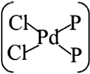 . The PdCl2 groups serve as quantum dots by introducing discrete flat levels between the MLBP valence band and the Fermi level (Ef). The conductivity is much lowered after attaching PdCl2 quantum dots, due to the fact that the scattering effect of PdCl2 plays a major role in the process of electron transporting. A threshold voltage is found for the functionalized system with a large density of PdCl2 quantum dots, a valuable clue for exploring current switches. However, no evident threshold voltage is found for the pure MLBP. Electrons permeate easier through the armchair direction compared with the zigzag either in the pure MLBP or in the functionalized composites. More importantly, grafting PdCl2 quantum dots is very beneficial for enhancing photoresponse. The values of photoresponse for the modified species are about 20 times higher than the free MLBP. A significant photoresponse anisotropy is observed for both MLBP and nPdCl2-BP (n = 1, 2, and 4), contrary to the conductivity, the zigzag direction shows much stronger photoresponse than the armchair. All of the aforementioned unique properties make these new two-dimensional (2D) MLBP based materials especially attractive for both electronic and optoelectronic devices.
1. Introduction
Inspired by the great achievements of graphene, two-dimensional (2D) nanomaterials have received great attention in the fields of micro-/nano-electronics and optoelectronics due to their distinct confinement effect of electrons in two dimensions,1 strong in-plane covalent interactions,2 large lateral size,3 high exposure of surface,4 and so forth. After graphene with zero band gap5 and molybdenum disulphide with relatively low carrier mobility,6 monolayer black phosphorus (MLBP) has emerged as an important member of 2D materials family7 in recent years. In this layer, each P atom bonds to three neighboring P atoms through sp3 hybridized orbitals forming warped hexagons in a nonplanar fashion. To date, many production methods for MLBP have been developed, including liquid exfoliation,8–12 Ar+ plasma thinning process,13 photochemical etching,14 and mechanical exfoliation,15,16 etc. Importantly, it has enormous potential to be used in high-performance electronic and optoelectronic devices because of its direct tunable band gap ranging from 0.3 to 2.0 eV,17,18 high carrier mobility of ∼1000 cm2 V−1 s−1 at room temperature,7,17,19 and anisotropic optical characteristics20,21 that could complement or exceed graphene and molybdenum disulphide in the next generation of novel devices.In the electronic arrangement, the P atom with a valence shell configuration 3s23p3 has five valence electrons available for bonding, and the existence of the lone pair makes MLBP reactive to air. Functionalization is proved to be an controllable and effective method to not only improve the stability but also to enrich the property22,23 of 2D materials. Tunability of electronic properties of 2D materials is crucial for their practical applications in electronics and optoelectronics. Up to now, many functionalized 2D black phosphorus (BP) have been reported, such as metal/BP contact systems,24–27 alkali metal/nonmetal atom doped BP,28–31 carbon nanotube/BP composites,32 as well as hBN/BP33–35 and MoS2/BP36,37 heterojunctions. Out of the above mentioned series, the most recent addition to the family are the functionalization of BP38,39 by adsorbing transition metal atoms on surface.40–44 It has been found that palladium (Pd) adatom adsorption on MLBP presents excellent electronic and optoelectronic behaviors.41–43 Up to now, research on functionalization of MLBP is predominantly focused on its physical modification; far less information is available regarding chemical modification, which is determined to be efficient in manipulating electronic and optoelectronic properties.45
In general, the Pd atom is a typical transition metal for coordinating P and Cl ligands.46–48 These complexes have shown wide spread applications in electronics, photoelectrochemistry, and electrochemistry.49–51 Usually, Pd has a 4d10 configuration and preferentially provides a dsp2 hybrid environment to coordinate with four ligands, i.e., forms a planar quadridentate complex. The exposed P atoms of MLBP are perfect ligands by providing lone pair electrons to coordinate with the Pd atom of PdCl2 to form a planar quadridentate structure of  . Of particular interest in this paper is investigation of covalent functionalization of MLBP with PdCl2 groups including the effects of PdCl2 on electronic, transport, and optoelectronic properties.
2. Models and computational methods
For the periodic systems, we constructed the supercell as 2 × 4 (x × y) containing 32 P atoms (Fig. 1). We selected n PdCl2 groups (referred as nPdCl2, where n = 1, 2, and 4) to graft MLBP per supercell to study the effects of grafting density n. Hereafter, the functioned structures are denoted as nPdCl2-BP (n = 1, 2, and 4) for simplification. For the geometrical optimization, the PdCl2 was put at each adsorption site with all the atomic coordinates in the system being relaxed. The maximum force and maximum stress were set to the same value of 0.02 eV Å−1.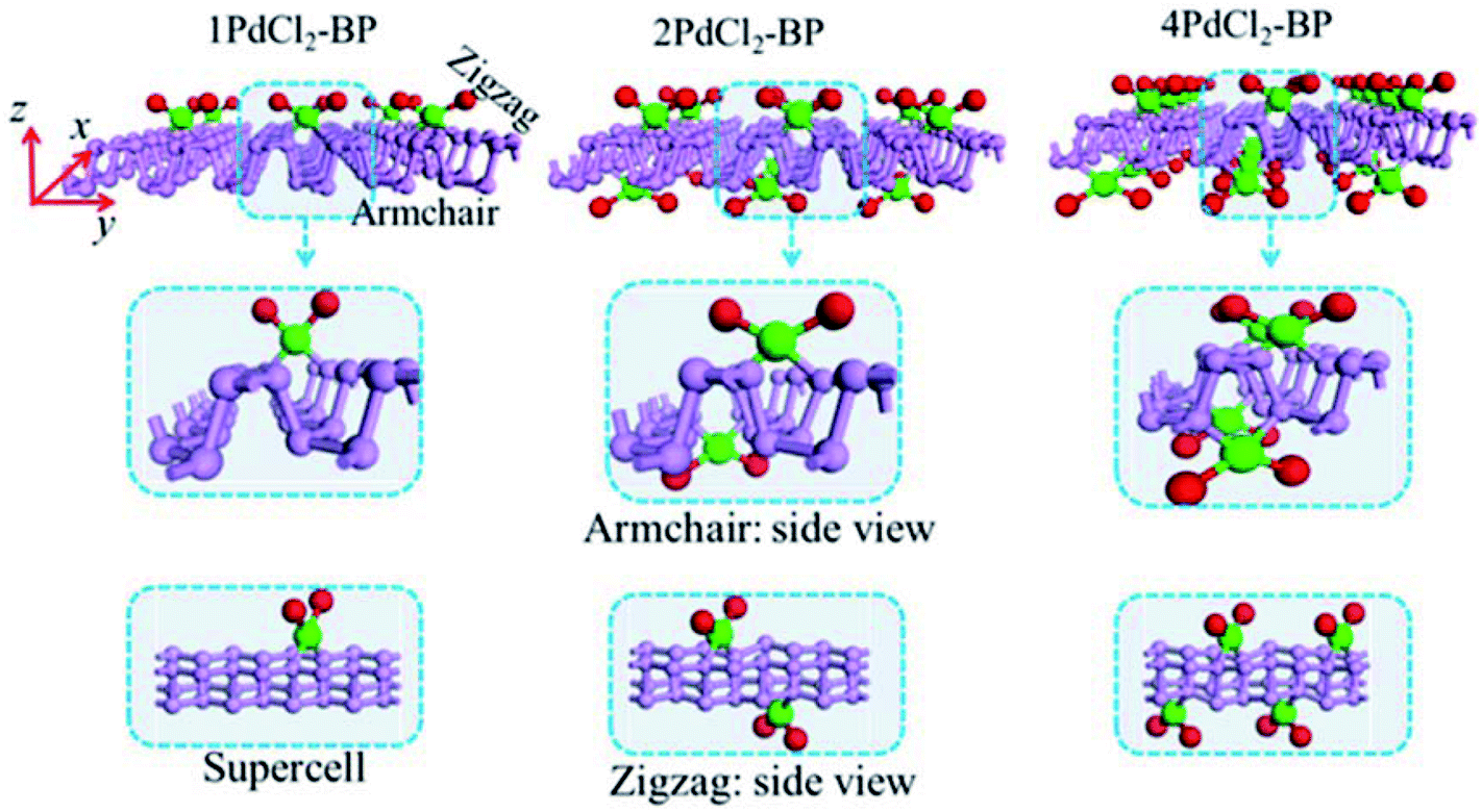 | ||
| Fig. 1 Optimized structures of three most stable systems of 1PdCl2-BP, 2PdCl2-BP, and 4PdCl2-BP. | ||
It has been reported that the MLBP displays anisotropic properties due to its anisotropic structure,52,53 which triggered us to calculate transport and optoelectronic properties for two mutually perpendicular directions, i.e., the armchair and zigzag directions (Fig. 2(a and c) vs. 2(b and d)). So we curved a nearly square plane (∼26.04 Å × 26.50 Å) of MLBP and nPdCl2-BP (n = 1, 2, and 4) as the scatter region to be sandwiched between two Au (100)-(9 × 3) electrodes to build two-probe devices. Such scatter region was formed by repeating each optimized supercell 3 times at the armchair direction and 2 times at the zigzag direction. When the scatter region used the zigzag edge to connect with the Au electrodes, the armchair direction properties were calculated (denoted as a-MLBP and a-nPdCl2-BP (n = 1, 2, and 4)). Another was just the reverse (nominated as z-MLBP and z-nPdCl2-BP (n = 1, 2, and 4)). As a benchmark test, the Ef positions of the two-probe systems with two or four buffer layers of Au were calculated at 0.0 V. We found that the Ef were almost locate at the same positions for the two cases (−3.533772 and −3.533858 eV for the two and four buffer layers, respectively). So we used two buffer layers of Au to perform further calculations. The nearest P–Au distance is 2.37 Å, corresponding to their covalent bonding.54 Transport current was computed by changing the applied bias voltage in the step of 0.2 V in the range of −1.0 to 1.0 V.
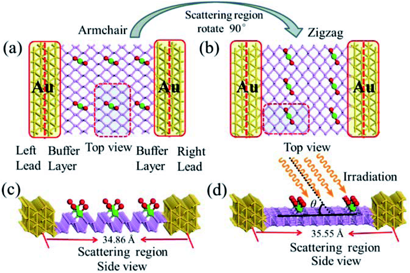 | ||
| Fig. 2 Exemplified two-probe devices by 1PdCl2-BP. (a) Top view of a-1PdCl2-BP; (b) top view of z-1PdCl2-BP; (c) side view of a-1PdCl2-BP; (d) side view of z-1PdCl2-BP. Irradiation on the scatter regions of two-probe devices are schematically shown in (d). | ||
Electronic and transport property computations were performed by using the software package Atomistix ToolKit (ATK)55–58 based on a basis of the combination of density function theory (DFT) and non-equilibrium Green's function (NEGF) methods. The on-site correlation effect among 4d electrons of the Pd atom was accounted for by using the GGA+U scheme58 where the parameter U–J was set to be 6.0 based on the literature (6.0),59 which was also close to that (5.77) in the ATK_U database. The Perdew–Burke–Ernzerhof (PBE) exchange–correlation functional was employed. A single-ζ basis with polarization (SZP) was used for all atoms. A (7 × 5 × 1) K-point in the Brillouin zone (x, y, and z directions, respectively) was adopted, and 150 Ry cutoff energy was applied to describe the periodic wave function.
To gain an insight into the optoelectronic properties of MLBP and nPdCl2-BP (n = 1, 2, and 4), we irradiated the scatter regions of above mentioned two-probe systems with linearly polarized light (exemplified as Fig. 2(d)). The polarized angle θ was assigned between the scatter region plane and the irradiation direction. The photo energy was set from 0.0 to 1.0 eV with an interval of 0.1 eV. We calculated the photocurrent varying with θ from 0° to 180° at the 0.0 V bias voltage.
The optoelectronic properties of a-MLBP, z-MLBP, a-nPdCl2-BP, and z-nPdCl2-BP (n = 1, 2, and 4) were evaluated using the Nanodcal60 package which carried out DFT within the Keldysh Nonequilibrium Green's Functions (KNEGF).60,61 Standard norm-conserving nonlocal pseudopotentials were adopted to define the atomic cores, and SZP linear combination of atomic orbital basis set was used to expand physical quantities. The exchange–correlation potential was treated at the GGA+U with PBE.
3. Results and discussions
3.1 Stability and geometry
The MLBP is not residing in a flatland, instead, it forms a puckered hexagonal structure. The optimized supercell vectors of MLBP and nPdCl2-BP (n = 1, 2, and 4) were supplied in Table S1 in the ESI.† On the surface of this supercell one, two, or four PdCl2, corresponding to n = 1, 2, or 4, respectively, are considered to coordinate with the P atom for investigating the effect of grafting density. Taking into account all the circumstances, 20 configurations are computed for nPdCl2-BP (n = 1, 2, and 4), i.e., 2 for 1PdCl2-BP, 10 for 2PdCl2-BP, and 8 for 4PdCl2-BP. Table S2 in the ESI† summarizes the optimized total energies of supercells of these 20 configurations. We find that the PdCl2 groups prefer to locate over the furrow site rather than upon the ridge position of the MLBP as the former has lower total energy than the latter. A planar structure of is formed in these nPdCl2-BP complexes, a typical quadridentate structure for Pd. As for 2PdCl2-BP and 4PdCl2-BP, the PdCl2 components tend to evenly and staggerly distributed on both sides of MLBP. Finally, we chose three most stable configurations for n = 1, 2, and 4, respectively, as given in Fig. 1, to further investigate the electronic, transport, and optoelectronic properties.
For the three most stable structures of 1PdCl2-BP, 2PdCl2-BP, and 4PdCl2-BP, we have calculated the binding energies, Eb, by using Eb = EnPdCl2-BP − EMLBP − nEPdCl2, where EnPdCl2-BP, EMLBP, and EPdCl2 denote the total energies of the functioned systems, pristine MLBP, and PdCl2 in the unit cell, respectively. For the PdCl2 calculation, the unit cell was set to be 30 × 30 × 30 Å, so that PdCl2 can be viewed as an isolated system. The calculated binding energies are all negative with increasing exoenergic values of −1.95, −3.83, and −7.35 eV from n = 1, 2 to 4 (Table 1), demonstrating that grafting PdCl2 groups to the MLBP surface is energetically favorable.
| Species | Eb (eV) | rinP–P (Å) | routP–P (Å) | rPd–P (Å) | rPd–Cl (Å) | DPd–Pd (Å) | DCl–Cl (Å) |
|---|---|---|---|---|---|---|---|
| MLBP | — | 2.224 | 2.244 | — | — | — | — |
| 1PdCl2-BP | −1.95 | 2.264 | 2.307 | 2.363 | 2.447 | — | — |
| 2PdCl2-BP | −3.83 | 2.268 | 2.345 | 2.364 | 2.442 | 6.359 | 7.667 |
| 4PdCl2-BP | −7.35 | 2.271 | 2.365 | 2.373 | 2.438 | 6.627 | 6.205 |
After optimizing, the P–P, Pd–P, Pd–Cl, and Pd–Pd bond lengths as well as the Cl–Cl distances for MLBP and nPdCl2-BP (n = 1, 2, and 4) are collected in Table 1. MLBP consists of double puckered planes; each atom is bound to two in-plane atoms with a bond length of rinP–P = 2.224 Å and to one out-of-plane atom with a bond length of routP–P = 2.244 Å, fully in agreement with experimental observation.62 For nPdCl2-BP (n = 1, 2, and 4), the Pd–P bond lengths are rPd–P = 2.363–2.374 Å, in line with genral Pd–P chemical bond lengths calculated by M. A. Carvajal et al.63 (2.221–2.476 Å) and experimental data reported by V. I. Bakhmutov et al. (2.290–2.520 Å).47 This shows that the covalent bonds are formed between grafted PdCl2 groups and the P atoms. These P atoms (bonded to Pd) are pushed slightly inward (toward another plane), consequently, the rinP–P and routP–P are elongated to 2.264–2.271 Å and 2.307–2.365 Å, respectively. The Pd–Cl bond lengths in nPdCl2-BP (n = 1, 2, and 4) are about rPd–Cl = 2.429–2.457 Å, in accordance with literature reported values of 2.333–2.575 Å.63 For nPdCl2-BP (n = 1, 2, and 4), the nearest Cl–Cl distances (DCl–Cl) or Pd–Pd distances (DPd–Pd) between two adjacent PdCl2 are all longer than 6.0 Å, implying negligible PdCl2–PdCl2 interactions in these considered systems.
3.2 Band structure
The band structure and projected density of states (PDOS) as well as the Kohn–Sham orbitals near the Fermi level (Ef) of MLBP and nPdCl2-BP (n = 1, 2, and 4) were calculated as shown in Fig. 3 and 4. Clearly, the MLBP shows a semiconductive feature with a direct band gap (Eg) of 0.85 eV, in agreement with the previous report value about 0.90 eV.64–66 Decoration of PdCl2 groups on MLBP surface can tune the transport property by altering the electronic structure. They may carry properties exhibited by each component as well as new properties generated as a result of their combination.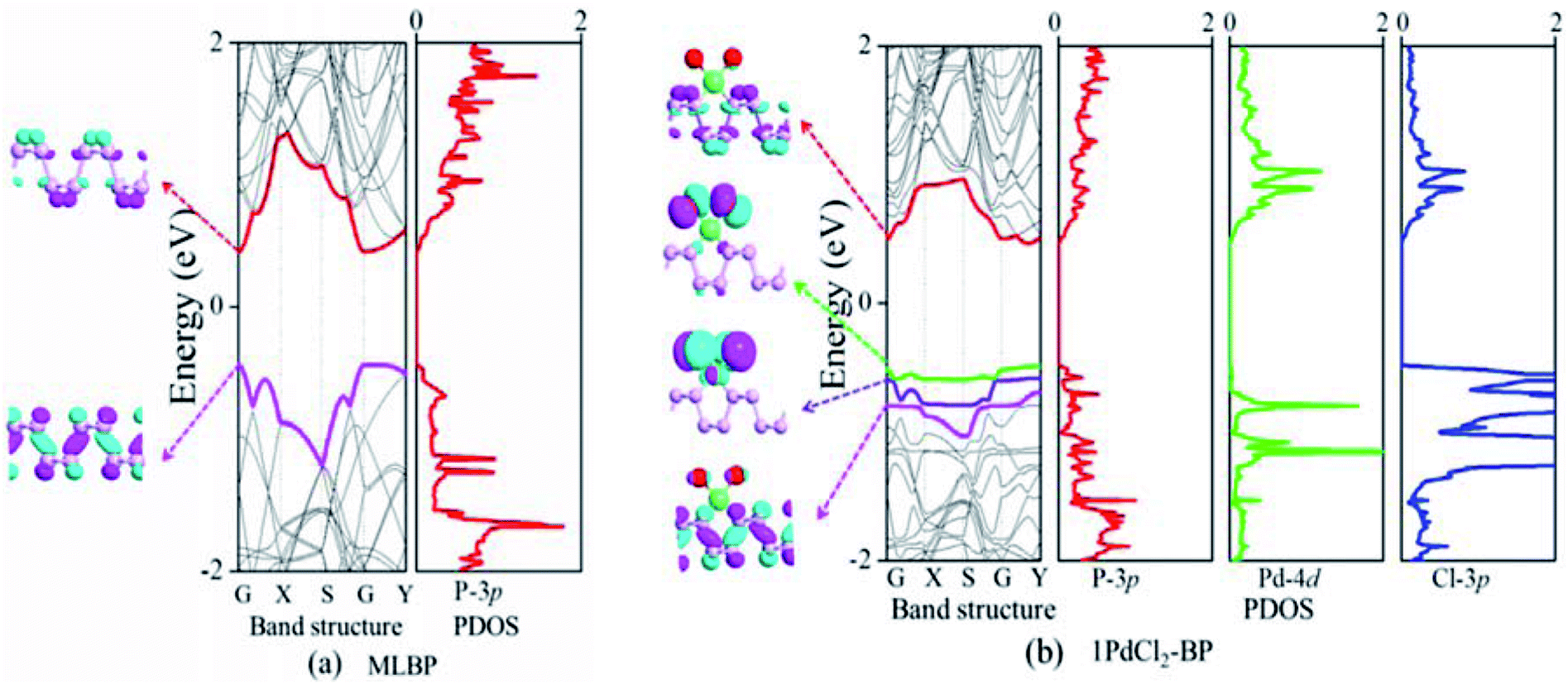 | ||
| Fig. 3 For (a) MLBP and (b) 1PdCl2-BP, computed band structures and PDOS as well as the Kohn–Sham orbital corresponding to the energy levels (highlighted in color lines) near Ef at the Γ point. The iso-surface value is 0.028 (e Å−3). | ||
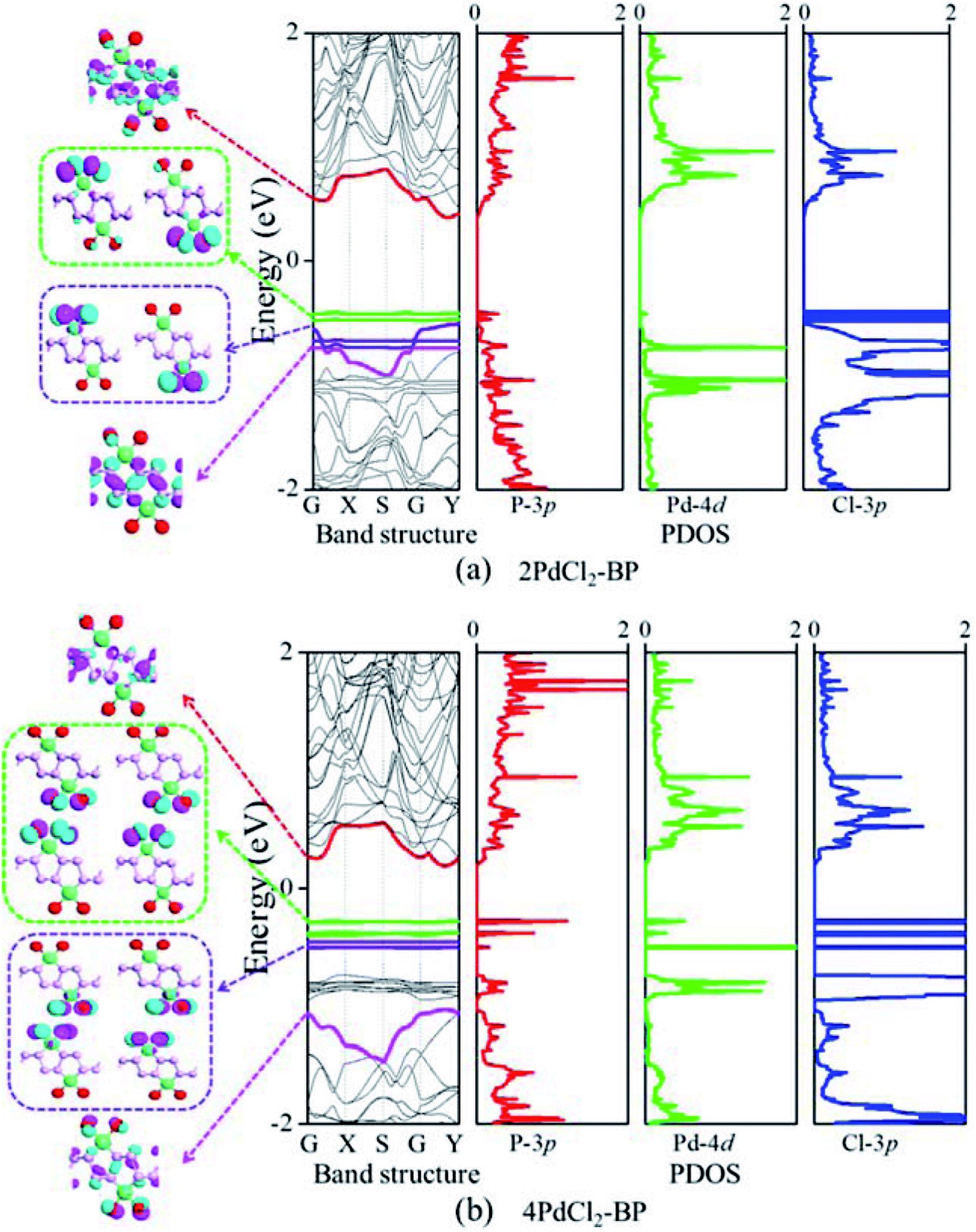 | ||
| Fig. 4 For (a) 2PdCl2-BP and (b) 4PdCl2-BP, computed band structures and PDOS as well as the Kohn–Sham orbital corresponding to the energy levels (highlighted in color lines) near Ef at the Γ point. The iso-surface value is 0.028 (e Å−3). | ||
We can evidently find that nPdCl2-BP introduces flat PdCl2 bands just above the MLBP valence band and below the Ef, indicating that the PdCl2 groups contribute localized states in the MLBP band gap region. The Kohn–Sham orbitals also clearly demonstrate the localized character of PdCl2 groups. The dispersion of some PdCl2 band structures around the Γ may be attributed to the large interaction between the Pd and Cl atoms. Correspondingly, PdCl2 groups give sharp PDOS peaks as localized valence states. In this sense, the anchored PdCl2 groups behave as quantum dots. These quantum dots mainly originate from the Cl-3p state as can be seen from its large PDOS. In general, quantum dots can form ionic like or covalent like interaction.67 In the former case, the electrons are localized on the individual dots which exhibit a weak tunnel coupling. For the latter, quantum dot electron states are quantum-mechanically coupled and show strong tunnel coupling. Clearly, nPdCl2-BP (n = 1, 2, and 4) systems bear spatially separated PdCl2 quantum dots with localized and discrete energy levels owing to the large separations between PdCl2 quantum dots, electron tunneling through direct coupling of PdCl2 is minor.
For a general planar quadridentate complex, the ligand field splitting of the Pd 4d electrons results in molecular orbitals being formed of principally a character of eg (dyz,zx), a1g (dz2), b2g (dxy), and b1g (dx2–y2). The former eg (dyz,zx) and a1g (dz2) are electron occupied leaving b2g (dxy) and b1g (dx2–y2) to be unoccupied. We can see from the PDOS, clearly, the eg (dyz,zx) molecular orbitals locate just below the Ef. Usually, the Pd quadridentate compounds belong to inner-orbital complexes with a zero magnetic moment. In nPdCl2-BP, the Cl2P2 ligands generate an uneven ligand field leading to a so-called Jahn–Teller effect. Pd forms a dsp2 hybrid environment to interact with the 3p orbitals of the P and Cl atoms. As a result, the degenerate orbitals of eg (dyz,zx) are again split. Therefore, discrete bands appear in the MLBP band gap region of nPdCl2-BP (n = 1, 2, and 4).
To further investigate the interactions between MLBP and PdCl2, we calculated the electron difference densities for nPdCl2-BP (n = 1, 2, and 4) systems and the results are plotted in Fig. 5. The electron difference density refers to the difference between the self-consistent valence charge density and the superposition of atomic valence density, which indicates the coupling between the atoms in a certain system. The green area means no electron transfer, red part represents obtaining electrons, while blue region indicates losing electrons. Charge transfers from the MLBP substrate to the PdCl2 quantum dots can be observed from Fig. 5, suggesting a strong coupling between MLBP and PdCl2, which is an important factor in tuning the electronic and optoelectronic properties.
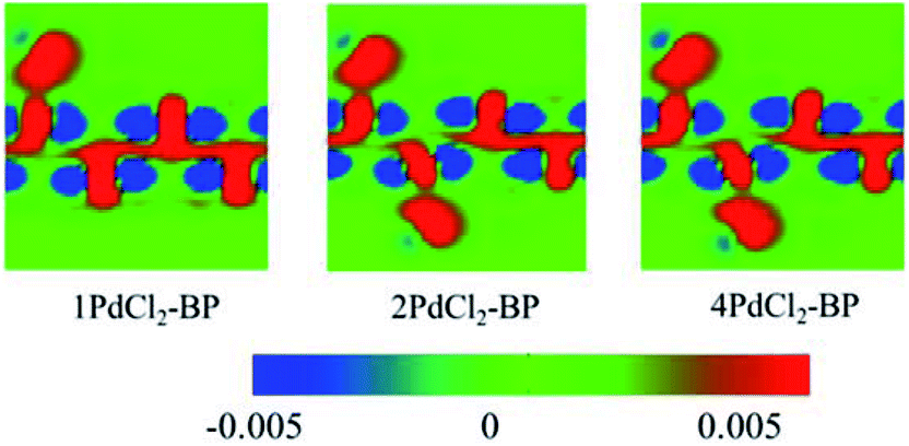 | ||
| Fig. 5 Computed electron difference densities of 1PdCl2-BP, 2PdCl2-BP, and 4PdCl2-BP. The green area means no electron transfer, red part represents obtaining electrons, while blue region indicates losing electrons. | ||
The nPdCl2-BP composites show p-type characteristics accompanied by the appearance of two kinds of midgap energy levels below the Ef (green and purple lines in Fig. 3 and 4). The higher one is close to the Ef and dominated by the Cl-3p state while the lower one is controlled by the Pd-4d state. The MLBP valence band is buried under the PdCl2 midgap energy levels and hybrids to some extent with Pd-4d/Cl-3p. Therefore, electrons can be transferred from the MLBP substrate to the PdCl2 quantum dots owing to the strong electronegativity of the Cl atom. The substrate MLBP and the appendant PdCl2 groups in nPdCl2-BP all contribute to the conduction band. The band gap values of MLBP in nPdCl2-BP do not bring much change relative to the pure MLBP, varying from 1.14 to 1.22 eV. However, the MLBP in nPdCl2-BP becomes to an indirect band gap semiconductor due to the orbital coupling of P with PdCl2, different from the direct feature in the pristine MLBP. In this case, the PdCl2 quantum dots play two-fold effects on the transport property. On one hand, they offer extra valence electrons to be excited to the conduction bands to participate in transporting which is beneficial for enhancing the conductivity. On the other hand, the electron excitation of PdCl2 midgap levels leaves holes for trapping electrons from MLBP, that is, PdCl2 quantum dots behave as additional scattering centers which degrade the mobility of the charge carriers. This is useful for devices which require fast switch off times.68 From the analysis above, it is concluded that the PdCl2 quantum dots exert an important effect in electron transporting, furthermore, such influence becomes more significant with the increasing grafting density n. This can be further confirmed by the calculated transport properties as addressed in the following section.
3.3 Transport property
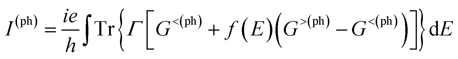
To compute the electron transport properties of MLBP and nPdCl2-BP (n = 1, 2, and 4), the two-probe devices were constructed by sandwiching a curved 2D structure (26.05 Å × 26.51 Å) of MLBP and nPdCl2-BP (n = 1, 2, and 4) between two Au electrodes as shown by Fig. 2. The current I through the scatter region was calculated based on the formula (1):57
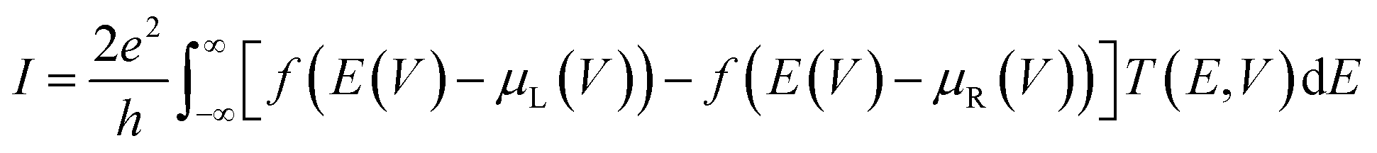 | (1) |
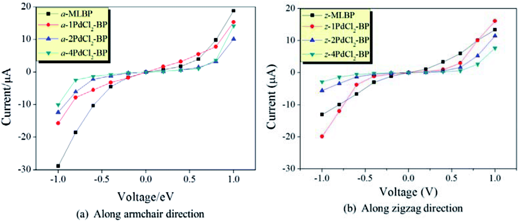
The transmissions along the armchair (a-nPdCl2-BP) and zigzag (z-nPdCl2-BP) directions are both considered. The calculated current–voltage (I–V) curves are given in Fig. 6. As for MLBP, electrons permeate easier through the armchair direction compared with the zigzag. For instance, at −1.0 V bias voltage, the current magnitude of a-MLBP is −28.88 μA, while it goes down to −13.03 μA in the z-MLBP device. This anisotropic phenomenon is still preserved after being pinned with PdCl2 quantum dots. For example, under −1.0 V bias voltage, a-4PdCl2-BP gives a current of −10.01 μA while z-4PdCl2-BP presents a lower data of −2.82 μA. It is noteworthy that grafting PdCl2 quantum dots to the MLBP surface could significantly influence the transport properties. On one hand, the conductivity is much lowered after anchoring PdCl2 quantum dots, and the current magnitudes at a certain bias voltage follow the sequence of MLBP > 1PdCl2-BP > 2PdCl2-BP > 4PdCl2-BP, indicating that the scatter effect of PdCl2 plays a major role in the process of electron transporting. On the other hand, the threshold voltage becomes more and more distinct with the increasing grafting density n. Pure MLBP shows continuously rising current from 0.2 to 1.0 V bias voltage, no evident threshold voltage is found. Turn to 4PdCl2-BP, off-state is kept until the applied bias reaches to ±0.8 V, on-state begins at ±1.0 V bias voltage. Prospectively, grafting MLBP with a large density of PdCl2 quantum dots paves a new way toward achieving electronic switch devices.
 | ||
| Fig. 6 Computed I–V curves for MLBP and nPdCl2-BP (n = 1, 2, and 4) two-probe devices. (a) Transport along the armchair direction, and (b) transport along the zigzag direction. | ||
To further shed light on effects of the PdCl2 grafting upon the transport properties, the transmission spectra (TS) for MLBP and nPdCl2-BP (n = 1, 2, and 4) at 1.0 V were calculated, as shown in Fig. 7. Usually, resonant peaks in the bias window contribute to the current. Here, the bias window refers to [–V/2, V/2]. Clearly, either for a-nPdCl2-BP device or for z-nPdCl2-BP device, the valence band resonant peaks (below the Ef) in the bias window shrink gradually with the growing number n, again indicating the trap effect of PdCl2 quantum dots. Evidently, the conduction band resonant peaks (above the Ef) in the bias window of a-nPdCl2-BP are much larger than those of z-nPdCl2-BP, and thereby the armchair direction gives a higher conductivity than the zigzag, in line with the I–V curves. These features can be further confirmed by the local density of state (LDOS) at the Ef (Fig. 8). Clearly, the LDOS of the scatter regions of both a-nPdCl2-BP and z-nPdCl2-BP fade away when adding more PdCl2 quantum dots, again indicating the block effect of PdCl2 quantum dots on electron transporting. Compared to a-nPdCl2-BP, the block phenomenon in z-nPdCl2-BP is more obvious, correlating well with the higher conductivity for the armchair direction as given by the I–V curves. We also calculated the real-space scattering states of the systems at the Ef for investigating the transport paths. Fourteen transport channels are obtained (cf. Fig. S1–S8 in ESI†), indicating that there exist fourteen subbands in the left electrode along the transport direction. Fig. 9 gives the most effective channels for MLBP and nPdCl2-BP (n = 1, 2, and 4). It can be seen that the transport channels tend to be closed if attaching more PdCl2 quantum dots due to their scattering effect, also intuitively explaining the reducing of the conductivity. Moreover, the penetrating channel of z-nPdCl2-BP is weaker at the right side than that of a-nPdCl2-BP, giving the evidence that charge carriers transport easily along the armchair direction related to the zigzag direction.
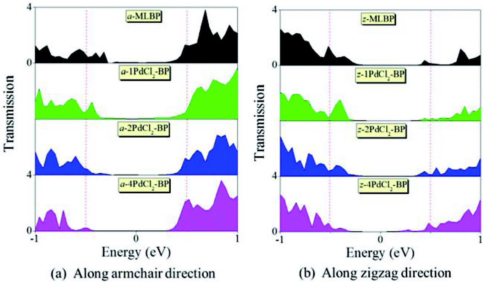 | ||
| Fig. 7 Transmission spectra of MLBP and nPdCl2-BP (n = 1, 2, and 4) two-probe devices at 1.0 V bias voltage. (a) Transport along the armchair direction, and (b) transport along the zigzag direction. Red dashed lines indicate the bias window. | ||
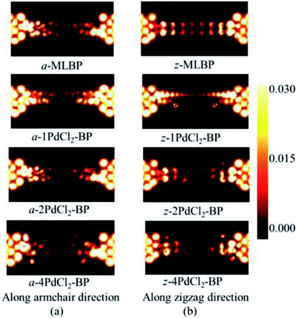 | ||
| Fig. 8 The computed LDOS at the Fermi level Ef for a-MLBP, z-MLBP, a-nPdCl2-BP, and z-nPdCl2-BP (n = 1, 2, and 4) two-probe devices at 1.0 V bias voltage. | ||
 | ||
| Fig. 9 The real space scattering states at Fermi energy Ef of a-MLBP, z-MLBP, a-nPdCl2-BP, and z-nPdCl2-BP (n = 1, 2, and 4) two-probe devices. | ||
3.4 Optoelectronic property
Fig. 2 schematically shows the structures of our devices of nPdCl2-BP (n = 1, 2, and 4) for calculating optoelectronic properties along the armchair and zigzag directions. A linear polarized light was irradiated on the whole scattering region. The applied light has a polarization forming an angle θ with respect to the transport direction of the MLBP plane. The photoresponses were determined at different θ for photon energies ranging from 0 to 1.0 eV with an interval of 0.1 eV. The photocurrent I(ph) can be obtained from the following formula (2):69
 | (2) |
The photocurrent of eqn (2) can be separated into three terms:70
 | (3) |
 | (4) |
Photoresponses along both armchair and zigzag directions of MLBP and nPdCl2-BP (n = 1, 2, and 4) at photo energies of 0.7, 0.8, and 1.0 eV are given in Fig. 10. According to formula (3), the photoresponses correlate directly to the sin2![[thin space (1/6-em)]](https://www.rsc.org/images/entities/char_2009.gif) θ, cos2θ, and sin2θ components. Therefore, the photoresponse curves in Fig. 10 take the sine or cosine shapes with θ, which are decided by complicated factors such as the geometric symmetry and band structures of the material. The sign of the photoresponse varies with θ and applied photon energy. This is due to the fact that the sign of the photoresponse is determined by the summation of all activated electrons with different velocity distributions. It is noteworthy that bonding PdCl2 quantum dots is much beneficial for enhancing photoresponses. Regardless of the direction, the maximum photoresponses within the considered photon energies are ordered as 4PdCl2-BP > 2PdCl2-BP > 1PdCl2-BP > MLBP. Values for a-4PdCl2-BP and z-4PdCl2-BP are up to 1.23 and 8.53 a02/photon, respectively, 22 and 15 times larger than that of a-MLBP (0.0546 a02/photon) and z-MLBP (0.579 a02/photon). This is due to the fact that electrons can be excited easily by the light from the PdCl2 quantum dots which can be demonstrated from the band structures aforementioned. Fig. 11 shows the variation of maximum photoresponses with photo energies. Evidently, the nPdCl2-BP (n = 1, 2, and 4) nanostructures have produced photoresponse anisotropy: zigzag direction is about one order of magnitude larger than armchair. All of these fascinating photoresponse properties make these new 2D materials especially attractive for optoelectronic devices.
θ, cos2θ, and sin2θ components. Therefore, the photoresponse curves in Fig. 10 take the sine or cosine shapes with θ, which are decided by complicated factors such as the geometric symmetry and band structures of the material. The sign of the photoresponse varies with θ and applied photon energy. This is due to the fact that the sign of the photoresponse is determined by the summation of all activated electrons with different velocity distributions. It is noteworthy that bonding PdCl2 quantum dots is much beneficial for enhancing photoresponses. Regardless of the direction, the maximum photoresponses within the considered photon energies are ordered as 4PdCl2-BP > 2PdCl2-BP > 1PdCl2-BP > MLBP. Values for a-4PdCl2-BP and z-4PdCl2-BP are up to 1.23 and 8.53 a02/photon, respectively, 22 and 15 times larger than that of a-MLBP (0.0546 a02/photon) and z-MLBP (0.579 a02/photon). This is due to the fact that electrons can be excited easily by the light from the PdCl2 quantum dots which can be demonstrated from the band structures aforementioned. Fig. 11 shows the variation of maximum photoresponses with photo energies. Evidently, the nPdCl2-BP (n = 1, 2, and 4) nanostructures have produced photoresponse anisotropy: zigzag direction is about one order of magnitude larger than armchair. All of these fascinating photoresponse properties make these new 2D materials especially attractive for optoelectronic devices.
 | ||
| Fig. 10 The calculated photoresponse R for MLBP and nPdCl2-BP (n = 1, 2, and 4) two-probe devices irradiated by linearly polarized light. (a) Photoresponse along the armchair direction, and (b) photoresponse along the zigzag direction. | ||
 | ||
| Fig. 11 The calculated maximum photoresponse R for a-MLBP, z-MLBP, a-nPdCl2-BP, and z-nPdCl2-BP (n = 1, 2, and 4) two-probe devices irradiated by linearly polarized light. | ||
4. Summary
Electronic, transport, and optoelectronic properties of MLBP and nPdCl2-BP (n = 1, 2, and 4) are examined by using DFT and NEGF as well as the KNEGF methods. It is found that the PdCl2 quantum dots prefer to locate over the furrow site of MLBP and form a planar quadridentate structure of . A typical Pd–P coordinate bond is formed. The PdCl2 quantum dots introduce discrete flat levels just above the MLBP valence band and below the Ef. The conductivity is much lowered by the PdCl2 grafting, due to the fact that the scatter effect of PdCl2 quantum dots play a major role in the process of electron transporting. For both parent MLBP and functioned nPdCl2-BP (n = 1, 2, and 4), the armchair direction shows higher conductivities than the zigzag. A threshold voltage is found for 4PdCl2-BP, a valuable clue for exploring current switches. More importantly, functionalization of PdCl2 quantum dots is much beneficial for enhancing photoresponse. Values of photoresponse for a-4PdCl2-BP and z-4PdCl2-BP are 22 and 15 times larger than that of a-MLBP and z-MLBP, respectively. A significant photoresponse anisotropy is found for both MLBP and nPdCl2-BP (n = 1, 2, and 4), contrary to the conductivity, the zigzag direction shows much stronger photoresponse than the armchair. All of the aforementioned unique properties make this new 2D MLBP based materials especially attractive for both electronic and optoelectronic devices.
Conflicts of interest
There are no conflicts to declare.Acknowledgements
This work was supported by National Natural Science Foundation of China (Grant No. 51473042), Nature Science Foundation of Heilongjiang Province of China (Grant No. B2018007), Harbin foundation for leaders of disciplines (Grant No. 2017RAXXJ002).References
- A. K. Geim and K. S. Novoselov, Nat. Mater., 2007, 6, 183–191 CrossRef CAS PubMed.
- G. Fiori, F. Bonaccorso, G. Iannaccone, T. Palacios, D. Neumaier, A. Seabaugh, S. K. Banerjee and L. Colombo, Nat. Nanotechnol., 2014, 7, 768–779 CrossRef PubMed.
- M. D. Stoller, S. Park, Y. Zhu, J. An and R. S. Ruoff, Nano Lett., 2008, 8, 3498–3502 CrossRef CAS PubMed.
- D. Voiry, J. Yang and M. Chhowalla, Adv. Mater., 2016, 28, 6197–6206 CrossRef CAS PubMed.
- A. H. Castro Neto, F. Guinea, N. M. R. Peres, K. S. Novoselov and A. K. Geim, Rev. Mod. Phys., 2009, 81, 109–162 CrossRef CAS.
- B. Radisavljevic, A. Radenovic, J. Brivio, V. Giacometti and A. Kis, Nat. Nanotechnol., 2011, 6, 147–150 CrossRef CAS PubMed.
- Y. Jing, X. Zhang and Z. Zhou, WIREs Computational Molecular Science, 2016, 6, 5–19 CrossRef CAS.
- P. Yasaei, B. Kumar, T. Foroozan, C. Wang, M. Asadi, D. Tuschel, J. E. Indacochea, R. F. Klie and A. Salehi-Khojin, Adv. Mater., 2015, 27, 1887–1892 CrossRef CAS PubMed.
- J. Kang, J. D. Wood, S. A. Wells, J. H. Lee, X. Liu, K. S. Chen and M. C. Hersam, ACS Nano, 2015, 9, 3596–3604 CrossRef CAS PubMed.
- Y. Zhang, N. Dong, H. Tao, C. Yan, J. Huang, T. Liu, A. W. Robertson, J. Texter, J. Wang and Z. Sun, Chem. Mater., 2017, 29, 6445–6456 CrossRef CAS.
- W. Zhao, Z. Xue, J. Wang, X. Zhao and T. Mu, ACS Appl. Mater. Interfaces, 2015, 7, 27608–27612 CrossRef CAS PubMed.
- A. H. Woomer, T. W. Farnsworth, J. Hu, R. A. Wells, C. L. Donley and S. C. Warren, ACS Nano, 2015, 9, 8869–8884 CrossRef CAS PubMed.
- W. Lu, H. Nan, J. Hong, Y. Chen, C. Zhu, Z. Liang, X. Ma, Z. Ni, C. Jin and Z. Zhang, Nano Res., 2014, 7, 853–859 CrossRef CAS.
- H. Kwon, S. W. Seo, T. G. Kim, E. S. Lee, P. T. Lanh, S. Yang, S. Ryu and J. W. Kim, ACS Nano, 2016, 10, 8723–8731 CrossRef CAS PubMed.
- M. Fortin-Deschênes, P. L. Levesque, R. Martel and O. Moutanabbir, J. Phys. Chem. Lett., 2016, 7, 1667–1674 CrossRef PubMed.
- Y. Chen, G. Jiang, S. Chen, Z. Guo, X. Yu, C. Zhao, H. Zhang, Q. Bao, S. Wen, D. Tang and D. Fan, Opt. Express, 2015, 23, 12823–12833 CrossRef CAS PubMed.
- L. Li, Y. Yu, G. J. Ye, Q. Ge, X. Ou, H. Wu, D. Feng, X. H. Chen and Y. Zhang, Nat. Nanotechnol., 2014, 9, 372–377 CrossRef CAS PubMed.
- S. Das, W. Zhang, M. Demarteau, A. Hoffmann, M. Dubey and A. Roelofs, Nano Lett., 2014, 14, 5733–5739 CrossRef CAS PubMed.
- J. Qiao, X. Kong, Z. X. Hu, F. Yang and W. Ji, Nat. Commun., 2014, 5, 4475 CrossRef CAS PubMed.
- F. Xia, H. Wang and Y. Jia, Nat. Commun., 2014, 5, 4458 CrossRef CAS PubMed.
- A. Castellanos-Gomez, J. Phys. Chem. Lett., 2015, 6, 4280–4291 CrossRef CAS PubMed.
- J. S. Kim, Y. Liu, W. Zhu, S. Kim, D. Wu, L. Tao, A. Dodabalapur, K. Lai and D. Akinwande, Sci. Rep., 2015, 5, 8989 CrossRef CAS PubMed.
- J. Pei, G. Xin, J. Yang, X. Wang, Z. Yu, D. Y. Choi, L. D. Barry and Y. Lu, Nat. Commun., 2016, 7, 10450 CrossRef CAS PubMed.
- D. Yuchen, L. Han, D. Yexin and D. Y. Peide, ACS Nano, 2014, 8, 10035–10042 CrossRef PubMed.
- L. Li, M. Engel, D. B. Farmer, S. J. Han and H. S. P. Wong, ACS Nano, 2016, 10, 4672–4677 CrossRef CAS PubMed.
- K. Gong, L. Zhang, W. Ji and H. Guo, Phys. Rev. B: Condens. Matter Mater. Phys., 2014, 90, 125441 CrossRef.
- Y. Ma, C. Shen, A. Zhang, L. Chen, Y. Liu, J. Chen, Q. Liu, Z. Li, M. R. Amer, T. Nilges, A. N. Abbas and C. Zhou, ACS Nano, 2017, 11, 7126–7133 CrossRef CAS PubMed.
- C. Han, Z. Hu, L. C. Gomes, Y. Bao, A. Carvalho, S. J. R. Tan, B. Lei, D. Xiang, J. Wu, D. Qi, L. Wang, F. Huo, W. Huang, K. P. Loh and W. Chen, Nano Lett., 2017, 17, 4122–4129 CrossRef CAS PubMed.
- Q. F. Li, X. G. Wan, C. G. Duan and J. L. Kuo, J. Phys. D: Appl. Phys., 2014, 47, 465302 CrossRef.
- X. Y. Tan, J. H. Wang, Y. Y. Zhu, Y. Zuo and X. Jin, Acta Phys. Sin., 2014, 63, 207301 Search PubMed.
- S. Zhao, W. Kang and J. Xue, J. Mater. Chem. A, 2014, 2, 19046–19052 RSC.
- G. L. Xu, Z. Chen, G. M. Zhong, Y. Liu, Y. Yang, T. Ma, Y. Ren, X. Zuo, X. H. Wu, X. Zhang and K. Amine, Nano Lett., 2016, 16, 3955–3965 CrossRef CAS PubMed.
- G. C. Constantinescu and N. D. Hine, Nano Lett., 2016, 16, 2586–2594 CrossRef CAS PubMed.
- R. A. Doganov, S. P. Koenig, Y. Yeo, K. Watanabe, T. Taniguchi and B. Ozyilmaz, Appl. Phys. Lett., 2015, 106, 083505 CrossRef.
- P. Zhang, J. Wang and X. M. Duan, Chin. Phys. B, 2016, 25, 037302 CrossRef.
- Y. Deng, Z. Luo, N. J Conrad, H. Liu, Y. Gong, S. Najmaei, P. M. Ajayan, J. Lou, X. Xu and P. D. Ye, ACS Nano, 2014, 8, 8292–8299 CrossRef CAS PubMed.
- L. Ye, H. Li, Z. Chen and J. Xu, ACS Photonics, 2016, 3, 692–699 CrossRef CAS.
- V. Kumar, J. R. Brent, M. Shorie, H. Kaur, G. Chadha, A. G. Thomas, E. A. Lewis, A. P. Rooney, L. Nguyen, X. Zhong, M. G. Burke, S. J. Haigh, A. Walton, P. D. Mcnaughter, A. A. Tedstone, N. Savjani, C. A. Muryn, P. O'Brien, A. K. Ganguli, D. J. Lewis and P. Sabherwal, ACS Appl. Mater. Interfaces, 2016, 8, 22860–22868 CrossRef CAS PubMed.
- Q. Li, Q. Zhou, X. Niu, Y. Zhao, Q. Chen and J. Wang, J. Phys. Chem. Lett., 2016, 7, 4540–4546 CrossRef CAS PubMed.
- S. P. Koenig, R. A. Doganov, L. Seixas, A. Carvalho, J. Y. Tan, K. Watanabe, T. Taniguchi, N. Yakovlev, A. H. Castro Neto and B. Özyilmaz, Nano Lett., 2016, 16, 2145–2551 CrossRef CAS PubMed.
- V. V. Kulish, O. I. Malyi, C. Persson and P. Wu, Phys. Chem. Chem. Phys., 2015, 17, 992–1000 RSC.
- T. Hu and J. Hong, J. Phys. Chem. C, 2015, 119, 8199–8207 CrossRef CAS.
- N. Suvansinpan, F. Hussain, G. Zhang, C. H. Chiu, Y. Cai and Y. W. Zhang, Nanotechnology, 2016, 27, 065708 CrossRef PubMed.
- W. Lei, T. Zhang, P. Liu, A. R. Jose, G. Liu and M. Liu, ACS Catal., 2016, 6, 8009–8020 CrossRef CAS.
- Y. Zhao, H. Wang, H. Huang, Q. Xiao, Y. Xu, Z. Guo, H. Xie, J. Shao, Z. Sun, W. Han, X. F. Yu, P. Li and P. K. Chu, Angew. Chem., Int. Ed., 2016, 55, 5003–5007 CrossRef CAS PubMed.
- E. Alonso, J. Forniés, C. Fortuño, A. Lledós, A. Martín and A. Nova, Inorg. Chem., 2009, 48, 7679–7690 CrossRef CAS PubMed.
- V. I. Bakhmutov, F. Bozoglian, K. Gómez, G. González, V. V. Grushin, S. A. Macgregor, E. Martin, F. M. Miloserdov, M. A. Novikov, J. A. Panetier and L. V. Romashov, Organometallics, 2011, 31, 1315–1328 CrossRef.
- D. E. Berry, P. Carrie, K. L. Fawkes, B. Rebner and Y. Xing, J. Chem. Educ., 2010, 87, 533–534 CrossRef CAS.
- L. R. Moore, E. C. Western, R. Craciun, J. M. Spruell and D. A. Dixon, Organometallics, 2008, 27, 576–593 CrossRef CAS.
- K. Herbst, P. Zanello, M. Corsini, N. D. Amelio, L. Dahleburg and M. Brorson, Inorg. Chem., 2003, 42, 974–981 CrossRef CAS PubMed.
- J. C. W. Folmer, J. A. Turner and B. A. Parkinson, J. Solid State Chem., 1987, 68, 28–37 CrossRef CAS.
- V. Tran, R. Soklaski, Y. Liang and L. Yang, Phys. Rev. B: Condens. Matter Mater. Phys., 2014, 89, 235319 CrossRef.
- Y. Du, J. Maassen, W. Wu, Z. Luo, X. Xu and P. D. Ye, Nano Lett., 2016, 16, 6701–6708 CrossRef CAS PubMed.
- R. Fei and L. Yang, Nano Lett., 2014, 14, 2884–2889 CrossRef CAS PubMed.
- J. P. Perdew, K. Burke and M. Ernzerhof, Phys. Rev. Lett., 1996, 77, 3865–3868 CrossRef CAS PubMed.
- M. Brandbyge, J. L. Mozos, P. Ordejon, J. Taylor and K. Stokbro, Phys. Rev. B: Condens. Matter Mater. Phys., 2002, 65, 165401 CrossRef.
- J. M. Soler, E. Artacho, J. D. Gale, A. Garcia, J. Junquera, P. Ordejon and D. Sanchez-Portal, J. Phys.: Condens. Matter, 2002, 14, 2745–2779 CrossRef CAS.
- ATK, Version 13.8, atomistix a/s, 2013, www.quantumwise.com Search PubMed.
- S. Å. Gustafson and G. Dahlquist, Chem. Phys. Lett., 2011, 508, 215–218 CrossRef.
- J. Taylor, H. Guo and J. Wang, Phys. Rev. B: Condens. Matter Mater. Phys., 2001, 63, 245407 CrossRef.
- D. Waldron, P. Haney, B. Larade, A. MacDonald and H. Guo, Phys. Rev. Lett., 2006, 96, 166804 CrossRef PubMed.
- T. Takahashi, H. Tokailin, S. Suzuki and I. Shirotani, J. Phys. C: Solid State Phys., 1985, 18, 825–836 CrossRef CAS.
- M. A. Carvajal, G. P. Miscione, J. J. Novoa and A. Bottoni, Organometallics, 2005, 24, 2086–2096 CrossRef CAS.
- H. Liu, A. T. Neal, Z. Zhu, Z. Luo, X. Xu, D. Tomanek and P. D. Ye, ACS Nano, 2014, 8, 4033–4041 CrossRef CAS PubMed.
- S. Das, W. Zhang, M. Demarteau, A. Hoffmann, M. Dubey and A. Roelofs, Nano Lett., 2014, 14, 5733–5739 CrossRef CAS PubMed.
- Y. Du, C. Ouyang, S. Shi and M. Lei, J. Appl. Phys., 2010, 107, 093718 CrossRef.
- T. H. Oosterkamp, T. Fujisawa, W. G. V. D. Wiel, K. Ishibashi, R. V. Hijman, S. Tarucha and L. P. Kouwenhoven, Nature, 1998, 395, 873–876 CrossRef CAS.
- B. G. Streetman and S. K. Banerjee, Solid State Electronic Devices, Sixth Edition, Prentice Hall, 2006 Search PubMed.
- L. Zhang, K. Gong, J. Chen, L. Liu, D. Xiao and H. Guo, Phys. Rev. B: Condens. Matter Mater. Phys., 2014, 90, 195428 CrossRef.
- Y. Xie, L. Zhang, Y. Zhu, L. Liu and H. Guo, Nanotechnology, 2015, 26, 455202 CrossRef PubMed.
Footnote |
| † Electronic supplementary information (ESI) available. See DOI: 10.1039/c8ra07053a |
| This journal is © The Royal Society of Chemistry 2018 |