
 Open Access Article
 This Open Access Article is licensed under a Creative Commons Attribution-Non Commercial 3.0 Unported Licence
Improvement in interlayer structure of p–i–n-type organic solar cells with the use of fullerene-linked tetrabenzoporphyrin as additive†
Yuto Tamuraa,
Mitsuharu Suzuki a,
Takaki Nakagawab,
Tomoyuki Koganezawac,
Sadahiro Masuob,
Hironobu Hayashia,
Naoki Aratania and
Hiroko Yamada*a
a,
Takaki Nakagawab,
Tomoyuki Koganezawac,
Sadahiro Masuob,
Hironobu Hayashia,
Naoki Aratania and
Hiroko Yamada*a
aDivision of Materials Science, Graduate School of Science and Technology, Nara Institute of Science and Technology, 8916-5 Takayama-cho, Ikoma, Nara 630-0192, Japan. E-mail: hyamada@ms.naist.jp
bDepartment of Applied Chemistry and Environment, Kwansei Gakuin University, 2-1 Gakuen, Sanda, Hyogo 669-1337, Japan
cJapan Synchrotron Radiation Research Institute, 1-1-1 Kouto, Sayo-cho, Sayo-gun, Hyogo 679-5198, Japan
First published on 15th October 2018
Abstract
The additive effect on small-molecule-based p–i–n-type devices has been little investigated so far. We focus on the improvement of the miscibility of tetrabenzoporphyrin (BP) and [6,6]-phenyl-C61-butyric acid methyl ester (PC61BM) blend film by addition of fullerene-linked tetrabenzoporphyrin (BP–C60) as an additive to the interlayer (i-layer). BP is one of the most promising p-type organic semiconductors, and BP films can be prepared readily by heating as-cast films of the precursor (a bicyclo[2.2.2]octadiene-fused porphyrin; CP), that results in changes from amorphous CP films to polycrystalline BP films. Because of the high crystallinity of BP, large BP grains on the scale of tens to hundreds of nanometers are generated in blend films of BP and PC61BM during film fabrication. We found that the addition of BP–C60 as an additive (3, 5, 7, and 10 wt%) to the i-layer composed of BP and PC61BM improves the miscibility of BP and PC61BM. The power conversion efficiency of p–i–n-type organic solar cells consisting of a blend film of BP and PC61BM (i-layer) sandwiched by BP (p-layer) and PC61BM (n-layer) improved by up to 50% as compared to that of a control device after the addition of BP–C60 to the i-layer. The film morphology was investigated using atomic force microscopy, fluorescence microspectroscopy, two-dimensional grazing-incident wide-angle X-ray diffraction measurements, and scanning electron microscopy. Interacting with both BP and PC61BM, the addition of BP–C60 led to changes in the grain size as well as an increase in the size of the BP/PC61BM interface and hence effective charge separation in the p–i–n device. This morphological improvement is attributable to the ability of BP–C60, which exhibits the characteristics of both BP and C60, to promote the compatibility of BP and PC61BM. This study is a significant step towards the development of high-performance p–i–n-type solar cells and should pave the way for the fabrication of high-performance bulk-heterojunction layers in solution-processed organic photovoltaic devices.
Introduction
Solution-processed organic solar cells (OSCs) are attracting increasing attention because of their unique properties, such as lightweight and flexible nature, as well as the fact that they can be fabricated by low-cost techniques such as roll-to-roll processing.1–5 During the past decade, the power conversion efficiency (PCE) of lab-scale OSCs has shown rapid increases because of the synergic evolution of photovoltaic materials (both p-type and n-type)6–13 and device structures.14,15 In addition to the developments of the materials and device structure, the optimization of the active layer structure is essential for ensuring the highest PCE in almost all cases. The bulk-heterojunction (BHJ)-type active layer, in which p-type and n-type materials are blended, has shown great promise for use in high-efficiency OSCs.16,17 The two blended components form a large-area p–n junction, where exciton dissociation occurs at the interface. Further, the bi-continuous phases allow the ready hole and electron transport toward the respective electrodes. As a result, OSCs based on the BHJ continue to exhibit the highest PCE values of approximately 10–12%18–25 and are the most widely studied OSCs. On the other hand, controlling the three-dimensional nanomorphology with the aim of optimizing the BHJ film remains a challenge. To date, several strategies have been suggested for ensuring this aim. They include the use of different processing solvents26 and solvent additives27–29 as well as thermal,30–34 and solvent annealing.34–42 However, these strategies depend to a great extent on the properties of p- and n-type materials such as its solubility, crystallinity, and miscibility. The orientation of the molecules on the substrate and in active layer is also important.The precursor approach is one of the most suitable methods for constructing effective active layers through a solution-based process. In this approach, highly soluble and non-aggregating precursor molecules of the target semiconductor materials are deposited on the substrate by a solution-based process and then converted in situ into the target material through thermal stimulation or photostimulation.43–52 Since the conversion of the precursor into the semiconducting material involves a decrease in the solubility owing to the induced structural changes, a three-layered p–i–n structure with the above-mentioned vertical-phase separation can be achieved through solution-based processes.53–57 Here, “i” stands for the interlayer between the p- and n-layers. Similar to the BHJ film, this layer consists of blended p- and n-type materials.
Tetrabenzoporphyrin (BP), which exhibits superior p-type semiconductor characteristics, is one of the most successful materials for the thermal precursor approach to construct p–i–n devices. The precursor of BP, a bicyclo[2.2.2]octadiene-fused porphyrin (CP),56 is solution processable, and the obtained film can be transformed into a polycrystalline BP film by thermal annealing (Fig. 1). Matsuo and co-workers successfully demonstrated the interdigitated structure in a p–i–n device through this thermal precursor approach using BP and bis(dimethylphenylsilylmethyl)[60]fullerene, with the device exhibiting good performance.54 In addition, Nguyen and co-workers investigated the nanoscale morphology of a p–i–n device based on BP and either [6,6]-phenyl-C61-butyric acid methyl ester (PC61BM) or [6,6]-phenyl-C61-butyric acid n-butyl ester.55 Thus, there have been several reports on controlling the morphology during the thermal precursor approach using well-studied fullerene derivatives. On the other hand, there have been few studies on other strategies for modifying the structure of the i-layer during the thermal precursor approach. This is probably due to the difficulty in inducing morphological changes in the robust BP film through additional annealing processes or by using solvent additives.
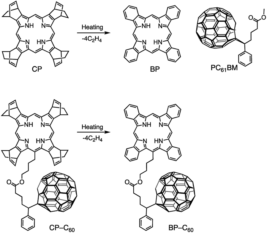 | ||
| Fig. 1 Chemical transformation of CP into BP and CP–C60 into BP–C60 through heating and chemical structure of PC61BM. | ||
Several groups have explored the possibility of using fullerene-linked molecular additives for tuning the morphology of poly(3-hexylthiophene) (P3HT):PC61BM BHJ devices. A graft-block-type copolymer,58 block copolymer,59–61 fullerene-end capped P3HT,62 fullerene-linked oligothiophene,63,64 and pyrene-capped PC61BM65 have been used as additives for this purpose. Since fullerene-linked materials can be preferentially placed at the interface between two distinct heterophased materials, the successful incorporation of these materials improves device performance by reducing the P3HT and/or PC61BM domain size and suppressing micrometer-sized separation. Further, the use of these additives also improves device storage stability. Thus, despite the significant differences in the chemical structures and properties of these additives, their addition has an undeniably positive effect on the device characteristics.
In the case of small-molecule-based p–i–n-type devices, the additive effect has not been investigated extensively, because intact crystalline blend films of BP and PC61BM tend to exhibit good storage stability without additives. However, these materials show poor miscibility also because of the high crystallinity. The discovery of a suitable additive to improvethe miscibility of BP and PC61BM would significantly increase the PCE of BP:PC61BM OSCs because of the efficient charge separation. Recently, we reported a fullerene-linked BP (BP–C60) molecule as an OSC material based on the precursor approach using corresponding CP-type precursor (CP–C60), which can be quantitatively converted to BP–C60 by heating (Fig. 1). We systematically investigated the effect of covalent linkage between the BP (p-material) and C60 (n-material) units on the performance of solution-processed BHJ and p–i–n devices as well as the optical properties in solution.66,67 Based on the studies on BP–C60, we expected BP–C60 to be highly suitable for use as an additive of BP and PC61BM blend films because of the following reasons: (1) BP–C60 exhibited effective intramolecular electron transfer between BP and C60 in CH2Cl2. This result suggests that the addition of BP–C60 to BP:PC61BM films would promote the effective charge generation. Devices based on BP–C60 films showed better photovoltaic performance as compared to that of devices based on blended 1![[thin space (1/6-em)]](https://www.rsc.org/images/entities/char_2009.gif) :1 BP:PC61BM films in the same conditions;67 (2) crystallization does not occur during the thermal conversion of CP–C60 into BP–C60 at 160–220 °C (Fig. S1, ESI†) and BP–C60 itself exhibits high homogeneity in film form and thus forms amorphous films; (3) because the additive is constructed with the same components with the p- and n-materials, it is well miscible in i-layer. The addition of BP–C60 to BP:PC61BM films would inhibit the aggregation of BP to some extent, but each of BP and C60 in BP–C60 tend to gather BP and PC61BM, respectively, because of their crystallinity. Therefore the smaller domains will be obtained by adding the additive. Thus, an improvement in the PCE with addition of BP–C60 is expected.
:1 BP:PC61BM films in the same conditions;67 (2) crystallization does not occur during the thermal conversion of CP–C60 into BP–C60 at 160–220 °C (Fig. S1, ESI†) and BP–C60 itself exhibits high homogeneity in film form and thus forms amorphous films; (3) because the additive is constructed with the same components with the p- and n-materials, it is well miscible in i-layer. The addition of BP–C60 to BP:PC61BM films would inhibit the aggregation of BP to some extent, but each of BP and C60 in BP–C60 tend to gather BP and PC61BM, respectively, because of their crystallinity. Therefore the smaller domains will be obtained by adding the additive. Thus, an improvement in the PCE with addition of BP–C60 is expected.
With these facts in mind, in this study, we demonstrate an effective approach for morphological control using BP–C60 as an additive for BP:PC61BM-based p–i–n devices. The experimental results showed that, when added to the i-layer, BP–C60 is compatible with both BP and PC61BM and helps improve the film structure. After the addition of 5 wt% BP–C60 to the i-layer, the PCE of the resulting p–i–n device increased by up to50% with respect to that of a control p–i–n device. The fabricated films were investigated in detail using atomic force microscopy (AFM), fluorescence microspectroscopy, two-dimensional grazing-incident wide-angle X-ray diffraction (2D-GIWAXD) measurements, and scanning electron microscopy (SEM).
Results and discussion
To begin with, the effect of BP–C60 as a morphological additive for the internal BP:PC61BM layer in p–i–n devices was investigated. The p–i–n devices were prepared as shown in Fig. 2 (see Experimental for more details). The BP film for the p-layer was prepared on a (3,4-ethylenedioxythiophene):poly(4-styrenesulfonate) (PEDOT:PSS)-coated indium-tin-oxide (ITO) substrate by the spin-coating of CP followed by heating (thermal precursor approach). In the same manner, i-layers containing BP:PC61BM with and without BP–C60 were prepared on the BP film by the spin-coating of a CP:PC61BM solution with and without CP–C60 followed by heating. The obtained p–i-structure is labelled as Structure I. The n-layer of PC61BM was deposited on Structure I by spin-coating a PC61BM solution and subsequent thermal annealing. Finally, the buffer and metal electrode were deposited on the n-layer to form the p–i–n devices, which contained different amounts of BP–C60. For microscopic observations of the BP structure on the p-layer, Structure I was rinsed by using a drop of chloroform on the substrate and subjecting it to spinning, then Structure II was obtained. The photovoltaic performances of the various p–i–n devices are listed in Table 1 and Fig. 3a. After the addition of BP–C60 to the BP:PC61BM i-layer, the photovoltaic performance of the p–i–n devices was significantly enhanced.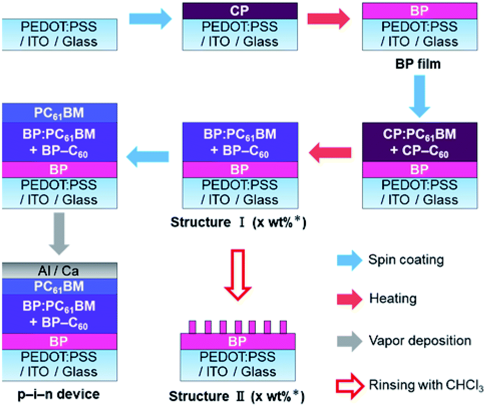 | ||
| Fig. 2 Procedure of device fabrication (* amount of BP–C60 added was 0–10 wt%). | ||
| BP–C60/wt% | i-layer thickness/nm | PCEb/% (PCEavec/%) | JSCb/mA cm−2 | VOCb/V | FFb | Rsb/Ω cm2 | Rshb,d/Ω cm2 | μh/10−4 cm2 V−1 s−1 (active-layer thickness/nm) | μe/10−4 cm2 V−1 s−1 (active-layer thickness/nm) |
|---|---|---|---|---|---|---|---|---|---|
| a Obtained under AM1.5G illumination at 100 mW cm−2.b Parameters of the best-performing cells.c Averages and standard deviations of four devices.d Rs: series resistance; Rsh: shunt resistance. | |||||||||
| 0 | 65 | 1.58 (1.4 ± 0.1) | 5.93 | 0.50 | 0.53 | 7 | 383 | 1.0 (109) | 0.9 (103) |
| 3 | 63 | 2.10 (2.02 ± 0.06) | 6.29 | 0.56 | 0.60 | 10 | 795 | 2.0 (145) | 2.1 (140) |
| 5 | 67 | 2.38 (2.30 ± 0.08) | 6.76 | 0.58 | 0.61 | 9 | 795 | 2.3 (138) | 2.9 (129) |
| 7 | 60 | 2.22 (2.12 ± 0.08) | 6.91 | 0.56 | 0.58 | 9 | 600 | 1.6 (140) | 2.7 (138) |
| 10 | 64 | 2.18 (2.10 ± 0.06) | 6.65 | 0.57 | 0.58 | 9 | 769 | 2.0 (130) | 1.4 (148) |
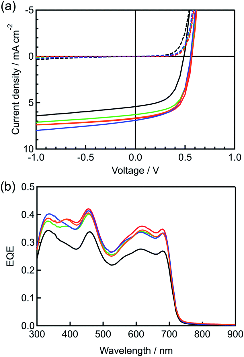 | ||
| Fig. 3 Photovoltaic performances of the best devices fabricated using different amounts of BP–C60: (a) illuminated (solid line) and dark (dotted line) J–V characteristics and (b) EQE spectra. 0 wt%: black; 3 wt%: green; 5 wt%: red; 7 wt%: blue; and 10 wt%: orange lines. | ||
For instance, the JSC, VOC, and FF values were improved with an increase in the amount of the added BP–C60 from 0 to 3 and 5 wt%, leading to increases in the PCE from 1.58 to 2.10 and 2.38%, respectively. On the other hand, when more than 7 wt% of BP–C60 was added, the PCE value decreased slightly, to 2.22 and 2.18% at 7 and 10 wt%, respectively. It should be noted that the thickness of the i-layer barely changed, suggesting that the presence of BP–C60 in the i-layer was responsible for the observed changes in the device performance. To elucidate the reason for the higher JSC values of the BP–C60-containing p–i–n devices, their external quantum efficiency (EQE) spectra were measured and compared with that of the control p–i–n device (0 wt%), as shown in Fig. 3b. The BP–C60-containing devices showed higher EQE values for wavelengths of 340 nm, 400–500 nm, and 550–720 nm, even though the active layers in all the devices had the same photoabsorption capability (see Fig. S2, ESI†). Further, the p–i–n devices (3–10 wt%) show improved EQE values within the photoabsorption range of the BP:PC61BM blend as compared to that of the 0 wt% device. For example, the best-performing p–i–n device(5 wt%) exhibited quantum efficiencies that were 13%, 25%, and 30% higher than those of the 0 wt% device at 340, 455, and 615 nm, respectively. The charge transport ability of the films was evaluated by space-charge-limited current (SCLC) measurement, as shown in Table 1. Both of hole and electron mobilities (μh and μe, respectively) of active layers are two to three times improved by addition of additives. These improvements can be attributed to the effective carrier generation at the p–n interface area enlarged by addition of BP–C60.
To investigate the microscopic surface morphology of the i-layer, the Structure I of the various samples was investigated using AFM, as shown in Fig. 4a–e. Several grains can be seen on the film in all the AFM images. These grains are attributable to BP-rich domains. Nguyen et al. also reported similar grains on the surfaces of BP/BP:PC61BM films and, based on conductive and photoconductive AFM measurements, characterized these grains as being BP-rich domains.55 In the case of Structure I (0 wt%), 1–2 μm-sized spot- and needle-like domains were observed, with the root-mean-square (RMS) surface roughness of the i-layer being 48.6 nm. This inhomogeneous distribution of the BP and PC61BM components is undesirable from the viewpoint of the photovoltaic process and was probably the reason this device exhibited the lowest PCE (1.58%) as well as a low FF value (0.53). On the other hand, the Structure I corresponding to the 3–10 wt% BP–C60 devices were significantly smoother, with the markedly lower RMS roughness values at 33.5 nm (3 wt%), 12.0 nm (5 wt%), 20.5 nm (7 wt%), and 6.4 nm (10 wt%). In p–i–n devices based on BP:fullerene derivatives, the flatness of the i-layer plays a critical role in ensuring a homogeneous morphology of the n-layer required for improved performance.55,66,67 This is because large, vertically oriented BP grains often extend through the n-layer, and PC61BM-uncovered BP features are formed on the n-layer and reach the electrode. In fact, the shunt resistances (Rsh) in the p–i–n (3–10 wt%) devices with a flat n-layer were twice as high as that of the p–i–n (0 wt%) device (see Fig. S3, ESI†). In general, VOC increases with an increase in the Rsh. Thus, the slight improvement in VOC seen in the cases of the p–i–n (3–10 wt%) devices can be ascribed to these structural differences between the i- and n-layers. Furthermore, needle-like grains that gradually became smaller with an increase in the BP–C60 content were also observed. For instance, needle-like grains with a length of approximately 2 μm were present in the Structure I (3 and 5 wt%), whereas grains approximately 1 μm or smaller were seen in the Structure I (7 and 10 wt%). Considering that the typical exciton diffusion length in molecular organic materials is in the order of a few to tens of nanometers,68 the grains placed in parallel on the substrates in all the films were too long to allow for efficient charge separation. However, the smoother surface and smaller grains observed in Structure I in the cases of the p–i–n (3–10 wt%) devices were more effective than those of control device Structure I (0 wt%).
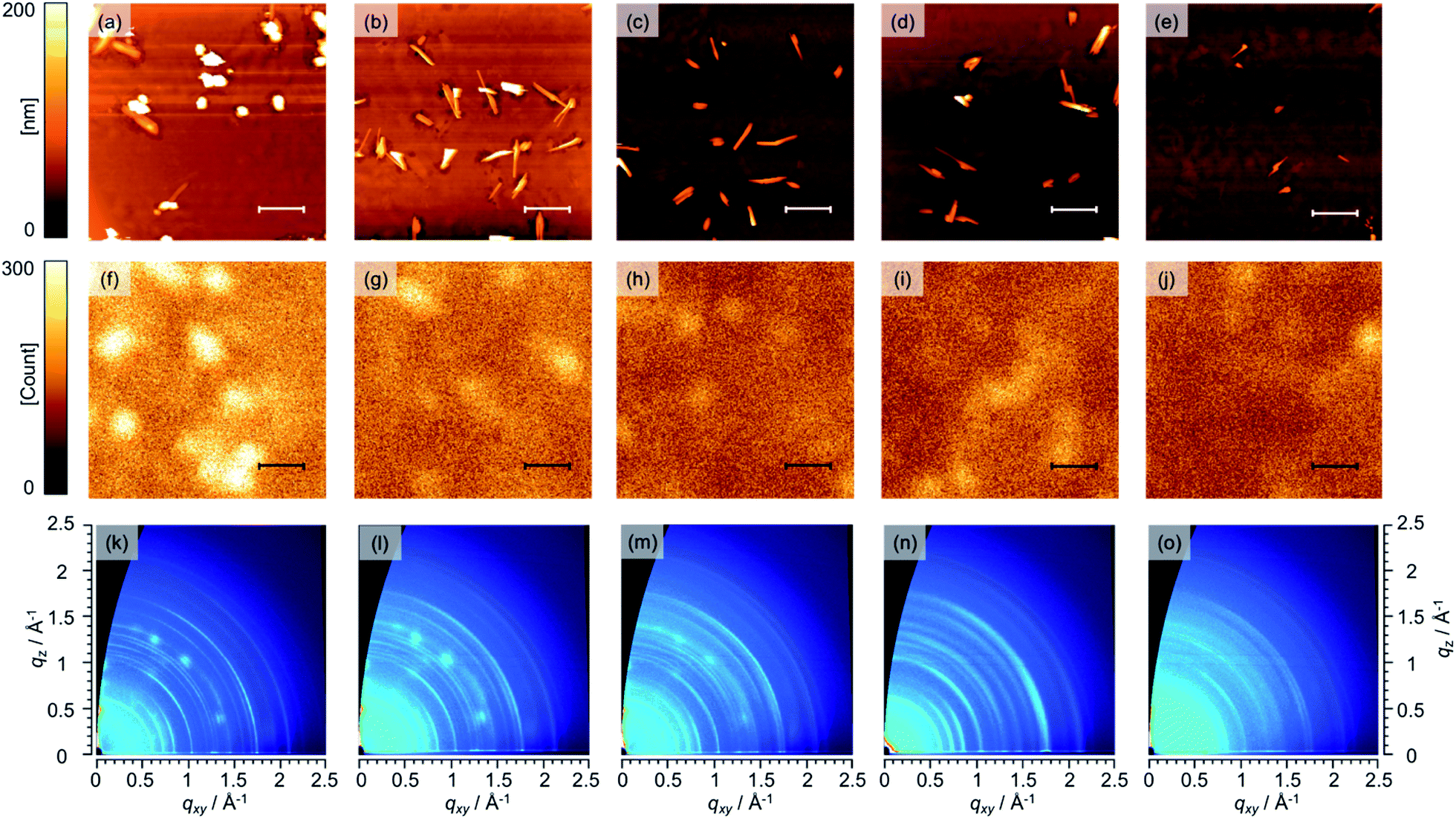 | ||
| Fig. 4 AFM hight images (top), fluorescence microspectroscopy images* (middle), and 2D-GIWAXD patterns (bottom) of Structure I surfaces corresponding to different amounts of BP–C60: (a), (f), and (k) 0 wt%; (b), (g), and (l) 3 wt%; (c), (h), and (m) 5 wt%; (d), (i), and (n) 7 wt%; and (e), (j), and (o) 10 wt%. Scale bars correspond to 2 μm. *To detect fluorescence of BP, 405 nm laser was used as excitation source. | ||
Further investigations of the macrostructure of Structure I were performed using fluorescence microspectroscopy. As shown in Fig. 4f–j, the intensity of the fluorescence from BP decreased gradually as the proportion of BP–C60 in the i-layer was increased. These data confirmed that the addition of BP–C60 led to more effective quenching of excitons in the BP domains, thus improving the characteristics of the BP:PC61BM interface with respect to the generation of hole–electron pairs. In addition, the numerous bright spots observed in the control device Structure I (0 wt%) were absent from the Structure I samples containing BP–C60. This suggests that more homogeneous BP:PC61BM films were formed after the addition of BP–C60.
The crystallinity and molecular orientation of Structure I were investigated through 2D-GIWAXD measurements. The obtained diffraction patterns are shown in Fig. 4k–o. The 2D-GIWAXD patterns confirmed that the BP in Structure I was polycrystalline with a monoclinic unit cell having the P21/n space group, as also reported by Aramaki et al.69 Further, the GIWAXD patterns of BP films have also been reported previously by Chabinyc et al.70 The GIWAXD patterns of BP in all the Structure I samples were similar. Note that the arcs of the (101) and (200) planes of BP, which had the highest intensity, were observed at qxy = 0.71 and 0.82 Å−1, respectively. Further, because the (101) and (200) planes, their appearance along the qxy axis suggested that vertically oriented herring-bone-like columns of BP were present on the substrate, resulting in improved hole transport, as described in Fig. S5, ESI.† From these results, it can be concluded that the presence of BP–C60 in the i-layer does not result in any changes in the orientation of the BP crystals. On the other hand, the crystallinity of BP decreased with the addition of a greater amount of BP–C60, since the full width at half maximum values of the (101) and (200) peaks as estimated by 1D vertical line cuts from 2D-GIWAXD data in the in-plane direction increased with an increase in the BP–C60 concentration (see Fig. S4, ESI†). In addition, GIWAXD patterns ascribable to crystalline PC61BM71 were observed at approximately q = 1.46, 1.39, and 1.37 Å−1. In contrast to the cases of the Structure I (0 and 3 wt%), crystalline PC61BM were barely visible in the Structure I (5 wt%) and were completely absent in the Structure I (7 and 10 wt%). These results confirm that BP–C60 interacted with both BP and PC61BM to prevent crystallization in the active layer.
The interfacial structure of BP between the p- and i-layers was observed using SEM. For these investigations, Structure II was prepared by selectively washing away the PC61BM from the i-layer because BP does not dissolve readily in common organic solvents. Top-view SEM images of Structure II are shown in Fig. 5a–e. In contrast to the case for the BP film (see Fig. S6, ESI†), nanoscale textures were seen in BP. Further, Structure II (0 wt%) contained closely packed, columnar BP nanostructures with a diameter of approximately 20–60 nm. On the other hand, after BP–C60 had been added to the i-layer, these features changed significantly. For instance, while Structure II (3 wt%) did exhibit a column-like nanostructure, its top edge was slightly sharper than that of Structure II (0 wt%). The finest features were observed in Structure II (5 wt%), which consisted of randomly shaped gaps with a diameter of approximately 10–40 nm. Structure II (7 wt%) also consisted of gaps, but the BP features were more aggregated than in the case of Structure II (5 wt%). Finally, amorphous BP features were observed in Structure II (10 wt%). In order to determine the height of these features, cross-sectional observations were performed using scanning transmission electron microscopy (STEM). The measured heights of the features formed after the addition of BP–C60 in various amounts were 27 nm (0 wt%), 26 nm (3 wt%), 28 nm (5 wt%), 24 nm (7 wt%), and 21 nm (10 wt%) (see Fig. S7, ESI†).
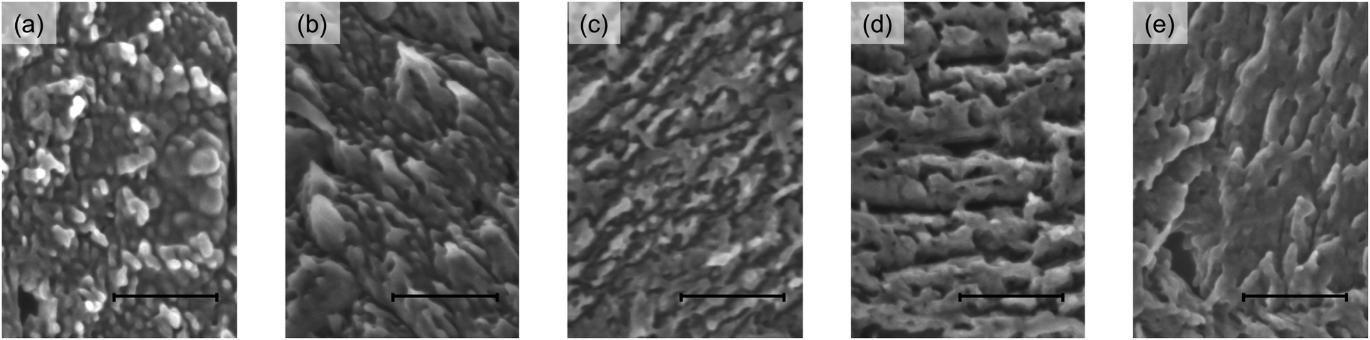 | ||
| Fig. 5 SEM images of Structure II surfaces corresponding to devices with different amounts of BP–C60: (a) 0 wt%, (b) 3 wt%, (c) 5 wt%, (d) 7 wt%, and (e) 10 wt%. Scale bars correspond to 200 nm. | ||
The nanoscale features observed by SEM suggested the size of the p–n interface was best for Structure II (5 wt%), thus enhancing charge separation and charge transport to the appropriate electrodes. The p–i–n (5 wt%) device exhibited the best performance, namely, an improved JSC value at 6.81 mA cm−2 and the highest FF value at 0.61. This result can be attributed to its i-layer structure, wherein there exists a balance between the charge-carrier generation and transport.
Conclusions
In this work, we demonstrated that the structure of the i-layer of solution-processable p–i–n devices based on BP:PC61BM can be modified readily by adding a small amount of BP–C60 to improve the device performance. The p–i–n devices containing BP–C60 in the i-layer showed significantly improved performance (PCE = 2.38%) as compared to that of a device without BP–C60 (PCE = 1.58%) and even surpassed the record performance of the BP:PC61BM-based p–i–n device (PCE = 2.0%) reported by Matsuo et al.54 The presence of BP–C60 in the i-layer affects the layer morphology, phase separation, and crystallinity. AFM and fluorescence microspectroscopy measurements suggested that, when BP–C60 is introduced into the i-layer, the domain size is reduced, leading to the formation of a larger p–n interface for charge-carrier generation as well as smoother i- and n-layers, which result in better semiconducting behavior. In addition, the interfacial BP network, which was investigated by SEM, is also modified by the presence of BP–C60. However, the presence of excessive BP–C60 can be lead to the deterioration of the p–n interface and limit carrier transport in the active layer. On the other hand, despite the morphological changes induced with the addition of BP–C60, the crystal orientation does not change, but the crystallinity of both BP and PC61BM decreases gradually. Thus, it is essential to add BP–C60 in the appropriate amount in order to ensure that it has the desired positive effect as a morphological additive.For the high charge carrier mobility of small molecular organic semiconductors, good crystallinity with high transfer integral is critical. The good crystallinity also brings the stability of the organic electronic devices. On the other hand, the good crystallinity often disturbs the miscibility of donor and acceptor materials, that is necessary for effective charge generation in OPVs. BP is one of the superior and promising p-type organic semiconductors with high crystallinity and several groups reported the improvement of the miscibility of BP and acceptor materials by the derivatization of BP and PC61BM, as described in Introduction. However, it is important to improve the PCE performance without changing the chemical structure of BP and PC61BM, a standard combination, to give the general and universal information about the additive effect of connected donor–acceptor molecule to i-layer in small molecular OPVs.
The fact that fullerene-linked materials allow for the morphological control of solution-processed small molecules in thin films suggests that they have enormous potential for fabricating suitable heterojunctions. Although this study focused on the performance of p–i–n devices based on the BP:PC61BM system, the result that the addition of even a small amount of a fullerene-linked molecule can enhance the photovoltaic performance suggests a new opportunity for improving the performance of small-molecule-based OSCs.
Experimental
Materials
CP and CP–C60 were prepared according to the reported procedures.56,67Thin film preparation and device fabrication for OSC
Patterned-ITO/glass substrates (20 mm × 25.0 mm, <15 Ω per square) were washed with running water and were ultrasonically cleaned in detergent, pure-water and isopropanol for 10 min each. After the substrates were dried, (3,4-ethylenedioxythiophene):poly(4-styrenesulfonate) (PEDOT:PSS, Clevios P VP AI4083) was spin-coated (3000 rpm, 30 s) under air followed by a thermal annealing treatment at 130 °C for 10 min. The substrates were transferred to a nitrogen-filled glove box (<10.0 ppm O2 and H2O). The p-layer was prepared by spin coating (1500 rpm, 30 s) of a CP-solution (7 mg mL−1 in chloroform) followed by heating (200 °C, 10 min) to effect the in situ conversion of CP to BP. The i-layers were deposited by spin coating (1500 rpm, 30 s) a CP:PC61BM (1:1.5 wt/wt)-solution (10 mg mL−1, chloroform) containing 0–10 wt% of CP–C60 followed by heating (180 °C, 20 min) to effect the in situ conversion to BP:PC61BM containing BP–C60. The n-layer was prepared by spin coating (1500 rpm, 30 s) of PC61BM-solution (7 mg mL−1 in chloroform), which was then annealed (195 °C, 10 min). After preparation of the active layers, the buffer layer (Ca, 5 nm) and counter electrode (Al, 50 nm) were vapor deposited at a high vacuum (<5.0 × 10⁻¹ Pa) through a shadow mask with a defined active area of 4 mm2. Finally, the fabricated organic solar cell was encapsulated with backing glasses using a UV-curable resin under nitrogen atmosphere.
OSC performances
Current density–voltage (J–V) curves were measured using a Keithley 2611B SYSTEM Source Mater unit under AM1.5G illumination at an intensity of 100 mW cm−2 using a solar simulator (Bunko-keiki, CEP-2000RP). The external quantum efficiency (EQE) spectra were obtained under illumination of monochromatic light using the same system.SCLC measurement
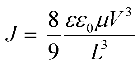
The SCLC device structures for hole-only and electron-only measurements were [ITO/MoO3/active layer/MoO3/Al] and [ITO/ZnO/active layer/LiF/Al], respectively. For hole only device, MoO3 (15 nm) was vapor deposited on the cleaned ITO/glass substrate at high vacuum (<5.0 × 10⁻⁴ Pa). For electron only device, ZnO film (28 nm) was prepared by sol–gel method using the ZnO precursor solution.29 The ZnO precursor solution was spin coated (5000 rpm, 30 s) on the cleaned ITO/glass substrate followed by heating (300 °C, 1 h) under air condition to obtain the ZnO film. Then, substrates were transferred to a N2-filled glove box (<10.0 ppm O2 and H2O). Each active layer was prepared by spin coating of CP:PC61BM solution with and without CP–C60 in chloroform (14 mg mL−1) at 800 rpm for 30 s on ITO/MoO3 (15 nm) or ITO/ZnO (28 nm), respectively. After spin coating, these films were heated in the same condition for the OPV device fabrication to convert to BP:PC61BM solution with and without BP–C60 in the nitrogen-filled glove box. After preparation of the organic layers, MoO3 (15 nm)/Al (50 nm) or LiF (1 nm)/Al (50 nm) were vapor deposited at high vacuum (<5.0 × 10⁻⁴ Pa). Current–voltage (J–V) curves of fabricated SCLC devices were measured by Keithley 2400 source-measure unit in air. To estimate the charge mobility, curve fitting was performed according to the formula as follows,where ε is the dielectric constant, ε0 is the permittivity of space, μ is the charge mobility. V is the applied voltage, and L is the active layer thickness. The dielectric constant ε is assumed to be 3, which is atypical value for organic semiconductors.
Film thickness
Active layer thickness was measured by a Surface Profiler ET200 (Kosaka Laboratory Ltd). The value was obtained as an average of 10 measurement points.Atomic force microscopy (AFM)
The surface morphology of organic films was observed by an SPA400, SPI3800N AFM (Seiko instruments Inc.) in tapping mode using silicon probes with a resonant frequency of ∼138 kHz and a force constant of 16 N m−1.Scanning electron microscopy (SEM)
The surface texture of organic films was observed by an Ultra High-Resolution Scanning Electron Microscope SU9000 (Hitachi, Ltd.) with accelerating voltage of 1.0 kV. The sample film surface was not deposited with conductive materials for prevention of static charge. The thin-film samples for these measurements were prepared on PEDOT:PSS-coated ITO/glass substrates in the same manner as in the device fabrication described above.Scanning transmission electron microscopy (STEM)
The cross-sectional structure of organic films was observed by a HD-2700 (Hitachi, Ltd.) which combines an Energy Dispersive X-ray (EDX) spectroscopy Octane T Ultra W 100mm2SDD (AMETEK). For this measurement, Focused Ion Beam System FB2200 (Hitachi, Ltd.) has been used for site-specific preparation of cross sectional samples suitable for STEM analysis using the micro sampling technique.72Fluorescence microspectroscopy
The fluorescence from the Structure I was collected by an objective lens (60×, N.A.:0.7, LUCPlanFLN, Olympus) and passed through a confocal pinhole (100 μm) and suitable filters. To detect the fluorescence of the BP, a 405 nm laser was used as an excitation source, and a long-pass filter (LP02-442RU, Semrock) and a short-pass filter (FF01-650/SP, Semrock) were used to cut the excitation laser beam and fluorescence from PC61BM, respectively. The detected fluorescence was split into two paths by a 50/50 beam splitter, and the two paths were detected using a spectrometer (SpectraPro2358, Acton Research Corporation) with a cooled CCD camera (PIXIS400B, Princeton Instruments) and an avalanche single-photon counting module (APD: SPCM-AQR-14, PerkinElmer). The signal from the APD was connected to a time-correlated single-photon counting board (SPC-630, Becker & Hickl) for the fluorescence images.Two-dimensional grazing-incident wide-angle X-ray diffraction (2D-GIWAXD) measurements
D-GIWAXD measurements were performed in a HUBER multiaxis diffractometer installed in beamline BL-19B2 at SPring-8 (Hyogo, Japan). The X-ray beam was monochromatized by a double-crystal Si (111) monochromator, and the X-ray energy was 12.398 keV. Scattered X-rays from samples were detected by an X-ray photon counting pixel detector (PILATUS 300 K). The X-ray-beam incidence angle was set to 0.12°, and the sample-to-detector distance was about 174 mm. The thin-film samples for the GIWAXD measurements were prepared on ITO-coated glass substrates in the same manner as in the device fabrication described above. All of sample substrates were kept a certain size (10 mm × 10 mm) to receive a similar effect of the footprint.Conflicts of interest
There are no conflicts to declare.Acknowledgements
This work was partly supported by CREST, JST, Grants-in-Aid for Scientific Research (No. JP26105004, JP16H02286, JP16K17949 and JP17H03042) and the Grant-in-Aid for JSPS Research Fellow program for Young Scientists. We thank The Nippon Synthetic Chemical Industry Co., Ltd. (Osaka, Japan) for providing ethyl isocyanoacetate, the starting material for the synthesis of CP. We also thank Mr K. Miyake of NAIST for assistance with the SEM and STEM measurements. The synchrotron experiments were performed at beamline BL-19B2 of the Spring-8 facility with the approval of the Japan Synchrotron Radiation Research Institute (JASRI) (Proposal No. 2017A1779).Notes and references
- M. Kaltenbrunner, M. S. White, E. D. Głowacki, T. Sekitani, T. Someya, N. S. Sariciftci and S. Bauer, Nat. Commun., 2012, 3, 770 CrossRef PubMed.
- F. C. Krebs, Org. Electron., 2009, 10, 761–768 CrossRef CAS.
- D. Angmo, S. A. Gevorgyan, T. T. Larsen-Olsen, R. R. Søndergaard, M. Hösel, M. Jørgensen, R. Gupta, G. U. Kulkarni and F. C. Krebs, Org. Electron., 2013, 14, 984–994 CrossRef CAS.
- G. A. dos Reis Benatto, B. Roth, M. Corazza, R. R. Søndergaard, S. A. Gevorgyan, M. Jørgensen and F. C. Krebs, Nanoscale, 2016, 8, 318–326 RSC.
- M. Finn, C. J. Martens, A. V. Zaretski, B. Roth, R. R. Søndergaard, F. C. Krebs and D. J. Lipomi, Sol. Energy Mater. Sol. Cells, 2018, 174, 7–15 CrossRef CAS.
- H. Benten, D. Mori, H. Ohkita and S. Ito, J. Mater. Chem. A, 2016, 4, 5340–5365 RSC.
- S. Li, W. Liu, C.-Z. Li, M. Shi and H. Chen, Small, 2017, 1701120 CrossRef PubMed.
- Y. Lin and X. Zhan, Mater. Horiz., 2014, 1, 470 RSC.
- Y. Lin and X. Zhan, Adv. Energy Mater., 2015, 5, 150163 Search PubMed.
- I. Etxebarria, J. Ajuria and R. Pacios, Org. Electron., 2015, 19, 34–60 CrossRef CAS.
- W. Chen, X. Yang, G. Long, X. Wan, Y. Chen and Q. Zhang, J. Mater. Chem. C, 2015, 3, 4698–4705 RSC.
- H. Sun, X. Song, J. Xie, P. Sun, P. Gu, C. Liu, F. Chen, Q. Zhang, Z.-K. Chen and W. Huang, ACS Appl. Mater. Interfaces, 2017, 9, 29924–29931 CrossRef CAS PubMed.
- W. Chen and Q. Zhang, J. Mater. Chem. C, 2017, 5, 1275–1302 RSC.
- Z. He, C. Zhong, S. Su, M. Xu, H. Wu and Y. Cao, Nat. Photonics, 2012, 6, 591–595 CrossRef.
- J. You, L. Dou, K. Yoshimura, T. Kato, K. Ohya, T. Moriarty, K. Emery, C. C. Chen, J. Gao, G. Li and Y. A. Yang, Nat. Commun., 2013, 4, 1410–1446 CrossRef PubMed.
- A. J. Heeger, Adv. Mater., 2014, 26, 10–28 CrossRef CAS PubMed.
- M. C. Scharber and N. S. Sariciftci, Prog. Polym. Sci., 2013, 38, 1929–1940 CrossRef CAS PubMed.
- Z. He, B. Xiao, F. Liu, H. Wu, Y. Yang, S. Xiao, C. Wang, T. P. Russell and Y. Cao, Nat. Photonics, 2015, 9, 174–179 CrossRef CAS.
- J. Huang, J. H. Carpenter, C. Z. Li, J. S. Yu, H. Ade and A. K. Y. Jen, Adv. Mater., 2016, 28, 967–974 CrossRef CAS PubMed.
- J. Huang, H. Wang, K. Yan, X. Zhang, H. Chen, C.-Z. Li and J. Yu, Adv. Mater., 2017, 29, 1606729 CrossRef PubMed.
- J. Huang, X. Zhang, D. Zheng, K. Yan, C.-Z. Li and J. Yu, Sol. RRL, 2017, 1, 1600008 CrossRef.
- T. Kumari, S. M. Lee, S.-H. Kang, S. Chen and C. Yang, Energy Environ. Sci., 2017, 10, 258–265 RSC.
- S. Li, L. Ye, W. Zhao, S. Zhang, S. Mukherjee, H. Ade and J. Hou, Adv. Mater., 2016, 28, 9423–9429 CrossRef CAS PubMed.
- Y. Liu, J. Zhao, Z. Li, C. Mu, W. Ma, H. Hu, K. Jiang, H. Lin, H. Ade and H. Yan, Nat. Commun., 2014, 5, 5293 CrossRef CAS PubMed.
- F. Zhao, S. Dai, Y. Wu, Q. Zhang, J. Wang, L. Jiang, Q. Ling, Z. Wei, W. Ma, W. You, C. Wang and X. Zhan, Adv. Mater., 2017, 29, 1700144 CrossRef PubMed.
- M. A. Ruderer, S. Guo, R. Meier, H. Y. Chiang, V. Körstgens, J. Wiedersich, J. Perlich, S. V. Roth and P. Müller-Buschbaum, Adv. Funct. Mater., 2011, 21, 3382–3391 CrossRef CAS.
- H. C. Liao, C. C. Ho, C. Y. Chang, M. H. Jao, S. B. Darling and W. F. Su, Mater. Today, 2013, 16, 326–336 CrossRef CAS.
- J. Peet, J. Y. Kim, N. E. Coates, W. L. Ma, D. Moses, A. J. Heeger and G. C. Bazan, Nat. Mater., 2007, 6, 497–500 CrossRef CAS PubMed.
- M. Suzuki, Y. Yamaguchi, K. Takahashi, K. Takahira, T. Koganezawa, S. Masuo, K. Nakayama and H. Yamada, ACS Appl. Mater. Interfaces, 2016, 8, 8644–8651 CrossRef CAS PubMed.
- G. J. Zhao, Y. J. He and Y. Li, Adv. Mater., 2010, 22, 4355–4358 CrossRef CAS PubMed.
- X. Yang and A. Uddin, Renewable Sustainable Energy Rev., 2014, 30, 324–336 CrossRef CAS.
- O. K. Kwon, M. A. Uddin, J. H. Park, S. K. Park, T. L. Nguyen, H. Y. Woo and S. Y. Park, Adv. Mater., 2016, 28, 910–916 CrossRef CAS PubMed.
- Q. Zhang, B. Kan, F. Liu, G. Long, X. Wan, X. Chen, Y. Zuo, W. Ni, H. Zhang, M. Li, Z. Hu, F. Huang, Y. Cao, Z. Liang, M. Zhang, T. P. Russell and Y. Chen, Nat. Photonics, 2014, 9, 35–41 CrossRef.
- J. L. Wang, K. K. Liu, J. Yan, Z. Wu, F. Liu, F. Xiao, Z. F. Chang, W. H. Bin, Y. Cao and T. P. Russell, J. Am. Chem. Soc., 2016, 138, 7687–7697 CrossRef CAS PubMed.
- G. Wei, S. Wang, K. Sun, M. E. Thompson and S. R. Forrest, Adv. Energy Mater., 2011, 1, 184–187 CrossRef CAS.
- K. Wang, M. Azouz, M. Babics, F. Cruciani, T. Marszalek, Q. Saleem, W. Pisula and P. M. Beaujuge, Chem. Mater., 2016, 28, 5415–5425 CrossRef CAS.
- J.-L. Wang, F. Xiao, J. Yan, Z. Wu, K.-K. Liu, Z.-F. Chang, R.-B. Zhang, H. Chen, H.-B. Wu and Y. Cao, Adv. Funct. Mater., 2016, 26, 1803–1812 CrossRef CAS.
- J. L. Wang, Z. Wu, J.-S. Miao, K.-K. Liu, Z.-F. Chang, R.-B. Zhang, H.-B. Wu and Y. Cao, Chem. Mater., 2015, 27, 4338–4348 CrossRef CAS.
- S. Miller, G. Fanchini, Y.-Y. Lin, C. Li, C.-W. Chen, W.-F. Su and M. Chhowalla, J. Mater. Chem., 2008, 18, 306–312 RSC.
- J. Miao, H. Chen, F. Liu, B. Zhao, L. Hu, Z. He and H. Wu, Appl. Phys. Lett., 2015, 106, 183302 CrossRef.
- S. Grob, A. N. Bartynski, A. Opitz, M. Gruber, F. Grassl, E. Meister, T. Linderl, U. Hörmann, C. Lorch, E. Moons, F. Schreiber, M. E. Thompson and W. Brütting, J. Mater. Chem. A, 2015, 3, 15700–15709 RSC.
- K. Gao, W. Deng, L. Xiao, Q. Hu, Y. Kan, X. Chen, C. Wang, F. Huang, J. Peng, H. Wu, X. Peng, Y. Cao, T. P. Russell and F. Liu, Nano Energy, 2016, 30, 639–648 CrossRef CAS.
- T. Motoyama, S. Sugii, S. Ikeda, Y. Yamaguchi, H. Yamada and K. Nakayama, Jpn. J. Appl. Phys., 2014, 53, 01AB02 CrossRef.
- H. Yamada, C. Ohashi, T. Aotake, S. Katsuta, Y. Honsho, H. Kawano, T. Okujima, H. Uno, N. Ono, S. Seki and K. Nakayama, Chem. Commun., 2012, 48, 11136–11138 RSC.
- H. Yamada, Y. Yamaguchi, R. Katoh, T. Motoyama, T. Aotake, D. Kuzuhara, M. Suzuki, T. Okujima, H. Uno, N. Aratani and K. Nakayama, Chem. Commun., 2013, 49, 11638–11640 RSC.
- T. Motoyama, T. Kiyota, H. Yamada and K. Nakayama, Sol. Energy Mater. Sol. Cells, 2013, 114, 156–160 CrossRef CAS.
- N. Noguchi, S. Junwei, H. Asatani and M. Matsuoka, Cryst. Growth Des., 2010, 10, 1848–1853 CrossRef CAS.
- A. S. Dhoot, S. Aramaki, D. Moses and A. J. Heeger, Adv. Mater., 2007, 19, 2914–2918 CrossRef CAS.
- P. B. Shea, H. Yamada, N. Ono and J. Kanicki, Thin Solid Films, 2012, 520, 4031–4035 CrossRef CAS.
- H. Saeki, M. Misaki, D. Kuzuhara, H. Yamada and Y. Ueda, Jpn. J. Appl. Phys., 2013, 52, 111601 CrossRef.
- T. Umeyama, K. Hirose, K. Noda, K. Matsushige, T. Shishido, H. Saarenpää, N. V. Tkachenko, H. Lemmetyinen, N. Ono and H. Imahori, J. Phys. Chem. C, 2012, 116, 17414–17423 CrossRef CAS.
- A. Hirao, T. Akiyama, T. Okujima, H. Yamada, H. Uno, Y. Sakai, S. Aramaki and N. Ono, Chem. Commun., 2008, 39, 4714–4716 RSC.
- Y. Yamaguchi, M. Suzuki, T. Motoyama, S. Sugii, C. Katagiri, K. Takahira, S. Ikeda, H. Yamada and K. Nakayama, Sci. Rep., 2014, 4, 7151 CrossRef CAS PubMed.
- Y. Matsuo, Y. Sato, T. Niinomi, I. Soga, H. Tanaka and E. Nakamura, J. Am. Chem. Soc., 2009, 131, 16048–16050 CrossRef CAS PubMed.
- M. Guide, X. D. Dang and T. Q. Nguyen, Adv. Mater., 2011, 23, 2313–2319 CrossRef CAS PubMed.
- S. Ito, T. Murashima, N. Ono and H. Uno, Chem. Commun., 1998, 16, 1661–1662 RSC.
- M. Suzuki, Y. Yamaguchi, K. Uchinaga, K. Takahira, C. Quinton, S. Yamamoto, N. Nagami, M. Furukawa, K. Nakayama and H. Yamada, Chem. Sci., 2018, 9, 6614–6621 RSC.
- K. Sivula, Z. T. Ball, N. Watanabe and J. M. J. Fréchet, Adv. Mater., 2006, 18, 206–210 CrossRef CAS.
- J. U. Lee, J. W. Jung, T. Emrick, T. P. Russell and W. H. Jo, Nanotechnology, 2010, 21, 105201 CrossRef PubMed.
- J. U. Lee, A. Cirpan, T. Emrick, T. P. Russell and W. H. Jo, J. Mater. Chem., 2009, 19, 1483–1489 RSC.
- C. Yang, J. K. Lee, A. J. Heeger and F. Wudl, J. Mater. Chem., 2009, 19, 5416 RSC.
- J. U. Lee, J. W. Jung, T. Emrick, T. P. Russell and W. H. Jo, J. Mater. Chem., 2010, 20, 3287 RSC.
- J. B. Kim, K. Allen, S. J. Oh, S. Lee, M. F. Toney, Y. S. Kim, C. R. Kagan, C. Nuckolls and Y. L. Loo, Chem. Mater., 2010, 22, 5762–5773 CrossRef CAS.
- Y. C. Lai, T. Higashihara, J. C. Hsu, M. Ueda and W. C. Chen, Sol. Energy Mater. Sol. Cells, 2012, 97, 164–170 CrossRef CAS.
- L. Chen, K. Yao and Y. Chen, J. Mater. Chem., 2012, 22, 18768 RSC.
- Y. Tamura, H. Saeki, J. Hashizume, Y. Okazaki, D. Kuzuhara, M. Suzuki, N. Aratani and H. Yamada, Chem. Commun., 2014, 50, 10379–10381 RSC.
- Y. Tamura, D. Kuzuhara, M. Suzuki, H. Hayashi, N. Aratani and H. Yamada, J. Mater. Chem. A, 2016, 4, 15333–15342 RSC.
- O. V. Mikhnenko, P. W. M. Blom and T.-Q. Nguyen, Energy Environ. Sci., 2015, 8, 1867–1888 RSC.
- S. Aramaki and J. Mizuguchi, Acta Crystallogr., Sect. E: Struct. Rep. Online, 2003, 59, o1556–o1558 CrossRef CAS.
- C. D. Liman, S. Choi, D. W. Breiby, J. E. Cochran, M. F. Toney, E. J. Kramer and M. L. Chabinyc, J. Phys. Chem. B, 2013, 117, 14557–14567 CrossRef CAS PubMed.
- E. D. Gomez, K. P. Barteau, H. Wang, M. F. Toney and Y.-L. Loo, Chem. Commun., 2011, 47, 436–438 RSC.
- R. J. Young and M. V. Moore, Dual-Beam (FIB-SEM) Systems Techniques and Automated Applications, 2005 Search PubMed.
Footnote |
| † Electronic supplementary information (ESI) available: Out-of-plane XRD data, UV-vis absorption spectra of p–i–n devices, 1D line cut of 2D-GIWAXD patterns with line fitting, figures of BP crystal with (101) and (200) planes, and additional AFM, SEM, and STEM images. See DOI: 10.1039/c8ra07398h |
| This journal is © The Royal Society of Chemistry 2018 |