
 Open Access Article
 This Open Access Article is licensed under a Creative Commons Attribution-Non Commercial 3.0 Unported Licence
Nanowire network-based photodetectors with imaging performance for omnidirectional photodetecting through a wire-shaped structure†
Shalong Wang,
Yousheng Zou*,
Qingsong Shan,
Jie Xue,
Yuhui Dong,
Yu Gu and
Jizhong Song *
*
Institute of Optoelectronics & Nanomaterials, MIIT Key Laboratory of Advanced Display Materials and Devices, School of Materials Science and Engineering, Nanjing University of Science & Technology, Nanjing 210094, China. E-mail: songjizhong@njust.edu.cn; yshzou75@njust.edu.cn
First published on 1st October 2018
Abstract
Wearable photodetectors (PDs) have attracted extensive attention from both scientific and industrial areas due to intrinsic detection abilities as well as promising applications in flexible, intelligent, and portable fields. However, most of the existing PDs have rigid planar or bulky structures which cannot fully meet the demands of these unique occasions. Here, we present a highly flexible, omnidirectional PD based on ZnO nanowire (NW) networks. ZnO NW network-based PDs exhibit the imageable level performance with an on/off ratio of about 104. Importantly, a ZnO NW network can be assembled onto wire-shaped substrates to construct omnidirectional PDs. As a result, the wire-shaped PDs have excellent flexibility, a large light on/off ratio larger than 103, and 360° no blind angle detecting. Besides, they exhibit extraordinary stability against bending and irradiation. These results demonstrate a novel strategy for building wire-shaped optoelectronic devices through a NW network structure, which is highly promising for future smart and wearable applications.
Introduction
Wearable electronics and optoelectronics, which are also known as smart textiles or integration of electronic devices with textiles, have attracted extensive attention from both scientific and industrial areas.1–5 Among various smart devices, photodetectors (PDs) have a wide range of applications in missile detection, biological sensing, flame sensing, optical communications, astronomical studies, chemical analysis, medical diagnostics, digital imaging, environmental monitoring, remote control, and optoelectronic circuits, which have been extensively studied.6–14 However, most existing PDs have planar or bulky structures, which cannot fully meet the urgent demands of portable, flexible, and wearable applications.15,16 Compared with planar structures, wire-shaped or/and fiber-shaped photodetecting components, easily woven into textiles or other structures, have been proven to have a huge potential due to their high flexibility, knittability, small size and light weight.17–19However, so far, the performances of wire-shaped PDs are still lower than their corresponding planar devices, because the existing wire-shaped PDs are mostly core–shell structures with an electrode inside the device and another electrode outside. Such a vertical structure will contribute to a high level of current in dark conditions, which more often than not cause low performance of the low on/off ratio. For example, Ko17 et al. fabricated wire-shaped ultraviolet PDs based on a nanostructured zinc oxide (ZnO)/nickel oxide (NiO) coaxial p–n heterojunction with a light on/off ratio of about 10. Chen20 et al. reported a UV wire-PD with ZnO nanowires (NWs) grown on an oxidized Ni wire, and the light on/off ratio was about 4. A self-powered fiber-shaped wearable omnidirectional ultraviolet (UV) PD with a light on/off ratio of 2 under zero bias was constructed by Dong and her co-authors.6 Therefore, it is desirable to design an all-purpose structure with excellent photodetecting performances for future wearable devices.
Various NW networks have been considered as a class of promising optoelectronic materials for flexible, stretchable, and wearable devices, owing to their superior elasticity for bending, stretching, twisting, and deformation into complex, non-planar shapes.21–24 In general, the strain applied by a mechanical stretching stress is accommodated by rotations and distortions of the NW network.25–27 Thus, unconventional nanostructures, which are generated by spatial displacement between NWs with a high aspect ratio, can maintain their continuous network structures, which act as an electrical charge path, guaranteeing excellent carrier transporting properties under various deformations. Thus, there is a high potential to develop wire-shaped PDs based on a NWs network for wearable devices.
Here, we present omnidirectional PDs based on a ZnO NW network, which is promising for future wearable and smart optoelectronic devices. First, high quality ZnO NWs with large aspect ratios of >100 are readily dispersed in alcoholic solvents, e.g., isopropanol, serving as ink. The ink can be used to process highly uniform NWs network films for various optoelectronic devices. NW network-based PDs exhibit an imageable level performance with an on/off ratio of about 104. Importantly, a ZnO NW network can be transferred onto wire-shaped substrates to construct omnidirectional PDs. As a result, the wire-shaped PDs have excellent flexibility (>500 cycles), large light on/off ratio of 103, and 360° no blind angle detecting. These results demonstrate a novel strategy to build the wire-shaped optoelectronic devices suitable for future smart and wearable applications.
Experimental section
1 Synthetic procedures
The as-obtained ZnO NWs were put in isopropanol and sonicated for 60 s to prepare a nanowire dispersion (typically with a concentration of 0.1 mg mL−1). Commercially available CNTs wire (diameter of 20–30 μm and density of 0.3–0.5 g cm−3, from SCNC Company) was used as the electrode.KEVLAR wire with diameter of 1 mm was dipped in PDMS gel and pre-cured at 60 °C for 1 h. The PDMS (Sylgard 184, Dow Corning) gel was prepared from a mixture of a base and a curer (weight ratio 10![[thin space (1/6-em)]](https://www.rsc.org/images/entities/char_2009.gif) :1). The KEVLAR wire was rotated on a PVDF filter membrane with the ZnO NWs. The sample was further twisted with CNT fiber wire to construct the PDs and then the devices were packaged with a thin layer of PDMS for testing.
:1). The KEVLAR wire was rotated on a PVDF filter membrane with the ZnO NWs. The sample was further twisted with CNT fiber wire to construct the PDs and then the devices were packaged with a thin layer of PDMS for testing.
2 Materials characterization
The morphologies of the NWs and devices were characterized using field-emission SEM (FE-SEM) (JSM 7600F). TEM images of ZnO NWs were measured with FEI Tecnai G20 on a Cu grid. The photoresponse behaviours of the devices were characterized using a Keithley 6487 analyzer with a portable UV LED as the light source (365 nm). Responsivities of the PDs were measured by a detector test system from ZOLIX INSTRUMENTS CO. Ltd with a Si PD as reference. The device was fixed on a home-made stretching stage to apply strain for flexible measurements. All measurements were performed at room temperature in ambient conditions.Results and discussion
ZnO NW (purchased from Hebei ShaoJing New Material Technology Co., Ltd.) can be readily dispersed in alcoholic solvents, e.g., isopropanol, serving as ink (Fig. 1a). The NW ink is compatible with several well-documented solution-processed thin-film deposition techniques, such as spray coating, scrape coating, and filtration. The ZnO NWs possess an average diameter of ∼35 nm (Fig. 1b) and an average length of more than 20 μm (Fig. S1†). Such great length and large aspect ratio (>500) will favor their conductivity due to the resulting long and smooth transport channels for electrons. The microstructure of ZnO NWs was further confirmed by transmission electron microscopy (TEM) as shown in Fig. 1c–e. Fig. 1c clearly shows that the 35 nm NW has a very smooth and clean surface without any coating layer. The high resolution TEM (HRTEM) image in Fig. 1d exhibits lattice fringes of 0.52 nm, corresponding to the (001) plane normal to the growth direction, which is consistent with that of wurtzite ZnO crystal structure.28,29 Besides, the HRTEM image reveals a perfect lattice without any visible defects, which reflects the high crystallinity of ZnO NWs. The selected area electron diffraction (SAED) pattern shown in Fig. 1e also confirms that ZnO NWs have a good crystallinity, exhibiting a set of reflections corresponding to the [001] crystallographic direction of ZnO and being consistent with HRTEM. The high crystallinity ZnO NWs are very favorable for carrier transporting, which are highly promising in various optoelectronic devices.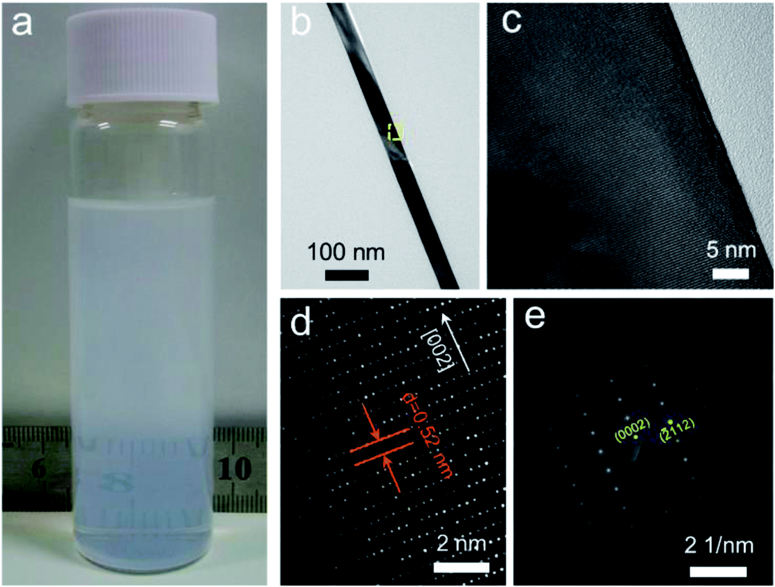 | ||
| Fig. 1 (a) Photograph of ZnO NW inks re-dispersed in isopropanol. (b) TEM image of a ZnO NW with diameter of about 35 nm. (c) Magnified TEM image of the surface of a ZnO NW. (d) High-resolution TEM image and (e) SAED pattern of ZnO NWs. | ||
As shown in Fig. 1a, upon sonication for 1 min, the ZnO NWs formed a dispersion in isopropanol. The NW inks were filtered with a polyvinylidene fluoride (PVDF) membrane to form a thin and uniform film, which then could be easily transferred onto various substrates. Fig. 2a shows the large-area ZnO NW network transferred onto glass substrates characterized by SEM images. The ZnO NWs lay on the substrate due to their unique 1D geometries, and can be assembled into dense, crack-free, and smooth films observed by the photograph (inset in Fig. 2a). The high magnification SEM image shown in Fig. 2b demonstrates that ZnO NWs are intertwined together to form a perfect network structure. As described in the introduction, such network structure, which is very favorable for adapting to the deformations under applied stress, could maintain high flexibility. Accordingly, the flexible ZnO NWs network transferred onto flexible polyethylene terephthalate (PET) and stretchable polydimethylsiloxane (PDMS) substrates are shown in Fig. 2c and d. Especially, after bending and recovering for about 500 times the NWs on the PDMS substrates still retained their integrity. This is ascribed to the NWs being partially embedded in PDMS polymer, which anchored the NW network and further preserved the integrity of junctions among the NWs.
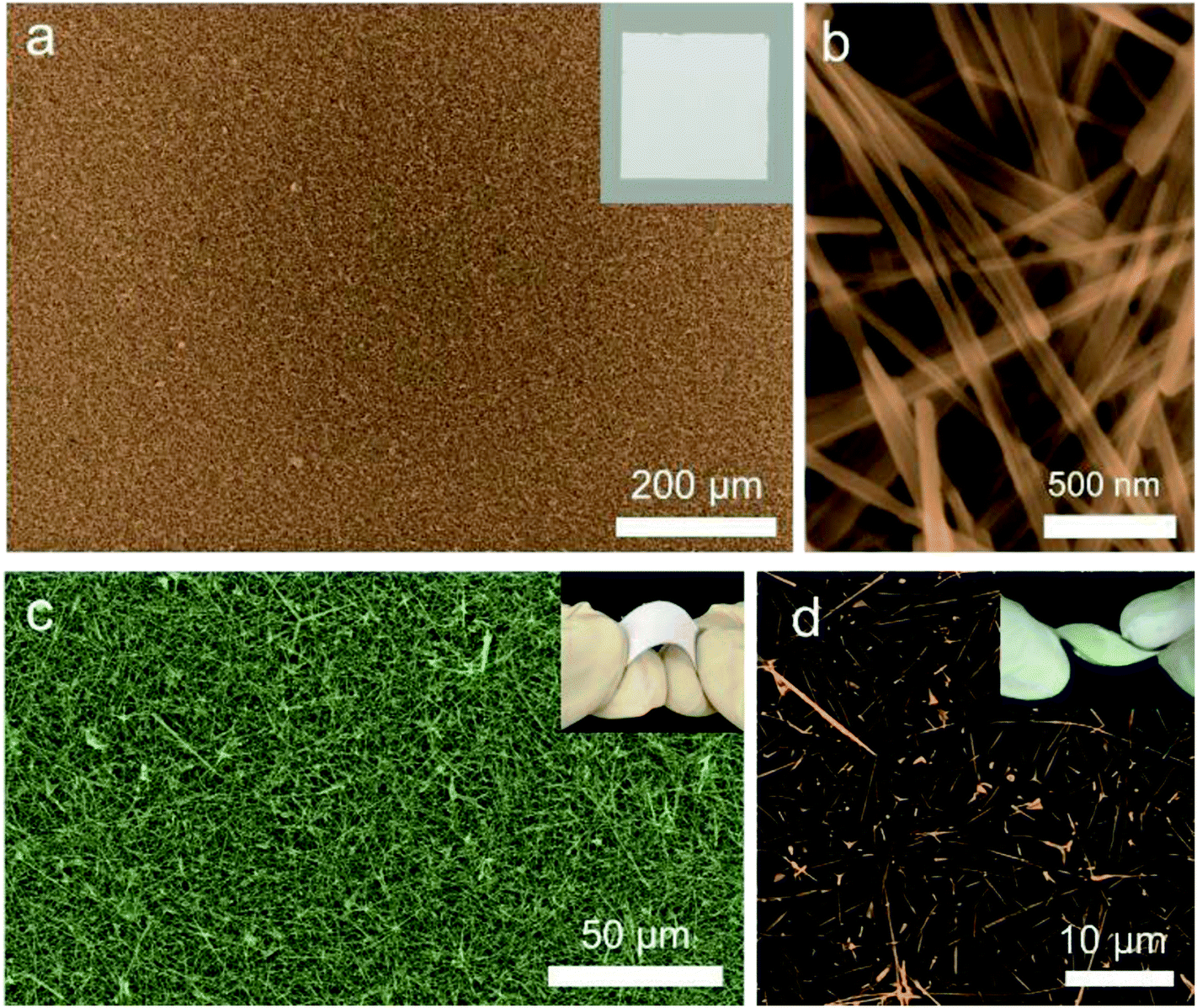 | ||
| Fig. 2 ZnO NW networks on various substrates. (a) Large-area SEM images of the ZnO NW network film transferred on a glass substrates, inset: photograph of ZnO NW network film on a glass substrate. (b) High magnification SEM image of ZnO NWs on a glass substrate. SEM images of the ZnO NW network film transferred onto (c) PET and (d) PDMS substrates, insets: the corresponding photograph of ZnO NW network film on PET and PDMS substrates, respectively. | ||
The photoelectric response characteristics of a ZnO NW network are presented in Fig. 3. The device configuration of a ZnO NW network PD is schematically demonstrated in Fig. S2;† Au interdigital electrodes were deposited on ZnO network substrates. Fig. 3a and b show the I–V and I–V logarithm characteristics of a ZnO NW network PD in the dark and under 365 nm (0.35 mW cm−2) illumination, respectively. The linear I–V relationship with forward and reverse bias measured in the dark clearly shows an approximate ohmic contact between the ZnO NW network and electrodes.30,31 The NW network exhibits high photoresponse. For example, the dark current and photocurrent are 7.73 nA, and 30 μA at 5 V applied bias, respectively whereby the resulting on/off current ratio was calculated to be 3.9 × 10³ at 5 V.
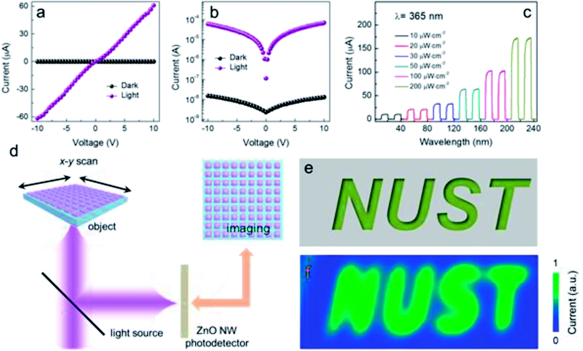 | ||
| Fig. 3 Imageable photoelectric response characteristics of ZnO NW network. (a) I–V and (b) I–V logarithm characteristics of ZnO NW PD in the dark and under 365 nm (0.35 mW cm−2) illumination. (c) I–t curves at 5 V of ZnO NW PD under 365 nm with different light irradiation intensity. (d) Schematic of the PD imaging setup. (e) Object and (f) image acquired from the ZnO nanowire PD at λ of 365 nm. | ||
To illustrate the light-switching characteristic, the photocurrent–time response measured in the dark and under illumination was controlled by a light shutter. As shown in Fig. S3,† when the UV light was turned on, the photocurrent sharply increased under the applied bias voltage. Meanwhile, the device immediately decayed to a dark current as soon as the UV light was turned off. The device exhibited stable and reproducible responses to on–off cycles. The current–time (I–t) curves at 2 V bias under 365 nm laser (1 mW cm−2) with different light irradiation intensity are presented in Fig. 3c. As shown in this picture, under illumination the device produced a photocurrent which steadily increased with increasing light power from 10 μW cm−2 to 200 μW cm−2. Especially, the current measured at 2 V reached a maximum value of 64 μA with a light intensity of 50 μW cm−2, which is about 3 orders of magnitude compared with that under dark conditions.
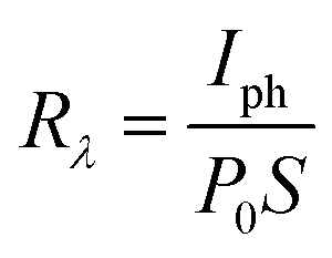
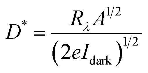
Furthermore, the spectral responsivity of the device considered as a function of excitation wavelengths was measured. The responsivity Rλ was calculated according to the following equation:32
 | (1) |
The detectivity (D*), demonstrated the ability of the photodetector for detecting a weak signal, also a critical parameter, which is calculated by the following equation:
 | (2) |
To further demonstrate the high photoresponse properties, a distinct imaging picture with letters of NUST (Nanjing University of Science and Technology) is demonstrated in Fig. 3d–f. The photocurrent microscopy system was constructed as shown in Fig. 3d (complete imaging setup is shown in Fig. S5†). Through a current pre-amplifier and lock-in amplifier, signal photocurrents are extracted from the NW network-based device to form images.33–35 Fig. 3e shows a metallic object (NUST) with a line width of 5 μm patterned. The metallic objects can be any other patterns with any shape or size. The corresponding images were acquired with the NW network-based detector by applying a focused light spot (365 nm) scanning across the patterns. Simultaneously, signal photocurrents from a pattern edge cross section in the images were extracted (see Fig. 3f). The location of photocurrent and background appeared in sharp contrast with the clear imaging letters on the picture. Meanwhile, the green color of the letter indirectly reflects the highly uniform feature of a NW network.
Such high performances (low dark current, high photocurrent, high responsivity, etc.) are attributed to a special carrier transport mechanism. Consequently, the generation of carriers and their transport in a NW network photodetector are depicted in Fig. 4. Usually, higher dark current is presented in a ZnO film photodetector, where the carriers have a smoother channel than in a NW network-based photodetector. In general, on a NW surface, oxygen molecules capture free electrons through [O2(g) + e− → O2−(ad)], leading to a low conductivity surface depletion layer under dark conditions. Carrier density in the NWs increased considerably under UV light (hυ > Eg ZnO), by electrons directly transported from the valence band to the conduction band. Adsorbed oxygen ions were discharged by the photo-generated holes through [O2−(ad) + h+ → O2(g)], reducing the thickness of the depletion barrier.36,37 Thus, the increase in carrier density and oxygen desorption contributes to the conductance increase in the NWs. Besides, the interaction between NWs also needs to be considered in NW network-based devices because the resistance of two crossed NWs was dominated by the NW–NW junction barrier and the resistances of the NWs themselves. In our ZnO NW network PDs, the electrons have to overcome the NWs–NWs junction barrier when tunneling from one NWs to another.38,39 The electron-transfer barrier originates from the surface depletion layers. As discussed in single NWs, the depletion layer can be narrowed by UV illumination due to increased carrier density, which is equivalent to a lowering of the effective barrier height.39,40 It is thus easier for electrons to go through the network upon UV illumination, therefore resulting in the increase of current.
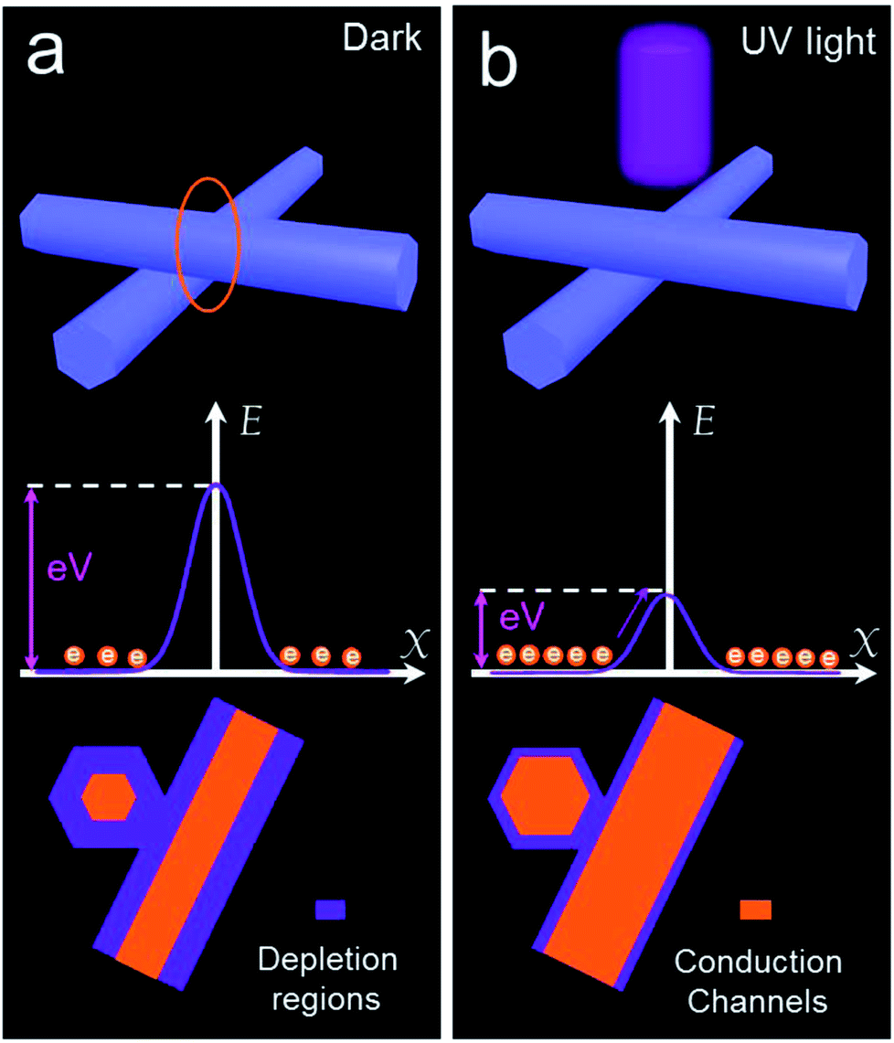 | ||
| Fig. 4 Schematic representation of (top) a close binding NWs network bridge (a) without or (b) under UV irradiation and its corresponding (middle) energy band diagram in the radial direction and (bottom) cross-section structural models. The middle schematics in (b) present a reduced potential barrier at the boundary of two close binding NWs in cross-section that are irradiated with UV light (bottom) significantly increased channel. | ||
Importantly, the NW network films can be integrated with wire-shaped substrates suitable for future wearable and smart devices, which can release part of bending stress and are suitable for wearable optoelectronic fields. A photograph of a ZnO NW network coated on KEVLAR exhibiting high flexibility is shown in Fig. 5a. The wire-shaped PD was fabricated by rolling a tensioning KEVLAR wire on the NW network substrates, which is illustrated in Fig. S6.† The film microstructure on the KEVLAR wire surface was characterized by SEM images (Fig. 5b and c). Similar to NW network films on planner substrates, the networks on wire-shaped substrates also exhibit high quality, crack-free, and smooth surfaces.
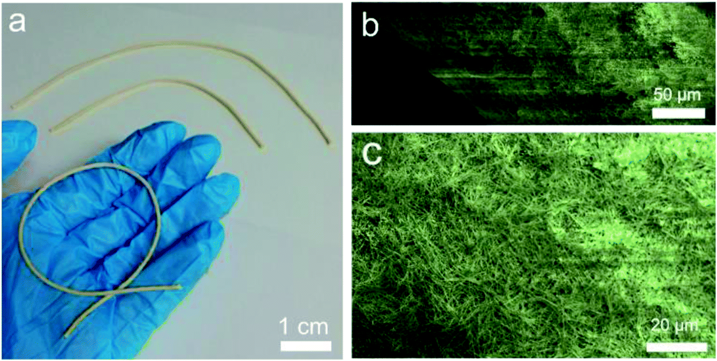 | ||
| Fig. 5 (a) Photograph of a ZnO NW network coated on wire-shaped KEVLAR. SEM image (b) and high magnification SEM image (c) of the ZnO NW network film coated on KEVLAR substrates. | ||
The NW networks on KEVLAR can be assembled into wire-shaped PDs by twining the CNT electrodes. The structure of a wire-shaped PD is demonstrated in Fig. 6a. The KEVLAR wire substrate is coated by ZnO NWs with CNTs as the electrode. The device's structure was confirmed by the SEM images shown in Fig. 6b and c. The contact between CNT and the ZnO NW network is good due to the excellent flexibility of CNT, which enables charge collecting from the NWs active layers.
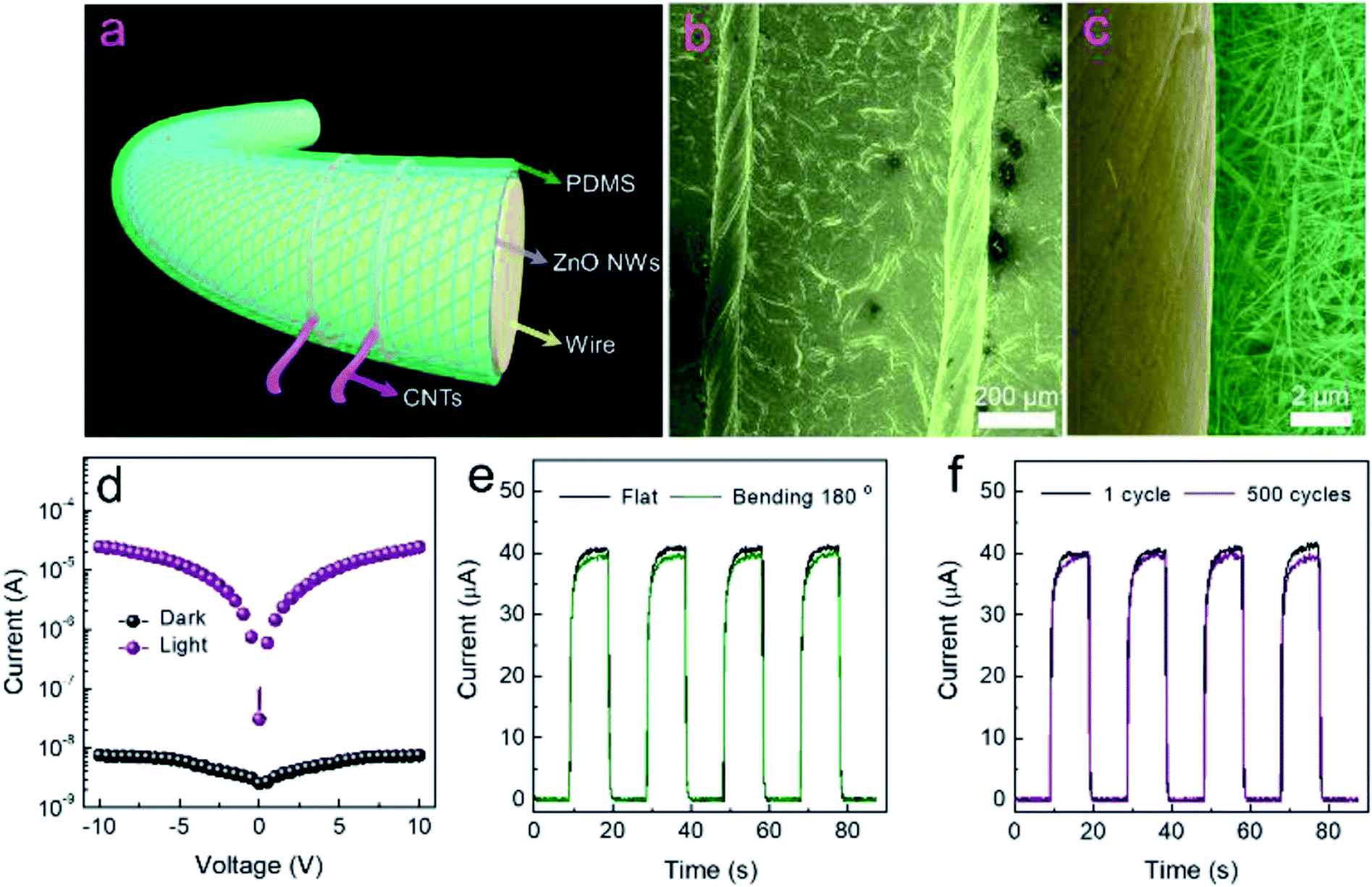 | ||
| Fig. 6 (a) Device structure of wire-shaped ZnO PD. (b) SEM image and (c) high magnification SEM image of wire-shaped ZnO PD. (d) I–V logarithm characteristics of ZnO wire-shaped NW PD in the dark and under 365 nm (0.35 mW cm−2) illumination. (e) I–t curves at 2 V of ZnO NW PD under 365 nm after bending and recovering cycles. (f) I–t curves at 2 V of ZnO NW PD under 365 nm with different cycle times. | ||
The wire-shaped PDs also exhibit high photoresponse features compared with those of a corresponding planner structure. As shown in Fig. 6d, the dark current and photocurrent for wire-shaped PDs are 4.7 nA and 5.71 μA at 2 V applied bias, respectively. The on/off current ratio was calculated to be 1.2 × 10³ at 2 V. Meanwhile, the wire-shaped PDs exhibited high flexibility. The photoresponse behavior of the device under different bending situations was characterized by measuring the current as a function of time when a 365 nm UV light was periodically turned on and off (Fig. S7†). The current–time (I–t) curves at 2 V bias under 365 nm laser (1 mW cm−2) under a flat conformation and bending 180° are respectively presented in Fig. 6e, with almost no change in the photocurrent value, which illustrates extraordinarily flexibility of our wire-shaped PDs. Additionally, after 500 cycles of bending tests, the I–t curves still remained at the same level (Fig. 6f). These good mechanical properties probably resulted from the network structure of ZnO NWs. SEM images of wire-shaped ZnO PD after bending for 500 times are illustrated in Fig. S8,† showing compactness and interconnecting NWs in the PD after 500 cycles without severe damage.
Importantly, the wire-shaped structure possesses excellent features such as less limitation of incident light angle, wider range of the substrate materials and wearability, and especially it can absorb light in incident directions and greatly diversified applications of PDs. The relationship between normalized responsivity and detecting angle is shown in Fig. 7. Obviously, the responsiveness of planar PDs decreases under side irradiation while the wire-shaped 360° PDs are capable of detecting incident directions and show no blind spots when compared with rigid planar structure PDs (Fig. 7b). Due to their unique structure, the performances (e.g., on/off ratio) of the 360° PDs remained almost unchanged under different bending angles with the same light intensity (Fig. 7c). Therefore, they can be efficiently used for wearable optoelectronic fields. Besides, a wire-shaped PD is also capable of long-time operating as the stability of Ilight vs. time demonstrated in Fig. S9† in which the photocurrent showed no decrease after 12 hours irradiation.
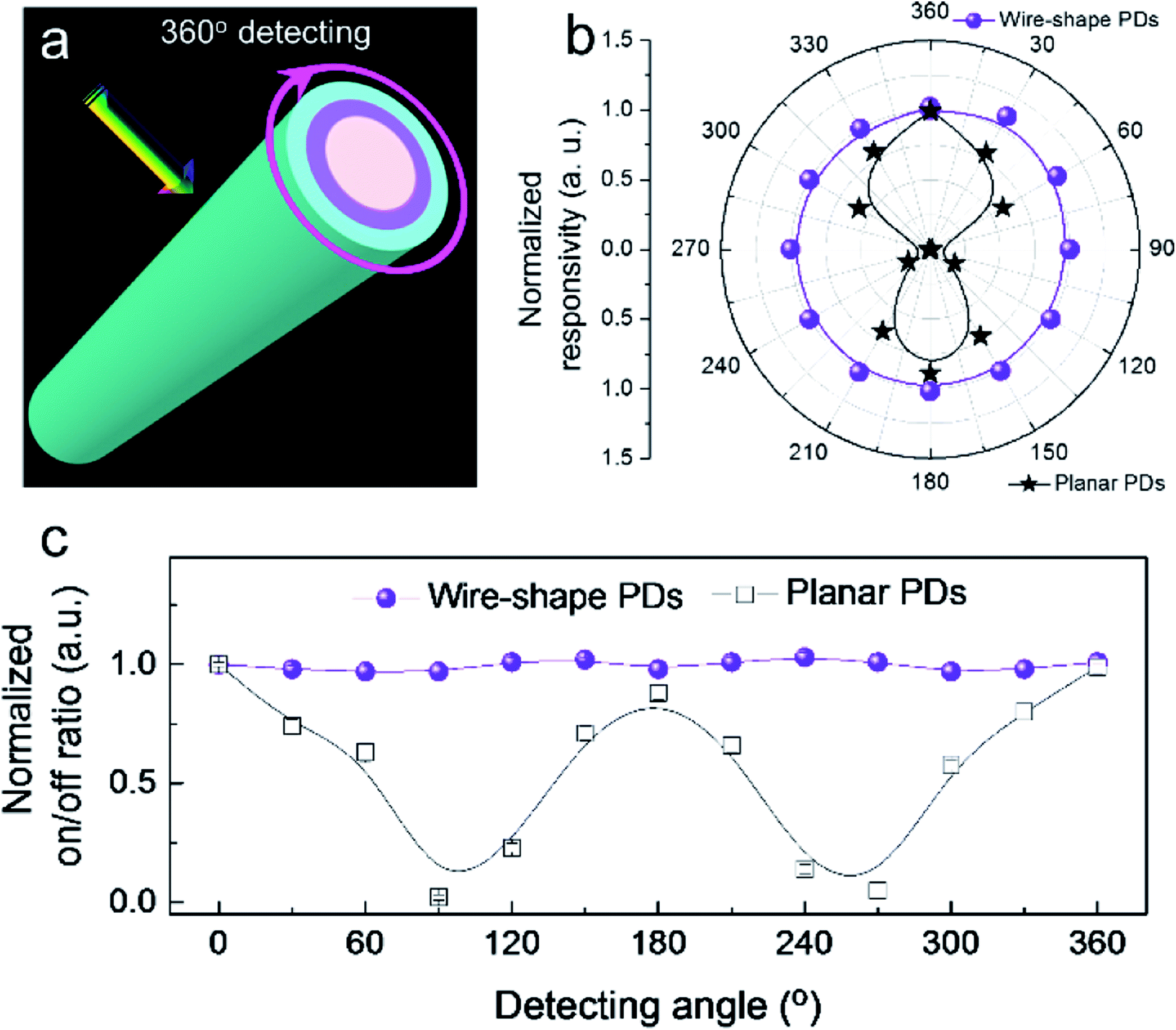 | ||
| Fig. 7 (a) Schematic of the 360° omnidirectional PDs. (b) Dependence of normalized responsibility for wire-shaped and planar PD at different detecting angles. (c) Dependence of on/off ratio and detecting angle for wire-shaped and planar PDs. | ||
Conclusions
In conclusion, we demonstrated highly flexible, omnidirectional PDs based on a ZnO NW network. PDs based on this NW network exhibit excellent performance with high-resolution imaging and an on/off ratio as high as about 104. Importantly, ZnO NW networks can be transferred onto wire-shaped substrates to construct omnidirectional PDs. As a result, wire-shaped PDs have excellent flexibility and a large light on/off ratio of 103. Besides, the omnidirectional PDs exhibit extraordinary stability against bending and irradiation. These results demonstrate a novel strategy for building wire-shaped optoelectronic devices through a NW network, which has high potential for future smart and wearable applications.Conflicts of interest
There are no conflicts to declare.Acknowledgements
We acknowledge Hehai Fang and Professor Weida Hu in Shanghai Institute of Technical Physics, Chinese Academy of Sciences for the support of photodetector imaging. This work was financially supported by the National Key Research and Development Program of China (2017YFA0305500, 2016YFB0401701), NSFC (61604074, 51572128, 51672132, 61725402), the Natural Science Foundation of Jiangsu Province (BK20160827, BK20180020), China Postdoctoral Science Foundation (2016M590455), the Fundamental Research Funds for the Central Universities (No. 30917011202, 30915012205, and 30916015106), and PAPD of Jiangsu Higher Education Institutions.Notes and references
- J. Zhong, Y. Zhang, Q. Zhong, Q. Hu, B. Hu, Z. L. Wang and J. Zhou, ACS Nano, 2014, 8, 6273–6280 CrossRef CAS PubMed.
- N. Yu, H. Yin, W. Zhang, Y. Liu, Z. Tang and M. Q. Zhu, Adv. Energy Mater., 2016, 6, 1501458 CrossRef.
- Z. Bao and X. Chen, Adv. Mater., 2016, 28, 4177–4179 CrossRef CAS PubMed.
- J. Xue, J. Song, Y. Dong, L. Xu, J. Li and H. Zeng, Sci. Bull., 2017, 62, 143–156 CrossRef CAS.
- Z. Zhang, K. Guo, Y. Li, X. Li, G. Guan, H. Li, Y. Luo, F. Zhao, Q. Zhang and B. Wei, Nat. Photonics, 2015, 9, 233 CrossRef CAS.
- Y. Dong, Y. Zou, J. Song, Z. Zhu, J. Li and H. Zeng, Nano Energy, 2016, 30, 173–179 CrossRef CAS.
- N. Nasiri, R. Bo, L. Fu and A. Tricoli, Nanoscale, 2017, 9, 2059–2067 RSC.
- Z. Zhu, Y. Gu, S. Wang, Y. Zou and H. Zeng, Adv. Electron. Mater., 2017, 3, 1700281 CrossRef.
- M. Qiu, P. Sun, Y. Liu, Q. Huang, C. Zhao, Z. Li and W. Mai, Adv. Mater. Technol., 2018, 3, 1700288 CrossRef.
- S. Pyo, W. Kim, H. I. Jung, J. Choi and J. Kim, Small, 2017, 13, 1700918 CrossRef PubMed.
- Y. Zhang, X. Q. Yan, Y. Yang, Y. H. Huang, Q. L. Liao and J. J. Qi, Adv. Mater., 2012, 24, 4647–4655 CrossRef CAS PubMed.
- P. Lin, X. Chen, X. Q. Yan, Z. Zhang, H. G. Yuan, P. F. Li, Y. G. Zhao and Y. Zhang, Nano Res., 2014, 7, 860–868 CrossRef CAS.
- S. Liu, Q. L. Liao, Z. Zhang, X. K. Zhang, S. N. Lu, L. X. Zhou, M. Y. Hong, Z. Kang and Y. Zhang, Nano Res., 2017, 10, 3476–3485 CrossRef CAS.
- Z. Zhang, Q. L. Liao, Y. H. Yu, X. D. Wang and Y. Zhang, Nano Energy, 2014, 9, 237–244 CrossRef CAS.
- T. Gao, Q. Zhang, J. Chen, X. Xiong and T. Zhai, Adv. Opt. Mater., 2017, 5, 1700206 CrossRef.
- N. Nasiri, R. Bo, F. Wang, L. Fu and A. Tricoli, Adv. Mater., 2015, 27, 4336–4343 CrossRef CAS PubMed.
- Y. H. Ko, G. Nagaraju and J. S. Yu, Nanoscale, 2015, 7, 2735–2742 RSC.
- Z. Zhu, D. Ju, Y. Zou, Y. Dong, L. Luo, T. Zhang, D. Shan and H. Zeng, ACS Appl. Mater. Interfaces, 2017, 9, 12092–12099 CrossRef CAS PubMed.
- X. Wang, K. Jiang and G. Shen, Mater. Today, 2015, 18, 265–272 CrossRef CAS.
- J. Chen, L. Ding, X. Zhang, L. Chu, N. Liu and Y. Gao, Opt. Express, 2014, 22, 3661–3668 CrossRef PubMed.
- H. Moon, H. Lee, J. Kwon, Y. D. Suh, D. K. Kim, I. Ha, J. Yeo, S. Hong and S. H. Ko, Sci. Rep., 2017, 7, 41981 CrossRef CAS PubMed.
- H.-G. Im, S.-H. Jung, J. Jin, D. Lee, J. Lee, D. Lee, J.-Y. Lee, I.-D. Kim and B.-S. Bae, ACS Nano, 2014, 8, 10973–10979 CrossRef CAS PubMed.
- J. Song, J. Li, J. Xu and H. Zeng, Nano Lett., 2014, 14, 6298–6305 CrossRef CAS PubMed.
- J. Song and H. Zeng, Angew. Chem., Int. Ed., 2015, 54, 9760–9774 CrossRef CAS PubMed.
- Y. Won, A. Kim, W. Yang, S. Jeong and J. Moon, NPG Asia Mater., 2014, 6, e132 CrossRef CAS.
- T. Cheng, Y. Zhang, W. Y. Lai and W. Huang, Adv. Mater., 2015, 27, 3349–3376 CrossRef CAS PubMed.
- K. K. Kim, S. Hong, H. M. Cho, J. Lee, Y. D. Suh, J. Ham and S. H. Ko, Nano Lett., 2015, 15, 5240–5247 CrossRef CAS PubMed.
- J. Song, S. A. Kulinich, J. Yan, Z. Li, J. He, C. Kan and H. Zeng, Adv. Mater., 2013, 25, 5750–5755 CrossRef CAS PubMed.
- J. Song, S. A. Kulinich, J. Li, Y. Liu and H. Zeng, Angew. Chem., 2015, 127, 472–476 CrossRef.
- G. Li, J. Zhang, G. Chen, H. Ye, X. Duan and X. Hou, Solid-State Electron., 2016, 123, 33–37 CrossRef CAS.
- J. Song, L. Xu, J. Li, J. Xue, Y. Dong, X. Li and H. Zeng, Adv. Mater., 2016, 28, 4861–4869 CrossRef CAS PubMed.
- L. Li, P. Wu, X. Fang, T. Zhai, L. Dai, M. Liao, Y. Koide, H. Wang, Y. Bando and D. Golberg, Adv. Mater., 2010, 22, 3161–3165 CrossRef CAS PubMed.
- N. Guo, W. Hu, T. Jiang, F. Gong, W. Luo, W. Qiu, P. Wang, L. Liu, S. Wu and L. Liao, Nanoscale, 2016, 8, 16065–16072 RSC.
- M. Engel, M. Steiner and P. Avouris, Nano Lett., 2014, 14, 6414–6417 CrossRef CAS PubMed.
- D. K. Hwang, Y. T. Lee, H. S. Lee, Y. J. Lee, S. H. Shokouh, J.-h. Kyhm, J. Lee, H. H. Kim, T.-H. Yoo and S. H. Nam, NPG Asia Mater., 2016, 8, e233 CrossRef CAS.
- C. Y. Yan, N. Singh and P. S. Lee, Appl. Phys. Lett., 2010, 96, 044507 Search PubMed.
- M. R. Alenezi, S. J. Henley and S. Silva, Sci. Rep., 2015, 5, 8516 CrossRef PubMed.
- J. Wang, C. Yan, M.-F. Lin, K. Tsukagoshi and P. S. Lee, J. Mater. Chem. C, 2015, 3, 596–600 RSC.
- Z. Zhan, L. Xu, J. An, H. Du, Z. Weng and W. Lu, Adv. Eng. Mater., 2017, 19, 1700101 CrossRef.
- G. Cheng, X. H. Wu, B. Liu, B. Li, X. T. Zhang and Z. L. Du, Appl. Phys. Lett., 2011, 99, 203105 CrossRef.
Footnote |
| † Electronic supplementary information (ESI) available. See DOI: 10.1039/c8ra06555a |
| This journal is © The Royal Society of Chemistry 2018 |