
 Open Access Article
 This Open Access Article is licensed under a Creative Commons Attribution-Non Commercial 3.0 Unported Licence
Epitaxial growth and interfacial property of monolayer MoS2 on gallium nitride
Pengfei Yanab,
Qianqian Tianb,
Guofeng Yang *b,
Yuyan Weng*a,
Yixin Zhangb,
Jin Wangb,
Feng Xiec and
Naiyan Lua
*b,
Yuyan Weng*a,
Yixin Zhangb,
Jin Wangb,
Feng Xiec and
Naiyan Lua
aState Key Laboratory of Food Science and Technology, Jiangnan University, Wuxi 214122, China. E-mail: wengyuyan@suda.edu.cn
bSchool of Science, Jiangsu Provincial Research Center of Light Industrial Optoelectronic Engineering and Technology, Jiangnan University, Wuxi 214122, China. E-mail: gfyang@jiangnan.edu.cn
cNanjing Zike Optoelectronic Co., Ltd, Nanjing 211112, China
First published on 25th September 2018
Abstract
Two-dimensional (2D) transition-metal dichalcogenides (TMDCs) on semiconductor substrates are important for next-generation electronics and optoelectronics. In this study, we demonstrate the growth of monolayer MoS2 on a lattice-matched gallium nitride (GaN) semiconductor substrate by chemical vapor deposition (CVD). The monolayer MoS2 triangles exhibit optical properties similar to that of typical single-crystal MoS2 sheets, as verified by the Raman, photoluminescence, and morphological characterizations. The Raman and PL features and their intensity mappings suggest that the as-grown MoS2 on GaN substrate can achieve high quality and uniformity, demonstrating that GaN substrate is favorable for 2D MoS2 growth. Moreover, the interfacial property and stacking structure were investigated by first-principles density functional theory (DFT) calculations to confirm the interlayer interactions of monolayer MoS2 on GaN. Accordingly, the ability to grow high quality monolayer MoS2 on semiconductor GaN substrate would open a new route toward the synthesis of hetero and composite structures for promising electronic and optoelectronic device applications.
1. Introduction
The most investigated member of the two-dimensional (2D) transition-metal dichalcogenide (TMD) materials, monolayer molybdenum disulfide (MoS2), has attracted widespread attention for a variety of next-generation electrical and optoelectronic devices applications due to its atomically sharp interfaces, ultrathin dimensions, flexibility and large optical effects.1,2 The proof-of-concept ultrafast field-effect transistors (FETs), optical devices, and flexible electronics3–5 based on 2D MoS2 have been investigated. In general, at the beginning, the 2D MoS2 applied on these devices was obtained by exfoliation of geological MoS2 crystals and mechanically transferred to the desired substrates. However, small specimen sizes, uncertainty in placement location, and lack of composition control are the main drawbacks for the applications of geological MoS2.6 In order to overcome these limitations, many methods have been used to grow the 2D materials with engineered composition. 2D MoS2 has been synthesized by chemical vapor deposition (CVD),7 metal–organic chemical vapor deposition (MOCVD),8 and pulsed laser deposition (PLD).9 In most of these reports, monolayer MoS2 has been primarily grown on SiO2 substrate, which resulted in the random orientation of MoS2 domains and grain boundaries because of the amorphous nature of the substrate and its relatively high surface roughness.10Moreover, the growth and fabrication of thin-film devices on semiconductor wafers constitute the bulk of the semiconductor industry.11 Thus, the growth of high-quality 2D materials on semiconductor substrates would have technological advantages and broad applications. Considerable progress has been made on the growth of 2D MoS2,12 MoSe2,13 WS2,14 WSe2,15 and black phosphorene16 on insulating substrates of SiO2 and other compounds. Dumcenco et al. reported the successful growth of single-domain and large monolayer MoS2 films on c-sapphire substrates.17 Growth of monolayer MoS2 on an inert and nearly lattice-matching mica substrate by using a low-pressure chemical vapor deposition method was successfully demonstrated.18 Although these growth techniques are well established, the resulting 2D materials still need to be transferred to some unique semiconducting substrate surfaces to be integrated into the microelectronic or optoelectronic technologies for special functions. In fact, transfer processes19 would consume additional time and cause severe interfacial defects. Hence, the direct growth of 2D materials on semiconducting wafers or films can overcome these problems and result in ideal quality films. Many attempts have been made to grow 2D materials directly on semiconducting substrates, including Si,20 GaAs,21 SiC,22 and others,23 and preliminary hetero-junction devices have been fabricated. However, due to the unfavorable lattice mismatches, the domain orientation and size uniformity are not yet satisfactory. In contrast, the 2D material growth on more suitable semiconductor substrates may potentially offer better crystal quality. For example, the growth of MoS2 on c-plane GaN substrate offers better crystal quality because the hexagonally symmetric GaN surface matches well with MoS2. The c-plane lattice constants of GaN and MoS2 are a = 3.18 Å and 3.16 Å, respectively, corresponding to a small mismatch of 2%. Moreover, the commonly used Ga-polar GaN substrate is uniformly terminated with Ga2+ cations, which facilitate the adsorption of S anions and the growth of smooth S–Mo–S layers. Therefore, it is particularly interesting to grow 2D MoS2 on GaN substrate due to their close lattice match and favorable electronic band structure alignment for electronic and optoelectronic device requirements.
In this study, monolayer MoS2 has been grown on a lattice-matched GaN semiconductor substrate by CVD method. Accordingly, triangle single-layer MoS2 domains were commonly observed on the GaN substrate, and the excitation laser power dependent PL and Raman spectra were characterized to investigate the optical property of monolayer MoS2 on GaN. Moreover, uniform color contrast of the PL and Raman intensity mappings suggest that the as-grown triangular monolayer MoS2 on GaN substrate are of high quality and uniformity. Finally, first-principles density functional theory (DFT) calculations were employed to investigate the interfacial property and interactions of monolayer MoS2 on semiconductor GaN.
2. Methods
Growth procedure
Monolayer MoS2 was grown by CVD on the (0001) plane of GaN substrate. The substrate was cleaned by an ultrasonic cleaner with acetone, absolute ethyl alcohol, and deionized water. Following this, they were placed face-down on a crucible containing ∼0.1 g of MoO3 (99.9%) and loaded into a CVD heating furnace (downstream) with a 60 mm outer diameter quartz tube. CVD growth was performed at atmospheric pressure using ultra-high-purity N2 as the carrier gas. A second crucible containing 1 g of sulfur powder (99.9% purity) was located in another heating zone, which was upstream from the growth substrate. Pure N2 gas was first introduced into the CVD furnace with a flow rate of 100 sccm for 20 min to purge the tube and then maintained at a flow rate of 50 sccm during the entire growth process. During the heating process, the downstream heating zone was initially heated to 800 °C in 120 min, while the upstream heating zone was first maintained at room temperature for 70 min and then heated to 200 °C in 50 min, ensuring that the sulfur powder was sufficiently evaporated when the MoO3 powder was heated to 800 °C. Consequently, the growth temperature was maintained at 800 °C for 15 min, and then naturally cooled down to room temperature in 2 h.Characterization
The surface morphologies and thicknesses of the as-grown MoS2 on GaN substrate were characterized by optical microscope, field emission scanning electron microscope (FE-SEM: JEOL JSM-7000F) and atomic force microscope (AFM: Bruker Dimension ICON). The Raman and photoluminescence (PL) characterizations were performed using a Renishaw LabRAM Inviamicro-Raman system using a 532 nm excitation laser at room temperature, with laser spot size set at about 1 μm using a 50× objective.Density functional theory modelling
First-principles calculations based on density functional theory (DFT) were employed to study the interfacial and electronic structure properties of monolayer MoS2 on GaN (0001) plane. ATOMISTIX TOOLKIT (ATK) code was used in implementing the calculations.24 It is well known that the band gaps calculated at generalized gradient approximation (GGA) level are usually underestimated compared with the experimental values for some materials. To ensure the accuracy of the simulations, we optimized the structures of the MoS2–GaN system by using Perdew–Burke–Ernzerhof (PBE) of GGA25 for the exchange–correlation functional together with the SG15 pseudopotentials. The structure was optimized using the limited-memory Broyden–Fletcher–Goldfarb–Shanno (LBFGS) scheme till the forces on individual atoms were mitigated to less than 0.05 eV Å−1 and the stress error tolerance was less than 0.1 GPa. To take the van der Waals (vdW) interaction into account, the Grimme's DFT-D2 dispersion-correction approach was adopted for all exchange correlation energies due to its higher accuracy and less empiricism.26 A well-conserved 9 × 9 × 1 k-point mesh was used for the structure optimization and electronic structure calculation with a density mesh cutoff energy of 75 Hartree. The buffer space of a vacuum of 20 Å was set to eliminate the coupling between two adjacent units. In the calculation, six atomic layers of GaN were chosen for the interface simulations since the obtained results do not change appreciably beyond this thickness, where the method has been widely used previously.3. Results and discussion
Fig. 1(a) shows the optical microscopy image of MoS2 grown on GaN substrate. As the GaN substrate is grown by MOCVD, the dislocation density on the substrate surface is as low as 10−7 cm−3,27 which can be neglected between the interface of GaN and as-grown MoS2 domain. It can be clearly seen that some of the as-grown MoS2 domains are triangular with uniform color contrast, where the lateral sizes have a certain limit due to the high energy caused by the lattice mismatch between the MoS2 and the substrates. To confirm the thickness of the obtained MoS2 films, a typical AFM image shown in Fig. 1(b) presents the edge of a triangular MoS2 domain on the GaN substrate. The height profile taken from the solid line in Fig. 1(b) reveals a film thickness of 0.8 nm, which is consistent with the range of a single-layered MoS2 film on bare substrates (other than GaN substrate, 0.6–0.9 nm) grown by CVD,28,29 demonstrating that the monolayer MoS2 has been successfully obtained by the growth procedure on GaN substrate. Fig. 1(d) presents the SEM images of the as-grown monolayer MoS2 on GaN, which indicate that most of the MoS2 domains are monolayer single crystal, with large coverage ratio on the substrate. Additionally, it can be observed from the inset of the enlarged SEM image in Fig. 1(d) that the lateral size of the largest single triangular MoS2 domain reaches as high as 50 μm on the GaN substrate.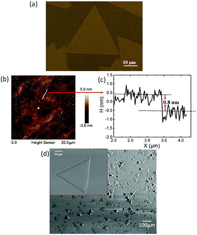 | ||
| Fig. 1 (a) Optical microscopy image, (b) AFM image, (c) the corresponding height profile, and (d) SEM images of the as-grown MoS2 on GaN substrate. | ||
Fig. 2(a) shows the Raman spectra of triangular MoS2 domain at room temperature. Typical peak positions of in-plane E12g (∼383 cm−1) and out-of-plane A1g (∼402 cm−1) Raman modes of the vibrations in MoS2 can be clearly observed. The wave number difference between the E12g and A1g peaks estimated from the Raman spectra is less than 19 cm−1, identifying that the thickness of the as-grown MoS2 nanosheet is single layer.30 The behaviors as a function of excitation laser power (with the maximum excitation laser power denoted as P0) imply that the E12g vibration changes slightly, while the A1g vibration softens (red shifts) from 385.7 cm−1 to 403.25 cm−1 with the increase in the excitation power. The powers of the excitation laser lines are maintained well below 1 mW to avoid heating effects. The red-shift suggests that van der Waals force plays a minor role, while stacking-induced structure changes and long-range coulombic interlay interactions may dominate the change in atomic vibrations within MoS2 on GaN substrate.30 Fig. 2(b) depicts the room-temperature PL spectra of monolayer MoS2 grown on GaN as a function of excitation laser power. It is notable that the emission peak excited by the lowest laser power is located at ∼674 nm, further demonstrating the single-layer feature of the as-grown MoS2 on GaN.18 Additionally, only strikingly strong PL of A peak exciton, with no shoulder peak of B peak exciton is observed from Fig. 2(b). Such a single PL peak feature has been reported in exfoliated monolayer MoS2 suspended on holed Si substrate.31 Hence, the observation of a single (A excitonic emission) peak is a strong evidence that the monolayer MoS2 grown herein on GaN substrate is undoubtedly of high quality.18 Moreover, it is observed that the PL peaks of MoS2 on GaN substrate exhibit slight shift as the excitation laser intensity increases, indicating that possible heating effect caused by increasing laser power can be excluded. It can also be derived that the full width at half-maximum (FWHM) of the PL spectra for MoS2 on GaN exhibits no apparent broadening, demonstrating that GaN substrate is favorable for 2D MoS2 growth due to its lattice-match feature and the appropriate thermal conductivity of the GaN substrate.
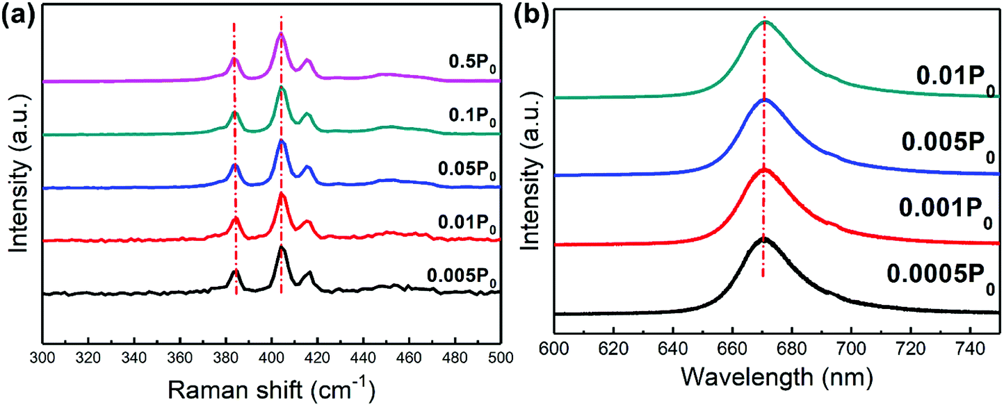 | ||
| Fig. 2 Normalized Raman spectra (a) and PL spectra (b) of monolayer MoS2 on GaN as a function of excitation laser power. | ||
In order to further investigate the uniformity of monolayer triangular MoS2 domains on the GaN substrate, Fig. 3(a) and (b) present the Raman intensity mappings at 383 cm−1 and 402 cm−1, respectively, from which uniform color distribution and strong intensity can be observed in all the positions of the single triangular domain. Furthermore, the PL intensity mappings of MoS2 on GaN at a wavelength of 674 nm (shown in Fig. 3(c)) also exhibits very uniform color contrast across the entire surface, with a small discrepancy at the very edge of the triangle domain, which would have been caused by the partial absorption of the laser spot energy. Such a uniformity of the PL and Raman intensity mappings over the entire surface further suggests that the as-grown triangular monolayer MoS2 on GaN substrate is of high quality with a low presence of defects. The low presence of defects is beneficial because local defects may easily absorb water vapor and oxygen molecules in the air and thus affect the PL and Raman intensities locally, which might lead to inhomogeneity of PL and Raman intensities, as proved by previous studies.32
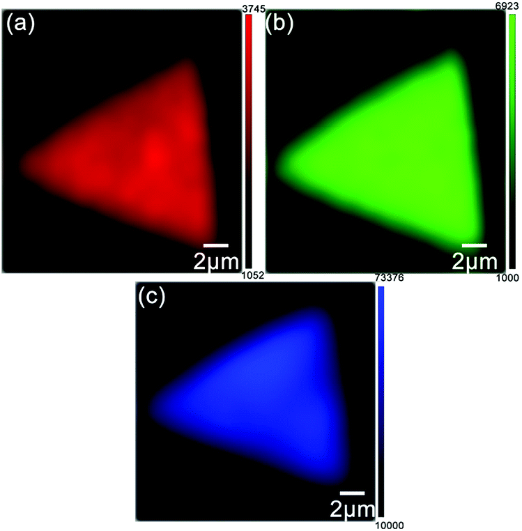 | ||
| Fig. 3 Raman peak intensity mapping at 383 cm−1 (a) and 402 cm−1 (b), and PL peak intensity mapping at 674 nm (c) of monolayer MoS2 on GaN substrate. | ||
First-principles calculations based on density functional theory (DFT) were performed to investigate the interfacial property and stacking structure and confirm the interlay interactions of monolayer MoS2 on GaN. Fig. 4 shows the electronic band structure of the bare monolayer MoS2 calculated in a primitive unit cell. It can be seen that the maximum of the valence band and the minimum of the conduction band appear at the same point, indicating a direct band gap Eg = 1.8 eV, which is consistent with the PL emission peak value in our experimental results, as mentioned above and in other reported results,28,33 thus verifying the accuracy of the optimized atomic configurations.
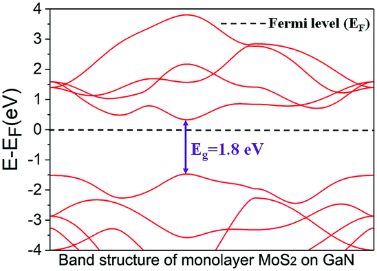 | ||
| Fig. 4 The band structure of bare monolayer MoS2 calculated in a primitive unit cell. | ||
Fig. 5(a) shows the top view and side view of the optimized structure of monolayer MoS2 and GaN substrate, and the electronic band structure of the interfacial system is shown in Fig. 5(b). It can be clearly seen that the growth of MoS2 on GaN does not significantly perturb the band structure and only brings about a very small band gap change. New electronic bands below −0.5 eV are introduced after the monolayer MoS2 adsorption, while most bands of the interfacial MoS2–GaN system retain the nature of original GaN bands, and the band gap does not change considerably. These results demonstrate that the growth of monolayer MoS2 on the GaN surface would not make significant changes on the interfacial property of GaN, and the calculated binding energy of monolayer MoS2 and (0001) GaN is as low as 0.0993 eV.
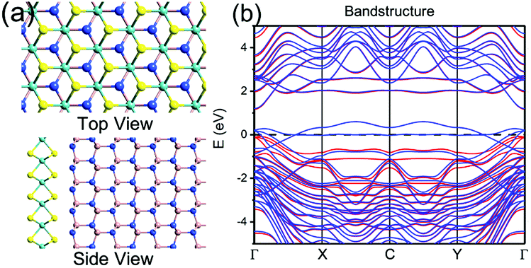 | ||
| Fig. 5 (a) Top view and side view of the atomic structure of MoS2 on GaN. (b) The electronic band structure of the interfacial MoS2–GaN system. | ||
Furthermore, the average electron density plot along the monolayer MoS2–GaN system is depicted in Fig. 6(a). The value of the electron density provides a visual and quantitative evaluation of the interfacial interactions. Higher electron density at the interface indicates higher interfacial interactions. The minimum value of electron density at the interface is 0.135 Å−3 for the MoS2–GaN system, indicating a low van der Waals force at the interface. Thus, the MoS2 overlayers are not expected to show much strain because of their weak vdW interactions with the substrate. Furthermore, the electron localization function of the monolayer MoS2–GaN system is displayed in Fig. 6(b) in order to estimate the bonding nature between MoS2 and GaN substrate. It can be noted that the electron localization function indicates that electrons localize inside the GaN and MoS2 layers instead of the interlayer space, suggesting the weak van der Waals force between the two layers. From this finding, we can conclude that the weak van der Waals force plays a minor role on the atomic vibration at the interface between monolayer MoS2 and GaN, which is in agreement with the abovementioned experimental findings.
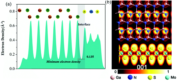 | ||
| Fig. 6 (a) The average electron density in planes normal to the monolayer MoS2–GaN interface. (b) The electron localization function (ELF) of the monolayer MoS2–GaN geometrical structure. | ||
4. Conclusion
In conclusion, we have achieved epitaxial chemical vapor deposition growth of monolayer MoS2 on a GaN semiconductor substrate. High crystalline quality and uniformity of the as-grown monolayer MoS2 is demonstrated by their Raman and PL features and their intensity mappings, suggesting that GaN substrate is favorable for 2D MoS2 growth. Moreover, laser power dependent Raman and PL characterizations were performed to investigate the optical and atomic vibration properties of MoS2 on GaN. The relatively weak van der Waals interaction controls the crystalline growth and plays a minor role on the atomic vibration, which was explored and confirmed by interfacial structure and interaction investigations between monolayer MoS2 and GaN substrate based on the first-principles density functional theory calculations. As a result, the ability to grow high quality monolayer MoS2 on semiconductor GaN substrate would open a route toward the synthesis of hetero and composite structures for electronic and optoelectronic device applications.Conflicts of interest
The authors declare no competing financial interest.Acknowledgements
This study was supported by the National Natural Science Foundation of China (No. 11604124, 61604080, 61504050), Open Project Program of State Key Laboratory of Food Science and Technology, Jiangnan University (No. SKLF-KF-201706), Natural Science Foundation of Jiangsu Province (No. BK20150158, BM2014402), the Fundamental Research Funds for Central Universities (No. JUSRP51628B, JUSRP51517, JUSRP51716A), National First-Class Discipline Program of Food Science and Technology (No. JUFSTR20180302), University Science Research Project of Jiangsu Province (Grant No. 16KJB140011).Notes and references
- A. K. Geim and I. V. Grigorieva, Nature, 2013, 499, 419–425 CrossRef PubMed.
- H. Jeong, S. Bang, H. M. Oh, H. J. Jeong, S.-J. An, G. H. Han, H. Kim, K. K. Kim, J. C. Park, Y. H. Lee, G. Lerondel and M. S. Jeong, ACS Nano, 2015, 9, 10032–10038 CrossRef PubMed.
- D. Krasnozhon, D. Lembke, C. Nyffeler, Y. Leblebici and A. Kis, Nano Lett., 2014, 14, 5905–5911 CrossRef PubMed.
- K. F. Mak, K. He, J. Shan and T. F. Heinz, Nat. Nanotechnol., 2012, 7, 494–498 CrossRef PubMed.
- G.-H. Lee, Y.-J. Yu, X. Cui, N. Petrone, C.-H. Lee, M. S. Choi, D.-Y. Lee, C. Lee, W. J. Yoo, K. Watanabe, T. Taniguchi, C. Nuckolls, P. Kim and J. Hone, ACS Nano, 2013, 7, 7931–7936 CrossRef PubMed.
- E. Varrla, C. Backes, K. R. Paton, A. Harvey, Z. Gholamvand, J. McCauley and J. N. Coleman, Chem. Mater., 2015, 27, 1129–1139 CrossRef.
- H. Liu, M. W. Si, S. Najmaei, A. T. Neal, Y. C. Du, P. M. Ajayan, J. Lou and P. D. D. Ye, Nano Lett., 2013, 13, 2640–2646 CrossRef PubMed.
- K. Kang, S. Xie, L. Huang, Y. Han, P. Y. Huang, K. F. Mak, C.-J. Kim, D. Muller and J. Park, Nature, 2015, 520, 656–660 CrossRef PubMed.
- C. R. Serrao, A. M. Diamond, S.-L. Hsu, L. You, S. Gadgil, J. Clarkson, C. Carraro, R. Maboudian, C. Hu and S. Salahuddin, Appl. Phys. Lett., 2015, 106, 052101 CrossRef.
- O. V. Yazyev and Y. P. Chen, Nat. Nanotechnol., 2014, 9, 755–767 CrossRef PubMed.
- L. J. Van Ruyven, J. Lumin., 1984, 29, 123–161 CrossRef.
- Q. H. Wang, K. Kalantar-Zadeh, A. Kis, J. N. Coleman and M. S. Strano, Nat. Nanotechnol., 2012, 7, 699–712 CrossRef PubMed.
- H. Heo, J. H. Sung, G. Jin, J. H. Ahn, K. Kim, M. J. Lee, S. Cha, H. Choi and M. Jo, Adv. Mater., 2015, 27, 3803–3810 CrossRef PubMed.
- H. R. Gutiérrez, N. Perea-Lopez, A. L. Elias, A. Berkdemir, B. Wang, R. Lv, F. Lopez-Urias, V. H. Crespi, H. Terrones and M. Terrones, Nano Lett., 2013, 13, 3447–3454 CrossRef PubMed.
- B. Liu, M. Fathi, L. Chen, A. Abbas, Y. Ma and C. Zhou, ACS Nano, 2015, 9, 6119–6127 CrossRef PubMed.
- L. K. Li, Y. Yu, G. J. Ye, Q. Ge, X. Ou, H. Wu, D. Feng, X. H. Chen and Y. Zhang, Nat. Nanotechnol., 2014, 9, 372–377 CrossRef PubMed.
- D. Dumcenco, D. Ovchinnikov, K. Marinov, P. Lazic, M. Gilbertini, N. Marzari, O. L. Sanchez, Y. C. Kung, D. Krasnozhon, M. W. Chen, S. Bertolazzi, P. Gillet, A. F. I. Morral, A. Radenovic and A. Kis, ACS Nano, 2015, 9, 4611–4620 CrossRef PubMed.
- Q. Q. Ji, Y. F. Zhang, T. Gao, Y. Zhang, D. L. Ma, M. X. Liu, Y. B. Chen, X. F. Qiao, P. H. Tan, M. Kan, J. Feng, Q. Sun and Z. F. Liu, Nano Lett., 2013, 13, 3870–3877 CrossRef PubMed.
- Z. Lin, Y. Zhao, C. Zhou, R. Zhong, X. Wang, Y. H. Tsang and Y. Chai, Sci. Rep., 2015, 5, 18596 CrossRef PubMed.
- Y. Liu, L. Hao, W. Gao, Z. Wu, Y. Lin, G. Li, W. Guo, L. Yu, H. Zeng, J. Zhu and W. Zhang, Sens. Actuators, B, 2015, 211, 537–543 CrossRef.
- S. Lin, X. Li, P. Wang, Z. Xu, S. Zhang, H. Zhong, Z. Wu, W. Xu and H. Chen, Sci. Rep., 2015, 5, 15103 CrossRef PubMed.
- E. W. Lee, L. Ma, D. N. Nath, C. H. Lee, A. Arehart, Y. Wu and S. Rajan, Appl. Phys. Lett., 2014, 105, 203504 CrossRef.
- S. Vishwanath, X. Liu, S. Rouvimov, P. C. Mende, A. Azcatl, S. McDonnell, R. M. Wallace, R. M. Feenstra, J. K. Furdyna, D. Jena and H. G. Xing, 2D Mater., 2015, 2, 024007 CrossRef.
- J. Taylor, H. Guo and J. Wang, Phys. Rev. B: Condens. Matter Mater. Phys., 2001, 63, 121104 CrossRef.
- J. P. Perdew, K. Burke and M. Ernzerhof, Phys. Rev. Lett., 1996, 77, 3865–3868 CrossRef PubMed.
- S. Grimme, J. Antony, S. Ehrlich and H. Krieg, J. Chem. Phys., 2010, 132, 154104 CrossRef PubMed.
- G. F. Yang, P. Chen, Z. L. Wu, Z. G. Yu, H. Zhao, B. Liu, X. M. Hua, Z. L. Xie, X. Q. Xiu, P. Han, Y. Shi, R. Zhang and Y. D. Zheng, J. Mater. Sci.: Mater. Electron., 2012, 23, 1224–1228 CrossRef.
- B. Radisavljevic, A. Radenovic, J. Brivio, V. Giacometti and A. Kis, Nat. Nanotechnol., 2011, 6, 147–150 CrossRef PubMed.
- A. Splendiani, L. Sun, Y. B. Zhang, T. S. Li, J. Kim, C. Y. Chim, G. Galli and F. Wang, Nano Lett., 2010, 10, 1271–1275 CrossRef PubMed.
- C. Lee, H. Yan, L. E. Brus, T. F. Heinz, J. Hone and S. Ryu, ACS Nano, 2010, 4, 2695–2700 CrossRef PubMed.
- K. F. Mak, C. Lee, J. Hone, J. Shan and T. F. Heinz, Phys. Rev. Lett., 2010, 105, 136805 CrossRef PubMed.
- H. Nan, Z. L. Wang, W. H. Wang, Z. Liang, Y. Lu, Q. Chen, D. W. He, P. H. Tan, F. Miao, X. R. Wang, J. L. Wang and Z. H. Ni, ACS Nano, 2014, 8, 5738–5745 CrossRef PubMed.
- Y. H. Lee, L. L. Yu, H. Wang, W. J. Fang, X. Ling, Y. M. Shi, C. T. Lin, J. K. Huang, M. T. Chang, C. S. Chang, M. Dresselhaus, T. Palacios, L. J. Li and J. Kong, Nano Lett., 2013, 13, 1852–1857 CrossRef PubMed.
| This journal is © The Royal Society of Chemistry 2018 |