
 Open Access Article
 This Open Access Article is licensed under a Creative Commons Attribution-Non Commercial 3.0 Unported Licence
Reducing series resistance in Cu2ZnSn(S,Se)4 nanoparticle ink solar cells on flexible molybdenum foil substrates†
Xinya Xu ,
Yongtao Qu,
Vincent Barrioz,
Guillaume Zoppi and
Neil S. Beattie*
,
Yongtao Qu,
Vincent Barrioz,
Guillaume Zoppi and
Neil S. Beattie*
Department of Mathematics, Physics and Electrical Engineering, Northumbria University, Newcastle-upon-Tyne, NE1 8ST, UK. E-mail: neil.beattie@northumbria.ac.uk
First published on 17th January 2018
Abstract
Earth abundant Cu2ZnSnS4 nanoparticle inks were deposited on molybdenum foil substrates and subsequently converted to high quality thin film Cu2ZnSn(S,Se)4 photovoltaic absorbers. Integration of these absorbers within a thin film solar cell device structure yields a solar energy conversion efficiency which is comparable to identical devices processed on rigid glass substrates. Importantly, this is only achieved when a thin layer of molybdenum is first applied directly to the foil. The layer limits the formation of a thick Mo(S,Se)x layer resulting in a substantially reduced series resistance.
Introduction
Cu2ZnSn(S,Se)4 (CZTSSe) is considered a promising photovoltaic absorber material due to its high theoretical power conversion efficiency, ideal direct energy band-gap for solar light conversion and large absorption coefficient in the visible range.1,2 Recently, Solar Frontier achieved a new world record Cu(In,Ga)Se2 (CIGS) thin-film solar cell efficiency of 22.9%,3 however, it contains In and Ga, limiting its wide application. The related absorber material CZTS contains only earth-abundant elements and it is relatively low-cost, making it suitable for large area manufacture.4 In addition, fabrication on flexible substrates has the potential to create lightweight solar cells that offer a wide range of application, such as roll-to-roll manufacturing and integration on a variety of surfaces including automotive and buildings. The high power-to-mass ratio of flexible solar cells further favour the applications on both space and ground utilities.5 Inorganic photovoltaic technologies are generally recognized for their operational stability. In addition, nearly all of them require high temperature treatment during the fabrication and this is a particular advantage of using molybdenum foil as a substrate as it is compatible with the high temperatures (>500 °C) required to form large grains in a thin film photovoltaic absorber. CZTSSe solar cells on rigid glass substrates using hydrazine processing have achieved efficiency as high as 12.6%,6 while CZTSSe solar cells based on less hazardous nanoparticle inks have also reached 9.3%.7 However, research on Cu2ZnSnS4 (CZTS) nanoparticle inks on flexible substrates is still comparatively limited with the highest reported efficiency of 6.1% additionally with MoNa and Ge doping.8There are several promising substrate candidates for flexible CZTS and CZTSSe solar cells including stainless steel8,9 and glass.10 In choosing a suitable flexible substrate, the coefficient of thermal expansion (CTE), surface smoothness, and chemical inertness should be taken consideration.11 Molybdenum (Mo) foil has the advantage over polymers in that it is robust to high temperature processing however, in an important work, Zhang et al. report degradation of the device performance stemming from high series resistance (Rs).12
Among the landscape of research on flexible substrates, there are currently no reports of CZTSSe solar cells on Mo foils. In this work we show that CZTSSe solar cells from CZTS nanoparticle inks can be fabricated directly on commercially available Mo foil substrates. Furthermore, we demonstrate that the origin of high Rs is a consequence of a thick Mo(S,Se)x that forms between the foil substrate and the photovoltaic absorber. This can be overcome via the application of a thin sputtered Mo layer on the foil resulting in values of Rs which are the same as those for identical solar cells built on rigid glass substrates.
Experimental details
Mo foil (99.9%, Sigma Aldrich) was chosen as the flexible substrate, due to its thermal stability and high conductivity. The CTE for molybdenum is approximately 5.5 × 10⁻⁶ K−1 in the range 25–500 °C (ref. 13) which is slightly lower than the CTE for soda lime glass (SLG). The dimensions of the Mo foil substrate were cut to be 25 mm × 25 mm × 0.1 mm. The flexible substrates were prepared in two different ways: one was the bare Mo foil with corresponding resistivity of 5.0 μΩ cm; while the other was the Mo foil coated with an 800 nm thick Mo film with similar resistivity to bare Mo foil. Additionally, an SLG rigid substrate was used for comparison purposes with dimensions 25 mm × 25 mm × 1 mm and coated with a 800 mm thick Mo film with resistivity of 50.7 μΩ cm.The Mo films on SLG and Mo film were sputtered by direct current magnetron sputtering with target power density of 9 mW cm−2 and argon pressure of 7 mTorr at room temperature. Surface roughness (Ra) of the substrates as measured by atomic force microscope (AFM) were 3.30 nm, 3.15 nm and 2.18 nm for foil, foil with sputtered Mo film and Mo coated glass substrates, respectively (see Fig. S1 in the ESI†).
Solar cell devices fabricated on these substrates had the following structure: substrate/(Mo film/)CZTSSe/CdS/ZnO/ITO/Ni/Al, where ITO denotes indium tin oxide. Initially, CZTS nanoparticles were fabricated by injection of metallic precursors into a hot surfactant as described in ESI (S1†) and reported elsewhere.14 All substrates were initially cleaned in deionized water and isopropanol for 15 min in ultrasonic bath. Additionally, the bare Mo foil substrate was oxygen plasma cleaned for 5 min to remove any organic contaminants and surface oxide. To fabricate the photovoltaic absorber, CZTS nanoparticle inks were spin-coated on the substrates 10 times to obtain a precursor film thickness of 1.5 μm (Fig. S2†).15 The CZTS precursor films were found to be uniform from SEM and AFM analyses (Fig. S3†). No obvious difference was observed between the samples prepared on foil, foil with sputtered Mo and glass. The precursor films were then selenised in a tube furnace under a selenium atmosphere for 20 min at 500 °C to form the CZTSSe absorber layers. The solar cell structures were completed by subsequently depositing a thin CdS layer by chemical bath deposition and a bilayer intrinsic ZnO/ITO layer by magnetron sputtering. Finally, a Ni/Al front contact grid was deposited by electron beam evaporation through a shadow mask. Each substrate was mechanically scribed to define nine 0.16 cm2 individual devices.
AFM (Veeco Dimension-3100) and scanning electron microscopy (SEM, Tescan Mira 3) were used to investigate the surface morphology and cross-sectional structure. Energy dispersive spectroscopy (EDS) attached to the SEM was used to determine the elemental composition and X-ray diffraction (XRD, Siemens D-5000) using a CuKα radiation source (λ = 0.154 nm for Kα1) was used to assess the crystal structure. Raman spectroscopy with a Horiba Labram HR system was used to capture the Raman shift with 632.8 nm excitation. Secondary ion mass spectroscopy (SIMS) using a Hiden Analytical gas ion gun and quadrupole detector was used to obtain the depth profile. Photocurrent density–voltage characteristic of the CZTSSe solar cells were measured under a standard air mass 1.5 solar illumination with an intensity of 100 mW cm−2 (Abet Technologies Sun 2000 Solar Simulator). External quantum efficiency (EQE) measurements were performed using a double grating monochromator with illumination normalized against calibrated silicon and germanium detectors.
Results and discussion
Structural characterisation
Fig. 1a shows the XRD spectra of CZTSSe thin films fabricated on the three substrates (SLG, Mo foil, Mo foil + Mo). Major peaks at 27.34°, 45.35° and 53.7° can be indexed as (112), (204) and (312) planes corresponding to the Cu2ZnSnSe4 structure (PDF no. 01-070-8930), suggesting that the films are polycrystalline with kesterite crystal structure. From the position of the (112) peaks on all three substrates, the observed inter-planar spacing d values approach the standard d value of 3.28 Å. The precise peak positions in the XRD spectra are affected by the relative ratio of Se and S: increasing Se content causes a shift to lower 2θ angles as a result of its larger atomic radius (∼0.198 nm) compared to sulphur (∼0.184 nm).16 Since the three samples show very close peak positions and match well with standard Cu2ZnSnSe4 patterns, the samples can be considered highly selenized with only a very small amount of residual S.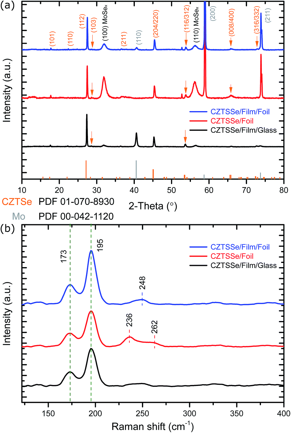 | ||
| Fig. 1 (a) XRD patterns and (b) Raman scattering spectra of absorber samples on different substrates. | ||
The texture coefficients (Chkl) and preferred orientation were calculated as described in ESI (S2†).17 As shown in Table S1 and Fig. S4,† the Chkl values increase for minor reflections (101), (211) and (400) for film deposited directly on Mo foil. While this would indicate a small randomisation of the sample texturing compared to film/foil and film/glass substrate, the absence of reflections at (110) and (332) points toward a slight preferred orientation (increase in σ value) along the minor planes.
In addition to the CZTSSe reflections, the Mo film on glass substrate shows mainly the (110) orientation while the bare Mo foil shows both the (200) and (211) orientations. Sputtered Mo on Mo foil shows all three diffraction planes (Fig. S5†). Despite these different orientations, Mo(S,Se)x is found on all three substrates at 31.9° and 56.3° corresponding to (100) and (110) planes following selenisation.18 In this case the Mo(S,Se)x grains are oriented perpendicular to the Mo substrate increasing the adhesion and the electrical conductivity19 but also facilitating the diffusion of Se, leading to a thicker Mo(S,Se)x layer.20 Interestingly, the strength of the Mo(S,Se)x peaks of samples on foil with sputtered Mo are weaker than those on bare foil. This suggests that the sputtered Mo has limited the formation of Mo(S,Se)x on this substrate.
The XRD results alone cannot conclusively confirm the crystal structure because of the peak positions for kesterite and stannite CZTSSe are the same as well as secondary phases such as ZnSe and Cu2SnSe3.21,22 Therefore, Raman spectroscopy was performed and, as shown in Fig. 1b, there is a dominant A1 symmetry mode of CZTSSe at 173 cm−1 and 195 cm−1.23 The presence of Raman peaks in the region of 236–248 cm−1 for the films on flexible foils can correspond to a mix mode of B/E24 modes.
Morphology and composition
Fig. 2 shows representative morphology of the samples on each substrate. For the reference sample on SLG, shown in Fig. 2a, the CZTSSe film has compact and rounded grains with a size of 1–2 μm forming a dense thin film. For the CZTSSe films on Mo foil shown in Fig. 2b and c, the grains are smaller with a size of 0.8–1.2 μm. This reduction in grain size is likely to stem from the absence of Na doping which is introduced by the SLG substrate. All three cross-sectional images (Fig. 2d–f) exhibit a characteristic bi-layer morphology associated the CZTS nanoparticle ink fabrication approach, i.e. a large grain layer on top of a fine-grain (FG) layer located between the CZTSSe layer and Mo back contact. The thickness of the large-grain (LG) CZTSSe layer was similar for all of the samples at around 750 nm. This is reasonable given that the same selenisation conditions were applied (selenium mass, temperature and time). We have previously reported that the selenisation process is controlled by metal cation re-ordering and grain boundary migration.25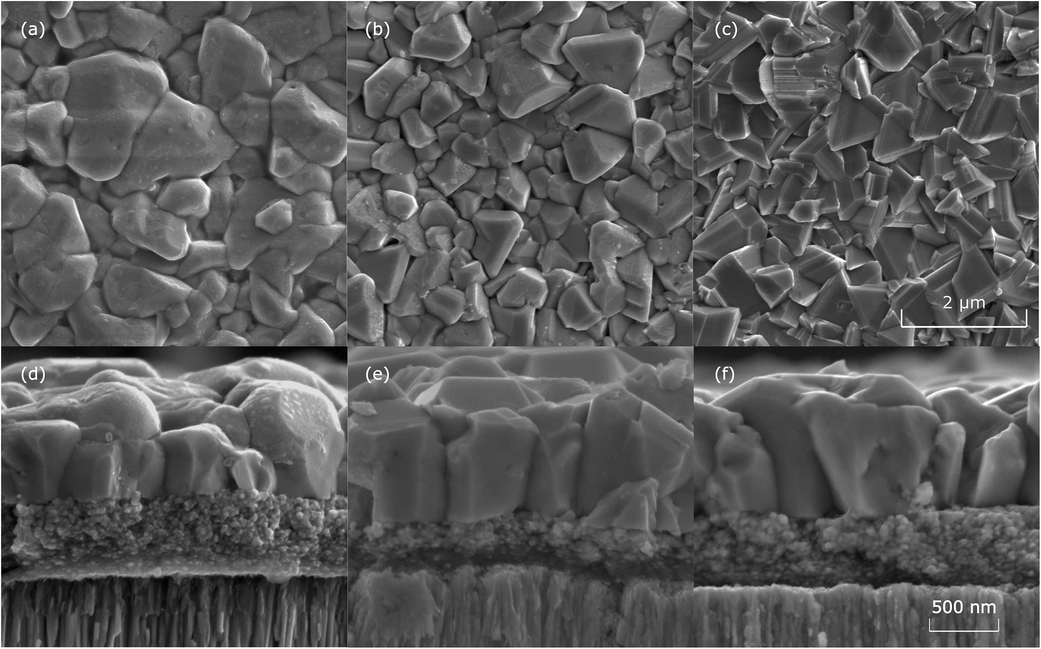 | ||
| Fig. 2 Surface morphology of CZTSSe sample on (a) SLG, (b) molybdenum foil and (c) molybdenum foil with Mo film. Cross-sectional image of samples on (d) SLG, (e) molybdenum foil and (f) molybdenum foil with Mo film. | ||
As shown in Fig. 3a, the full range cross-sectional image of CZTSSe on SLG, a thin 250 nm Mo(S,Se)x layer is formed between the CZTSSe absorber and Mo back contact during selenisation. This is similar for widely reported CZTSSe solar cells.26,27 On the other hand, for samples on Mo foil substrates (Fig. 3b and c), the Mo(S,Se)x layer was much thicker than that on SLG. This is especially true for the Mo(S,Se)x layer on bare Mo foil which was up to 7.2 μm. The application of a sputtered Mo film on Mo foil substrate reduced this to 2.4 μm. This difference between the samples is consistent with the trend observed in the XRD spectra for Mo(S,Se)x. The thicknesses of the Mo(S,Se)x layers were further confirmed with EDS line scans (Fig. 3d–f) corresponding to the red regions marked in Fig. 3a–c. It can be seen clearly from Fig. 3e and f that the layer between the flexible foil back contact and CZTSSe absorber consists mainly of Mo and Se in the atomic ratio of around 1![[thin space (1/6-em)]](https://www.rsc.org/images/entities/char_2009.gif) :2. For the sample on SLG (Fig. 3a), the Mo(S,Se)x formed only a thin layer on top of Mo film back contact.
:2. For the sample on SLG (Fig. 3a), the Mo(S,Se)x formed only a thin layer on top of Mo film back contact.
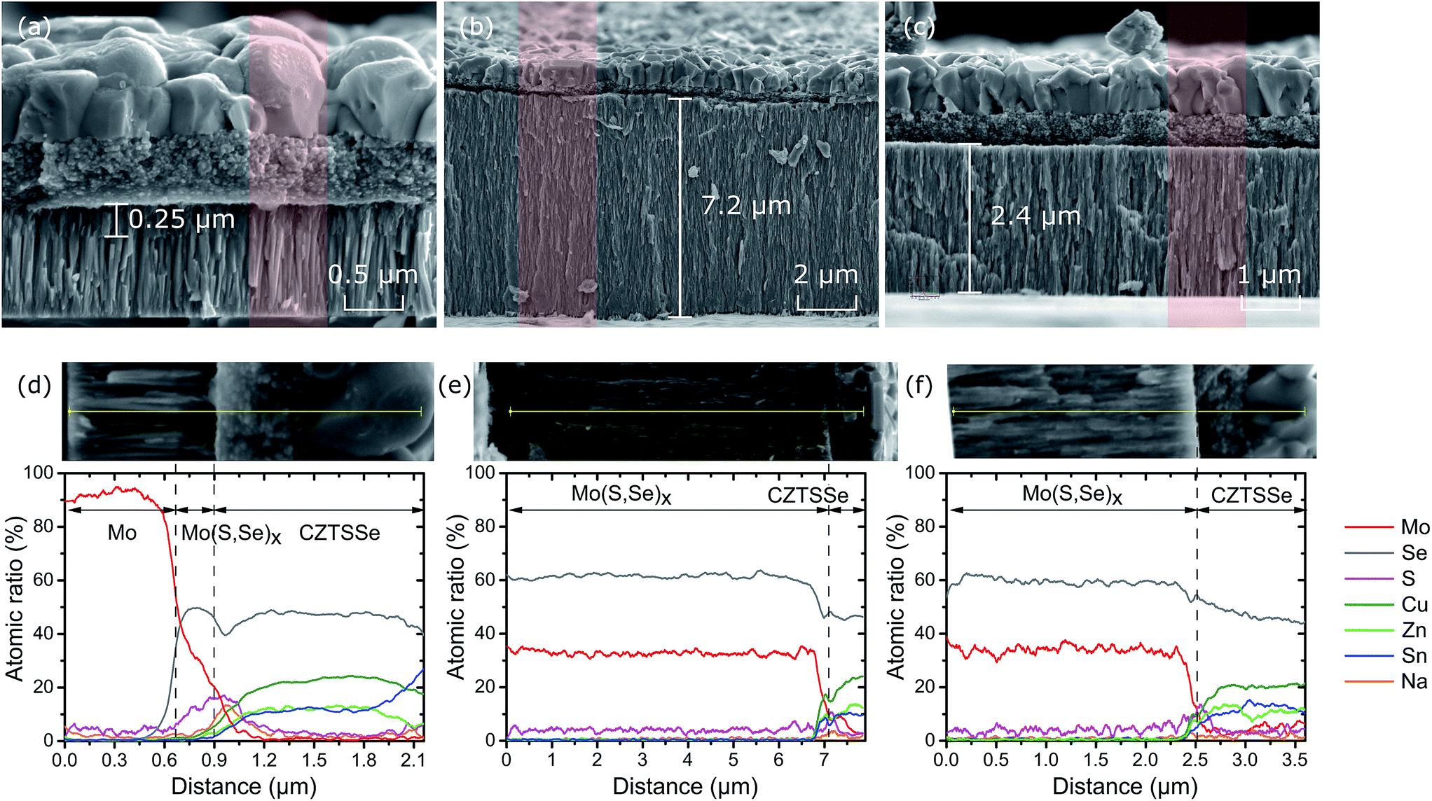 | ||
| Fig. 3 The full range cross-sectional SEM images for samples on (a) SLG, (b) molybdenum foil and (c) molybdenum foil with Mo film layer, and EDS line scans across the film thickness in (d), (e) and (f), respectively. The red regions show the positions of EDS line scans. | ||
Photovoltaic current–voltage characteristics
Thin film solar cells were fabricated on all three substrates and the current density (J) versus voltage (V) characteristics for champion devices are shown in Fig. 4a. The extracted photovoltaic performance characteristics together with average performance values are listed in Table 1. It can be seen that the device on SLG exhibited a power conversion efficiency (PCE) of 4.0% while in contrast the device on bare flexible Mo had a PCE of 1.5%. Despite achieving a similar VOC, the degradation can be attributed to a substantially increased series resistance Rs caused by the existence of the thick Mo(S,Se)x layer. The effect of the sputtered Mo layer is immediately clear in Fig. 4a as the PCE becomes comparable to the SLG device at 3.8%. Notably, the power density achieved with the flexible cell is more than double that of the device on SLG. From Table 1, it can be seen that while the flexible device achieves a similar value of Rs using a sputtered Mo layer, Rsh is significantly lower than the device on SLG. This is attributed to the increased grain boundary density in the CZTSSe absorber on foil substrates. For the Mo foil with sputtered Mo film device presented in Fig. 4a and Table 1, the thickness of the sputtered Mo layer was approximately 800 nm. Increasing this to 1200 nm further reduced this to 2.6 Ω cm2, confirming the hypothesis that limiting the formation of the Mo(S,Se)x layer reduces series resistance.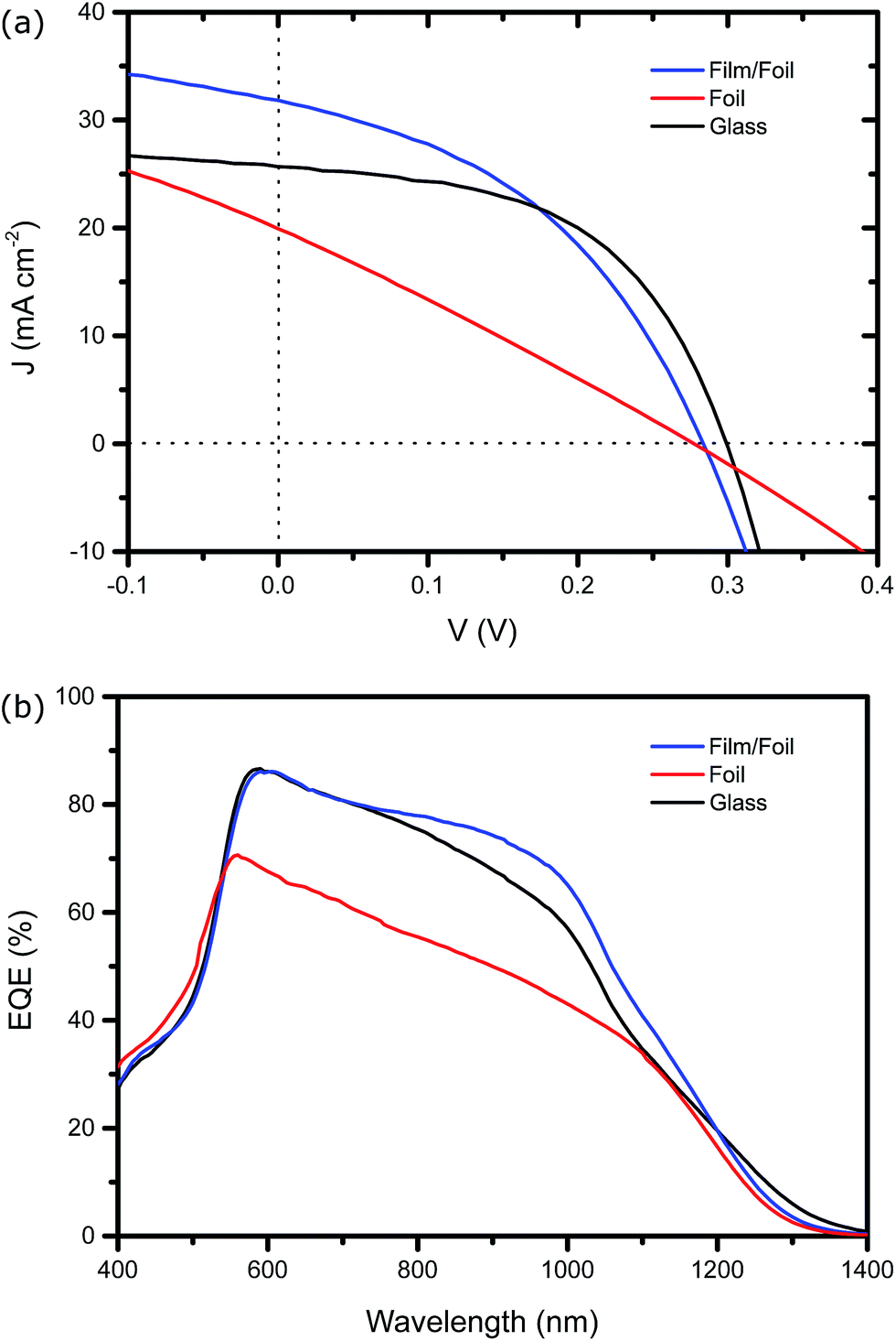 | ||
| Fig. 4 (a) JV curves and (b) EQE response of solar cells on rigid and flexible substrates. | ||
| Substrate | VOC (mV) | JSC (mA cm−2) | FF (%) | PCE (%) | Rs (Ω cm2) | Rsh (Ω cm2) |
|---|---|---|---|---|---|---|
| Mo foil | 280 (247 ± 7.0) | 19.9 (19.6 ± 1.9) | 27.3 (27.8 ± 0.4) | 1.5 (1.35 ± 0.17) | 12.2 | 16.7 |
| Mo foil + film | 280 (276 ± 9.6) | 31.8 (28.4 ± 3.8) | 42.6 (45.0 ± 2.4) | 3.8 (3.48 ± 0.24) | 2.9 | 36.3 |
| Glass | 300 (302 ± 7.8) | 25.7 (25.6 ± 0.8) | 53.8 (49.5 ± 2.4) | 4.0 (3.8 ± 0.19) | 2.5 | 72.8 |
Fig. 4b shows the EQE characteristics for the three devices. The signal for the device on bare foil is substantially reduced relative to the SLG and foil with sputtered Mo substrates. This is due to the vastly reduced collection probability created by a performance limiting Mo(S,Se)x layer. Interestingly, the EQE for the device on foil with sputtered Mo has a slightly larger EQE towards long wavelengths despite having smaller average grain size. This is consistent with the values of JSC obtained from Fig. 4a (and listed in Table 1) and suggests considerable potential for the technology.
Investigation of substrate impurities
In order to assess the quality of the Mo foil substrate onto which the CZTS nanoparticle inks were deposited, SIMS measurements were performed on the bare Mo foil and the Mo foil with a sputtered thin Mo film. These data are shown in Fig. 5, the bare foil substrate exhibits one and two orders of magnitude higher levels of Fe and Cr respectively, than the Mo foil with Mo film. Note that in the case of the Mo foil coated with Mo film, the ion beam has not penetrated through the sputtered Mo layer to the foil. As expected therefore, the sputtered Mo provides a purer substrate than the bare foil and may result in a better interface within the device. It can be concluded that on its own Mo foil is unsuitable as a substrate for flexible CZTSSe solar cells.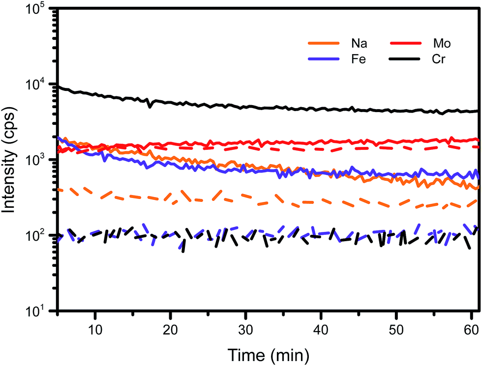 | ||
| Fig. 5 SIMS elemental depth profiles of Mo foil substrate (solid lines) and Mo foil coated with Mo film substrate (dash lines). | ||
Fig. 5 also indicates a difference in Na signal between the substrates which, although not as large as for Fe and Cr, is still significant. The influence of sodium incorporation on CZTSSe morphology and cell performances have been widely reported8,9,28–31 and it plays a positive role in the reduction of grain boundary density via the formation of large grains. The use of SLG as a rigid substrate in our work provides an intentional source of intrinsic Na doping. However, using Mo foil as a substrate unintentionally introduces Na into our process.
In addition to the Mo foil, background sources of Na may also exist in the process arising for example from the selenisation furnace.20 In order to assess the possible influence of these, elemental depth profiling was performed on devices built on all three substrates using SIMS as shown in Fig. 6. The SIMS data allow for identification of the various layers in the devices including the Mo(S,Se)x and FG/LG CZTSSe layers. All three samples exhibit an oscillating Na signal throughout the device which confirms the presence of uncontrolled Na sodium sources in the fabrication process. Interestingly, the device on SLG shows a local maximum in the Na signal in the FG CZTSSe layer (Fig. 6a) while in contrast the devices on foil show a local minima in the same region. This reduction may be responsible for the smaller average grain size observed in the LG CZTSSe layer in the foil devices and overall, these features merit further investigation to achieve comparable Rsh in Mo foil devices.
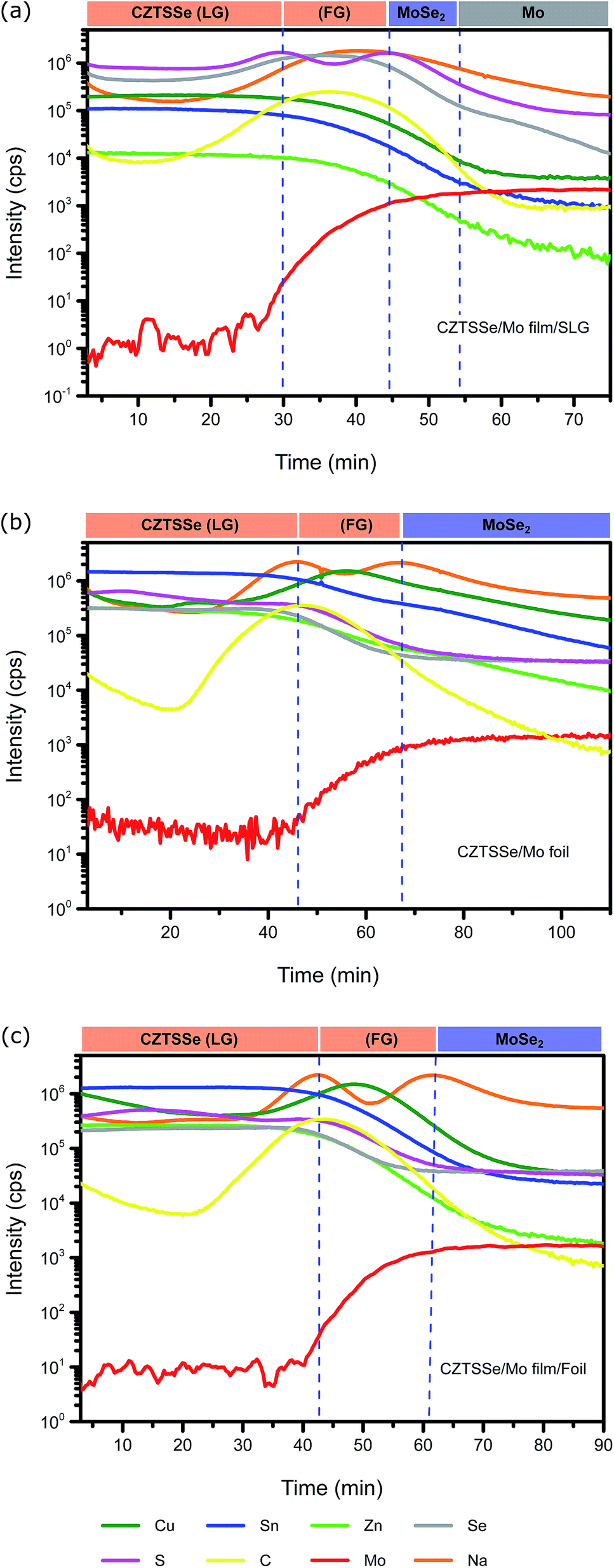 | ||
| Fig. 6 SIMS elemental depth profiles of CZTSSe on substrate (a) SLG, (b) molybdenum foil, and (c) molybdenum foil with Mo film layer. LG: larger-grain, FG: fine-grain. | ||
Conclusions
The performance of thin film CZTSSe solar cells fabricated on Mo foil substrates has been presented. It is found that on its own, Mo foil is an unsuitable substrate due to the formation of a thick Mo(S,Se)x layer formed during the fabrication. These effects can be mitigated by the introduction of a thin Mo sputtered layer which preserves the advantages of a low cost foil substrate that is compatible with high volume manufacturing. Devices on SLG contain an intrinsic source of Na doping which promotes the formation of large grains in the CZTSSe photovoltaic absorber. For development of the technology on foil substrates, it is necessary to develop approaches towards controlled introduction of Na, also achieve comparable grain sizes and Rsh to SLG.Conflicts of interest
There are no conflicts to declare.Acknowledgements
The authors gratefully acknowledge financial support for this work from the Engineering and Physical Sciences Research Council via grants: the North East Centre for Energy Materials (EP/N024389/1) and EP/R021503/1. We would also like to acknowledge useful interactions with Patrick Chapon (Horiba) and Kate Nicholson (Northumbria University).References
- X. Liu, Y. Feng, H. Cui, F. Liu, X. Hao, G. Conibeer, D. B. Mitzi and M. Green, Prog. Photovoltaics, 2016, 24, 879–898 Search PubMed.
- F. Luckert, D. I. Hamilton, M. V. Yakushev, N. S. Beattie, G. Zoppi, M. Moynihan, I. Forbes, A. V. Karotki, A. V. Mudryi, M. Grossberg, J. Krustok and R. W. Martin, Appl. Phys. Lett., 2011, 99, 062104 CrossRef.
- S. Yoshida, Solar Frontier Achieves World Record Thin-Film Solar Cell Efficiency of 22.9%, 2017, http://www.solar-frontier.com/eng/news/2017/<?pdb_no 1220?>1220<?pdb END?>_press.html Search PubMed.
- H. Zhou, W.-C. Hsu, H.-S. Duan, B. Bob, W. Yang, T.-B. Song, C.-J. Hsu and Y. Yang, Energy Environ. Sci., 2013, 6, 2822–2838 CAS.
- N. G. Dhere, Sol. Energy Mater. Sol. Cells, 2007, 91, 1376–1382 CrossRef CAS.
- W. Wang, M. T. Winkler, O. Gunawan, T. Gokmen, T. K. Todorov, Y. Zhu and D. B. Mitzi, Adv. Energy Mater., 2014, 4, 1301465 CrossRef.
- C. J. Hages, M. J. Koeper, C. K. Miskin, K. W. Brew and R. Agrawal, Chem. Mater., 2016, 28, 7703–7714 CrossRef CAS.
- S. Lopez-Marino, Y. Sanchez, M. Espindola-Rodriguez, X. Alcobe, H. Xie, M. Neuschitzer, I. Becerril, S. Giraldo, M. Dimitrievska, M. Placidi, L. Fourdrinier, V. Izquierdo-Roca, A. Perez-Rodriguez and E. Saucedo, J. Mater. Chem. A, 2016, 4, 1895–1907 CAS.
- K. Sun, F. Liu, C. Yan, F. Zhou, J. Huang, Y. Shen, R. Liu and X. Hao, Sol. Energy Mater. Sol. Cells, 2016, 157, 565–571 CrossRef CAS.
- K. W. Brew, S. M. McLeod, S. M. Garner and R. Agrawal, Thin Solid Films, 2017, 642, 110–116 CrossRef CAS.
- P. Reinhard, A. Chirilă, P. Blösch, F. Pianezzi, S. Nishiwaki, S. Buecheler and A. N. Tiwari, IEEE J. Photovolt., 2013, 3, 572–580 CrossRef.
- Y. Zhang, Q. Ye, J. Liu, H. Chen, X. He, C. Liao, J. Han, H. Wang, J. Mei and W. Lau, RSC Adv., 2014, 4, 23666–23669 RSC.
- P. Hidnert, W. B. Gero and S. United, Thermal expansion of molybdenum, U.S. Dept. of Commerce, Bureau of Standards: U.S. Govt. Print. Off., Washington, D.C., 1924, vol. 19, pp. 429–444 Search PubMed.
- Y. Qu, G. Zoppi, R. W. Miles and N. S. Beattie, Mater. Res. Express, 2014, 1, 045040 CrossRef.
- M. A. Baker, Thin Solid Films, 1980, 69, 359–368 CrossRef CAS.
- S. C. Riha, B. A. Parkinson and A. L. Prieto, J. Am. Chem. Soc., 2011, 133, 15272–15275 CrossRef CAS PubMed.
- G. Zoppi, K. Durose, S. Irvine and V. Barrioz, Semicond. Sci. Technol., 2006, 21, 763 CrossRef CAS.
- P. B. James and M. T. Lavik, Acta Crystallogr., 1963, 16, 1183 CrossRef CAS.
- R. Würz, D. Fuertes Marrón, A. Meeder, A. Rumberg, S. M. Babu, T. Schedel-Niedrig, U. Bloeck, P. Schubert-Bischoff and M. C. Lux-Steiner, Thin Solid Films, 2003, 431, 398–402 CrossRef.
- D. Abou-Ras, D. Mukherji, G. Kostorz, D. Brémaud, M. Kälin, D. Rudmann, M. Döbeli and A. N. Tiwari, MRS Online Proc. Libr., 2005, 865, 1946–4274 Search PubMed.
- B. Ananthoju, J. Mohapatra, M. K. Jangid, D. Bahadur, N. V. Medhekar and M. Aslam, Sci. Rep., 2016, 6, 35369 CrossRef CAS PubMed.
- P. A. Fernandes, P. M. P. Salomé and A. F. da Cunha, J. Alloys Compd., 2011, 509, 7600–7606 CrossRef CAS.
- P. M. P. Salomé, P. A. Fernandes and A. F. da Cunha, Thin Solid Films, 2009, 517, 2531–2534 CrossRef.
- M. A. Hossain, M. Wang and K.-L. Choy, ACS Appl. Mater. Interfaces, 2015, 7, 22497–22503 CAS.
- Y. Qu, G. Zoppi and N. S. Beattie, Sol. Energy Mater. Sol. Cells, 2016, 158, 130–137 CrossRef CAS.
- C. K. Miskin, W.-C. Yang, C. J. Hages, N. J. Carter, C. S. Joglekar, E. A. Stach and R. Agrawal, Prog. Photovoltaics, 2015, 23, 654–659 CAS.
- Y. Qu, G. Zoppi and N. S. Beattie, Prog. Photovoltaics, 2016, 24, 836–845 CAS.
- D. Colombara, U. Berner, A. Ciccioli, J. C. Malaquias, T. Bertram, A. Crossay, M. Schöneich, H. J. Meadows, D. Regesch, S. Delsante, G. Gigli, N. Valle, J. Guillot, B. El Adib, P. Grysan and P. J. Dale, Sci. Rep., 2017, 7, 43266 CrossRef PubMed.
- H. A. Al-Thani, F. S. Hasoon, M. Young, S. Asher, J. L. Alleman, M. M. Al-Jassim and D. L. Williamson, 29th IEEE PVSC, Research Org., National Renewable Energy Lab., Golden, CO, US, 2002 Search PubMed.
- J. V. Li, D. Kuciauskas, M. R. Young and I. L. Repins, Appl. Phys. Lett., 2013, 102, 163905 CrossRef.
- H. Zhou, T.-B. Song, W.-C. Hsu, S. Luo, S. Ye, H.-S. Duan, C.-J. Hsu, W. Yang and Y. Yang, J. Am. Chem. Soc., 2013, 135, 15998–16001 CrossRef CAS PubMed.
Footnote |
| † Electronic supplementary information (ESI) available. See DOI: 10.1039/c7ra13336g |
| This journal is © The Royal Society of Chemistry 2018 |