
 Open Access Article
 This Open Access Article is licensed under a Creative Commons Attribution-Non Commercial 3.0 Unported Licence
Defect-concentration dependence of electrical transport mechanisms in CuO nanowires†
Zufang Lina,
Runze Zhana,
Luying Lib,
Huihui Liuc,
Shuangfeng Jiac,
Huanjun Chena,
Shuai Tang a,
Juncong Shea,
Shaozhi Denga,
Ningsheng Xua and
Jun Chen*a
a,
Juncong Shea,
Shaozhi Denga,
Ningsheng Xua and
Jun Chen*a
aState Key Laboratory of Optoelectronic Materials and Technologies, Provincial Key Laboratory of Display Material and Technology, School of Electronics and Information Technology, Sun Yat-sen University, School of Physics and Engineering, Guangzhou, 510275 China. E-mail: stscjun@mail.sysu.edu.cn
bWuhan National Laboratory for Optoelectronics, Huazhong University of Science and Technology, Wuhan, 430074 China
cSchool of Physics and Technology, Center for Electron Microscopy, Wuhan University, Wuhan, 430072 China
First published on 9th January 2018
Abstract
Investigations of the transport mechanisms of individual nanowires are important for advancing their use in applications. Based on statistical results for the temperature-dependent electrical characteristics of individual CuO nanowires, and by characterizing them using transmission electron microscopy, we have found that the defect concentration is the most important parameter affecting electron transport in nanowires. Space-charge-limited currents can be observed for sufficiently high applied voltages, for example about 10 V. In the ohmic regime, before the current–voltage curves of nanowires enter the trap-filling stage, three main transport mechanisms have been proposed. They are related to the defect concentrations and include combinations of defect-induced nearest-neighbor hopping, trap activation, and intrinsic excitation. Numerical calculations using the model to fit the experimental data agree very well, confirming the proposed transport mechanisms.
Introduction
One-dimensional (1D) semiconductor nanostructures have attracted the attention of numerous scientists over the past two decades because of their unique electronic, optical, photoelectrochemical, and mechanical properties1–6 and due to their important prospects for applications in nanoelectronic devices.7–10 However, there are still many problems to be solved, such as how to improve the electrical uniformity of nanowire electronic devices. The electrical transport mechanisms of nanowires are critical for resolving these problems. It is also very important to understand the special characteristics of nanowires for targeted applications in nanoelectronic devices.Much effort has been devoted to studies of the transport properties of oxide semiconductor nanowires.11–16 Various transport mechanisms have been proposed to explain the experimental results, but no unified mechanism exists, even for the same kinds of nanowires. Proposed transport mechanisms include defect-induced thermal activation, variable-range hopping, nearest-neighbor hopping (NNH), and space-charge-limited currents (SCLC).11,12,17–21 Further, most of these studies have focused on n-type nanowires, with only a few dealing with p-type nanowires, which enable complementary devices.
Cupric oxide (CuO) is a representative natural p-type semiconductor, and CuO nanowires can be synthesized on copper substrates via thermal oxidation.22 Such nanowires have attracted much attention for applications in memristors, in heterojunctions, as electrodes for lithium-ion and lithium–air batteries, and in sensors.23–29 Understanding the electrical transport mechanisms in CuO nanowires is essential for realizing their applications in devices and for improving their performance. Until now, very little work has been carried out on this topic. Based on their temperature-dependent current–voltage (I–V) characteristics, Wu et al. proposed that thermal activation, phonon scattering, and polaron hopping may all contribute to the transport process, depending on the applied voltage and temperature.21 Florica et al. discovered that NNH dominates at low temperatures, compared with thermal activation at high temperatures.19 The results of these two studies differ significantly from each other, and statistically significant results are lacking. Thus, more detailed studies of the transport mechanisms are needed to discover the reasons for these differences and to pinpoint the factors that determine the actual transport mechanisms.
In the present work, we used CuO nanowires to look for insights into the transport mechanisms of p-type semiconductor nanowires. By analyzing statistical results for the temperature-dependent electrical characteristics of individual CuO nanowires, and by characterizing them using transmission electron microscopy (TEM), we have identified three types of mechanisms, which depend upon the defect concentrations. The results provide a guide for improving the properties of electronic devices. Specifically, to improve the uniformity of nanowire electronic devices, our results show that it will be necessary to employ nanowires with a small range of defect concentrations. Furthermore, we can choose nanowires with specific defect concentrations for special applications.
Experiment
CuO nanowires were synthesized using thermal oxidation method.21,22 In brief, Cu foils (5 mm × 8 mm, Alfa Aesar, 99.998%) were etched by an aqueous HCl solution (10%) to remove the contaminations and native oxide. Then the foils were cleaned in acetone, alcohol and deionized water under ultrasonic bath for 15 min, respectively. After dried by the nitrogen gas flow, the foils were loaded in a quartz plate and placed in the center of a muffle furnace. The heating rate was ∼2 °C min−1 and the oxidation temperature was 450 °C. The foils were oxidized in air isothermally at 450 °C for 360 min. After oxidation, they were cooled down to room temperature naturally. We employed scanning electron microscopy (SEM, Zeiss SUPER-60), X-ray diffraction (XRD), and transmission electron microscopy (TEM, Titan™ G2 60-300) to characterize the prepared nanowires.To measure the electrical transport properties of a single CuO nanowire, we used a two-electrode configuration fabricated using UV (ultraviolet) photolithography. In brief, the CuO nanowires were first dispersed in alcohol and were then transferred to a quartz-glass substrate by spin-casting. We employed a lift-off process using UV photolithography to form the electrodes. Ni or Au films approximately 200 nm thick were deposited on the dispersed CuO nanowires by magnetron sputtering. Both the widths of the electrodes and the gap between the two electrodes were approximately 2 μm. We chose Ni as the main electrode material because the work functions of Ni (Φ = 4.99 eV) and CuO (Φ = 4.78 eV (ref. 30)) enable ohmic contact to be obtained. Moreover, the adhesion property of the Ni electrode is excellent, and the lift-off process is easy to carry out. Furthermore, the oxidation layer at the surface of the electrode has a negligible influence on the results, as we confirmed by electrical measurements and X-ray photoelectron spectroscopy (see ESI Fig. S1 and S2† online) of the Ni electrodes. In our experiments, the electrical properties of the samples that use Ni as the electrode were repeatable and stable even after the samples were kept for several months. We note that Au or Pt are usually employed as contact electrodes for measurements of such nanostructures, and we also used Au as the electrodes for some samples. We found that the conductivities of the samples measured using Au electrodes have the same distribution as those obtained using Ni electrodes (see ESI Fig. S3† online), but the lift-off process when using Au as the electrode material is much more difficult.
We measured the I–V properties on a Cascade probe station using a semiconductor parameter analyzer (Agilent Technologies B1500A). We swept the applied voltage from −10 to 10 V, in steps of 0.1 or 0.02 V. Before each test, we annealed the samples to be measured at 413 K for 240 min in order to minimize the effects of gaseous absorption on the surfaces. All of the I–V curves were measured in thermal equilibrium. They were measured at different temperatures by varying the temperature of the sample stage from 213 to 393 K (except for three samples that were varied from 293 K to 353 K). The samples were immersed in a nitrogen atmosphere during the measurements, and all of the measurements were carried out in the dark.
Results and discussion
Morphology and structure
The top-view SEM image in Fig. 1(a) shows the morphology of the as-grown CuO nanowires; a magnified image of one of the nanowires is presented in the inset. The prepared nanowires are approximately 2–20 μm in length and 30–300 nm in diameter. Fig. 1(b) shows a cross-sectional SEM image and (c) shows an XRD measurement of the CuO nanowires grown on the Cu substrate. The Cu2O phase that appears in the XRD data is from an interlayer between the CuO nanowires and Cu substrate.31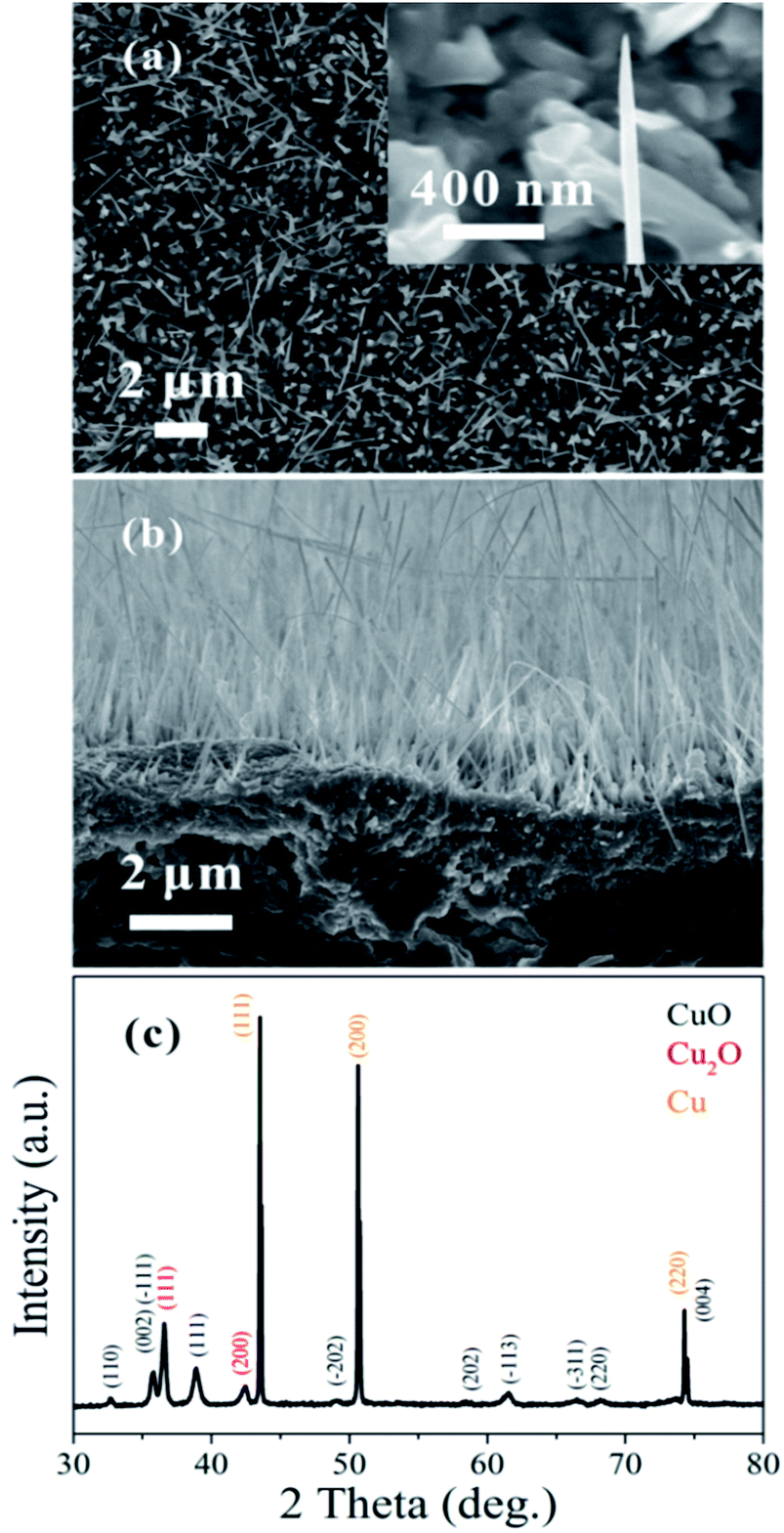 | ||
| Fig. 1 (a) Top-view SEM image of the prepared CuO nanowires; the inset shows a magnified SEM image. (b) Cross-sectional SEM image. (c) XRD measurement of the CuO nanowires. | ||
I–V characteristics of CuO nanowires at room temperature (RT)
A representative SEM image of the fabricated structure is shown in the upper right inset of Fig. 2(a). Approximately 200 single nanowires were measured, and most of the samples exhibited similar symmetric and nonlinear behaviors [see the bottom-right insets of Fig. 2(b) and (c)] over a voltage range of −10 to 10 V. Several conduction mechanisms are commonly used to explain the transport properties of materials, and the relationship between I and V differs for each mechanism. We can therefore use those characteristics to distinguish among the various transport mechanisms. From fitting to the measurements, we can easily exclude Fowler–Nordheim tunneling, direct tunneling, thermionic field emission, and the Poole–Frenkel emission mechanisms.32 Symmetric I–V characteristics are expected from an ideal back-to-back Schottky diode configuration. However, we can exclude this mechanism because the back-to-back Schottky model21 does not fit our data (see ESI Fig. S4†).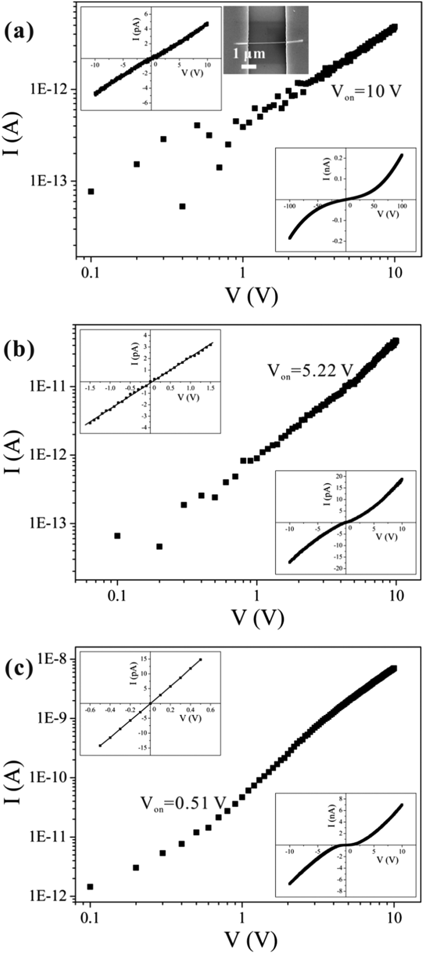 | ||
| Fig. 2 Three representative I–V characteristics are shown here. (a) Type I: the I–V curve is linear between 0 and 10 V. The inset at the upper left shows the I–V curve for −10 to 10 V, and the upper right shows an SEM image of the measurement structure. The I–V curve for −100 to 100 V—for which the applied voltage exceeds Von (see text)—is given at the bottom right. (b) Type II: the I–V curves deviate from linearity between 0 and 10 V. The inset at the upper left shows the I–V curve for −1.5 to 1.5 V, when the applied voltage does not exceed Von, and the bottom right shows the I–V curve for −10 to 10 V. (c) Type III: the I–V curve shows three distinct regimes in the voltage range of 0 to 10 V. The inset at the upper left shows the I–V curve between −0.5 and 0.5 V, at low voltages that do not exceed Von; the bottom right shows the I–V curve between −10 and 10 V. | ||
According to the I–V curves, the experimental results can be divided into three categories, as shown in Fig. 2, which we refer to as type I, type II, and type III; there were, respectively, 47, 121, and 41 samples of each type. We believe that the conduction mechanism in these nanowires is SCLC. For low applied voltages that do not exceed Von (the threshold voltage, at which the number of injected carriers exceeds that of thermally generated carriers), the conduction is ohmic, as can be seen in the insets in the upper-left corners of Fig. 2(a)–(c). Hereafter, we refer to this low-voltage region as the “ohmic-conduction region”. If the applied voltage exceeds Von, then the I–V curves become nonlinear, and conduction shifts from ohmic conduction to a trap-filling process. This is indicated by the symmetric, nonlinear characteristics that appear in the I–V curves [as shown in the insets in the bottom-right corners of Fig. 2(a)–(c)]. The transport mechanisms have different values of Von for the three categories of nanowires, as shown in Fig. 2(a)–(c); the value of Von for type I is the largest (10 V), while type III has the smallest value (0.51 V).
The different conductivities are not caused by different diameters or contacted lengths of the nanowires (see ESI Fig. S5†). We propose that the differences in the defect concentrations are the cause of the different conductivities of nanowires synthesized under the same conditions. Defects are expected to exist widely in nanomaterials,33 and different defect concentrations may relate to different growth mechanisms. As reported in the literature, a stress-induced growth mechanism occurs for CuO nanowires prepared by thermal oxidation.31,34–36 Stress accumulates during oxidation of the thin copper film. It is possible that the stress-nucleation sites may differ from each other due to differences in the stress distributions at a microscopic scale. Furthermore, in the process of growth, both stresses and oxygen transport may differ among the nanowires, which inevitably leads to differences in defect concentrations in the nanowires.
TEM characterization of nanowires with different conductivities
We chose several CuO nanowires (type I and type III samples) for TEM characterization, picking them out using a modified SEM system (Zeiss Supra 55). The system is equipped with two tungsten probes that can be precisely manipulated. In our experiment, one of the tungsten probes was moved to touch the bottom part of a nanowire, and a thin layer of carbon was deposited on the contact point. The probe was then pulled in a direction opposite to that of the substrate, separating the nanowire from the substrate. The tip of the nanowire was fixed on the second probe using the same procedure. Then we carried out our I–V property measurements, and we chose the nanowires according to their measured I–V properties.The morphology and structural characterizations of the nanowires are shown in Fig. 3. The images show that some nanoparticles are present on the surfaces of the nanowires. The diameters of all the nanoparticles are less than 10 nm, and the numbers of nanoparticles differ greatly between these two samples. Fig. 3(a) shows a low-resolution TEM image, a selected-area electron-diffraction pattern (SAED), and a high-resolution TEM image of a type I sample, for which the conductivity is the lowest. The good crystalline nature of the nanowire can be seen from the TEM image, except a few nanoparticles. Some of the nanoparticles are outlined by white circles in the high-resolution TEM image, and the inset shows a magnified image of one the nanoparticles. The SAED pattern also indicates the excellent crystal structure of the nanowire. Fig. 3(b) shows the corresponding micrographs for a type III sample, for which the conductivity is the highest. Note that the TEM image of the type III sample is blurry, in contrast to the corresponding type I image. The uneven distribution and rough surface can be seen in the low-resolution TEM image, and the structure of the nanowire is a bit difficult to distinguish in the high-resolution micrograph. Many nanoparticles can be seen on the sample surface. The SAED pattern shows the good crystal quality of the nanowire, with extra diffraction spots caused by diffraction from the nanoparticles (see the simulation results of the SAED pattern in ESI Fig. S5†). The zone axis of the diffraction spots indicated by the red arrows is different with the white ones and the blue lines show the ring patterns. Some of the nanoparticles have been outlined by white circles, and the inset shows a magnified image of one the nanoparticles. In the SAED patterns from both samples, ring patterns can be seen faintly, which are ascribed to the existence of the nanoparticles.
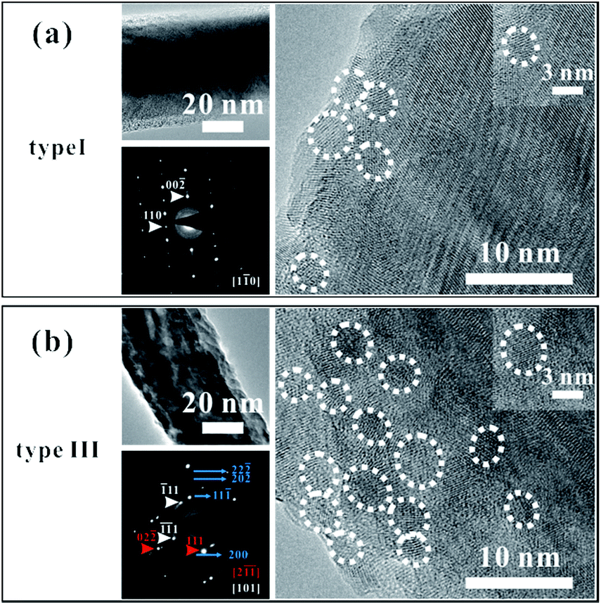 | ||
| Fig. 3 (a) Low-resolution TEM image (upper left), selected-area electron-diffraction (SAED) pattern; (bottom left), and high-resolution TEM image (right) for a type I sample. The inset shows a magnified image of one the nanoparticles. (b) Low-resolution TEM image (upper left), SAED (bottom left, which has contributions from both [101] and [2-1-1] axes, the existing diffraction rings can be attributed to the arbitrary orientations of CuO nanoparticles), and high-resolution TEM image (right) for a type III sample. The inset shows a magnified image of one the nanoparticles. | ||
We attribute the different defect concentrations in the different nanowires to the existence of the nanoparticles. Copper vacancies are the main defects in CuO, as has been reported in previous work, with the defect states located at an energy about 300 meV above the valance band.37 Because of their small sizes and specific surface areas, the nanoparticles have much higher Cu vacancy concentrations than the bulk of the nanowire.33 Therefore, higher defect concentrations are expected for type III samples than for type I.
Temperature dependence of the I–V characteristics of individual CuO nanowires
We chose approximately 30 single nanowires that showed perfectly linear properties in the low-applied-voltage region for these measurements, and the current increased in all of them with increasing temperature. It is worth noting that there are two reasons why the contact resistance between the nanowire and electrode in the temperature-dependent I–V measurement may be negligible. First, CuO nanowires have intrinsically high resistance, so the contribution of the contact resistance is not very prominent. Second, the contact resistance does not change significantly with increasing temperature. Some reports have indeed pointed out that the influence of the contact resistance on the value of the activation energy is negligible.19Fig. 4 shows the three typical types of temperature-dependent I–V characteristics. According to the SCLC theory, the defect concentration can be determined using eqn (1),21,38,39
| NT = 2εVc/qL2 | (1) |
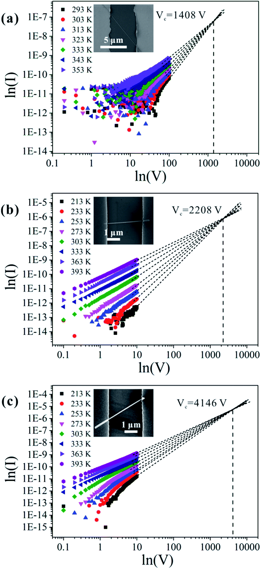 | ||
| Fig. 4 Measured I–V characteristics at different temperatures, and linear extrapolations of the I–V characteristics to obtain the crossover voltage.42 Panel (a) corresponds to type I results, (b) to type II results, and (c) to type III results. The current I is in ampere, and the voltage V is in volt. The insets show the corresponding SEM images of each nanowire. | ||
For the nanowires we studied in this work, ε is a constant; thus, the value of NT depends on Vc/L2. The lengths of the contacted nanowires presented in Fig. 4(a)–(c) are 8.029 μm, 2.626 μm, and 2.95 μm, respectively. The calculated values of the defect concentrations for each type in this study are 4.83 × 1016 cm−3, 7.01 × 1017 cm−3, and 1.06 × 1018 cm−3, respectively; therefore, the defect concentration is different for different nanowires. It is lowest in type I and highest in type III samples, which agrees well with the conclusion drawn in the preceding section.
Over the temperature range we investigated, if all of the nanowires were to undergo the same thermal activation process in the ohmic-conduction region (which reveals the native property of the nanowires), then we would expect type III samples to have the largest values of Von, because the carrier density increases with increasing NT.40,41 However, this conclusion disagrees with the experimental results we obtained in the RT measurements. The most probable reason for this is that the transport process in the ohmic-conduction region is not consistent in this temperature region. Defect concentrations can influence the critical temperature at which a semiconductor changes from one conductivity regime to another, and if the range of temperature variation remains unchanged, then nanowires with different defect concentrations may have different transport processes.
Discussion
To analyse the different transport processes in detail, we fitted our experimental conductivity data using an Arrhenius plot in the ohmic-conduction region. In an Arrhenius plot, the activation energy is a constant, and the conductivity is given by11
σ = σ0![[thin space (1/6-em)]](https://www.rsc.org/images/entities/char_2009.gif) exp(−Ea/kBT) exp(−Ea/kBT)
| (2) |
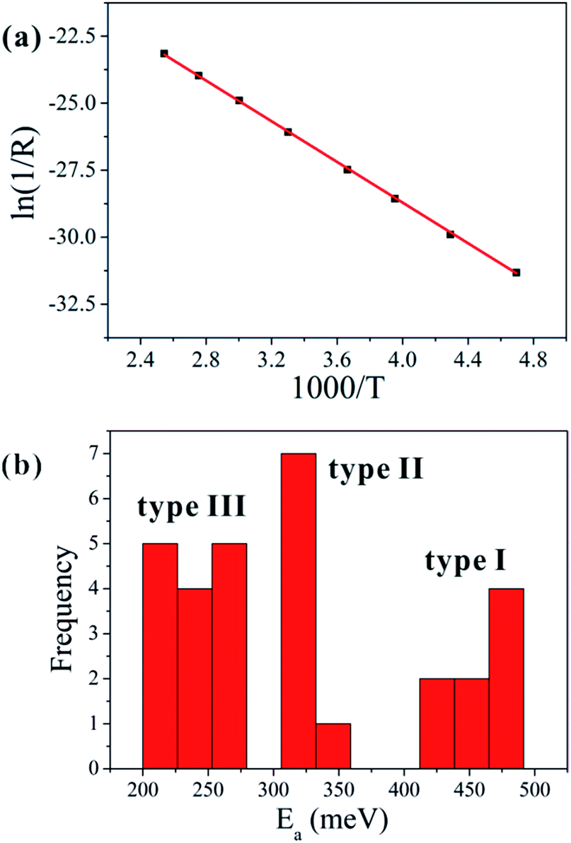
Fig. 5(a) shows a typical Arrhenius plot for one of our samples, which can be fitted well with a straight line. The activation energy can be determined from the slope of the Arrhenius plot.17,18 For example, the calculated value of the activation energy for the sample presented in Fig. 5(a) is approximately 327 meV, which is related to the central level of the defect.
 | ||
| Fig. 5 (a) Logarithm of the reciprocal resistivity as a function of reciprocal temperature (Arrhenius plot) for a single CuO nanowire sample. The resistivity R is in ohms, and the temperature is in K. (b) Frequency distribution of the activation energy. | ||
The frequency distribution of the activation energies for the samples we studied is shown in Fig. 5(b), which reveals three clusters of values centered near 240, 320, and 450 meV. The activation energy of the type I nanowires is the largest, and it is smallest for the type III nanowires. Furthermore, the activation energy of type II is similar to the reported defect level of Cu vacancies in the p-type conduction band of CuO, which is located at an energy 300 meV above the valance band.
As all the CuO nanowires were prepared under the same conditions, there should not be much variation in the defect type and defect energy levels. Therefore, the activation energy should be a fixed value related to the defect energy level, if thermal activation were the only transport mechanism. However, the calculated values of the activation energy are not fixed, which points to the existence of different transport processes in the ohmic-conduction region. As shown in Fig. 5(b), the activation energies are distributed in three clusters, which agree with the three types of nanowires categorized from the I–V curves.
We propose that electron transport in a nanowire is a mix of different transport mechanisms. It is known that two kinds of defect-related conduction mechanisms may be responsible for temperature-dependent conductivity, i.e., thermal activation and NNH, which obeys the Arrhenius relationship and shows I ∝ V at RT. Thus, the three transport types can be described as follows: trap activation mixed with intrinsic excitation (referred to as type I); trap activation only (referred to as type II); and NNH mixed with trap activation (referred to as type III).
As we have seen, the activation energy of the type I nanowires is the largest. It is close to the intrinsic Fermi level (0.6 eV) of the CuO nanowires (bandgap ∼1.2 eV).42 Therefore, intrinsic excitation can be assumed to be a component of the transport process for these nanowires. The number of surface nanoparticles for this kind of sample is the lowest, and consequently the defect concentration also is the lowest. Intrinsic excitation is more likely to occur at a low temperature. With the inclusion of intrinsic excitation, the carrier concentrations of the nanowires should increase dramatically at RT, which is likely to cause this type to have the largest Von. A schematic energy diagram for this process is represented in the inset at the upper left of Fig. 6, while the bottom left shows a schematic view of structure we measured. The conductance of the nanowires can be expressed as
|
G = G1 + G2 = G01exp(−Ea-trap/kBT) + G02exp(−Eg/2kBT)
| (3) |
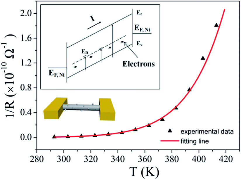 | ||
| Fig. 6 Plot of experimental data and fitted curve for the conductance using the type I transport model: trap activation mixed with intrinsic excitation. The inset at the upper left shows the schematic energy diagram for this transport process, while the bottom left shows a schematic view of structure measured. | ||
Fig. 6 shows the fitted result obtained using eqn (3) for the type I mechanism for one of the CuO nanowires. The values of the fitted parameters are as follows: G01 = 31.26 S, G02 = 5.2 × 10⁵ S, Ea-trap = 320 meV, and Eg = 1.2 eV.
As noted above, the activation energy for type II nanowires is approximately that of the Cu vacancy energy level (300 meV), which is in agreement with trap-activation theory. The conductance of the nanowire is described by
|
G = G0exp(−Ea-trap/kBT)
| (4) |
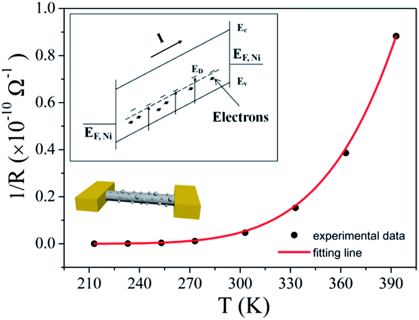 | ||
| Fig. 7 Experimental data and fitted curve for the conductance using the type II transport model: trap activation. The inset at the upper left shows the energy diagram, which represents the energy and the spatial distribution of defect states and illustrates the transport process. The inset at the bottom left is a schematic view of the structure measured. | ||
From the probability distribution shown in Fig. 5(b), we find that the defect energy level lies at approximately 320 meV above the valance band. For this case, the transport process is as illustrated in the inset of Fig. 7. When extra voltage is applied to the nanowire, the electric field along the nanowire increases. The presence of defects makes it easier for electrons in the nanoparticles to move forward, leaving a vacancy at the original position. These electrons are injected into the core of the nanowire for transport, and other electrons move in to occupy the vacancy. From the viewpoint of band theory, the electrons increasingly gain in energy with increasing temperature, and they are thus excited from the valance band to the defect energy level, leaving more vacancies in the valance band and promoting conductivity.
The calculated value of the activation energy for the type III samples is very low, i.e., approximately 225 meV, if the trap-activation model is applied. There are many nanoparticles on the surfaces of the type III nanowires, some of them in contact with each other. Electrons can transfer from one nanoparticle to another by hopping, which is similar to the transport process in multicrystalline or amorphous structures. Other electrons are injected into the core of the nanowire for transport, just as for type II. Due to the high defect concentration, type III nanowires require a higher temperature to transition from the NNH region to the trap-activation region. From the viewpoint of band theory, the activation process in this temperature range actually includes two processes: (i) NNH, in which electrons are ionized from an occupied state to the nearest empty state, producing vacancies for hopping,43 and (ii) trap activation, in which electrons transition from the valance band to the defect level, thereby supplying electrons to, and leaving holes in, the valance band, which promotes charge transport. In this case, the carrier concentration is determined by carriers generated both through NNH and through trap activation. At RT, the defects are weakly ionized, and NNH dominates, so the carrier concentration for this type is lower than for cases in which trap-activation dominates. Therefore, the smallest values of Von are obtained for nanowires of this type. With increasing temperature, the contribution of trap activation for this type of nanowire becomes more apparent. The conductance of the type III nanowires can be expressed as
|
G = G1 + G2 = G01exp(−Ea-NNH/kBT) + G02exp(−Ea-trap/kBT)
| (5) |
Fig. 8 shows the fitting plot of the conductance using NNH combined with the trap-activation model. The values of the fitted parameters are G01 = 9.34 × 10⁻⁵ S, G02 = 94.93 S, Ea-NNH = 30 meV, and Ea-trap = 320 meV. The insets in Fig. 8 show the schematic energy diagram for this mixed-transport process.
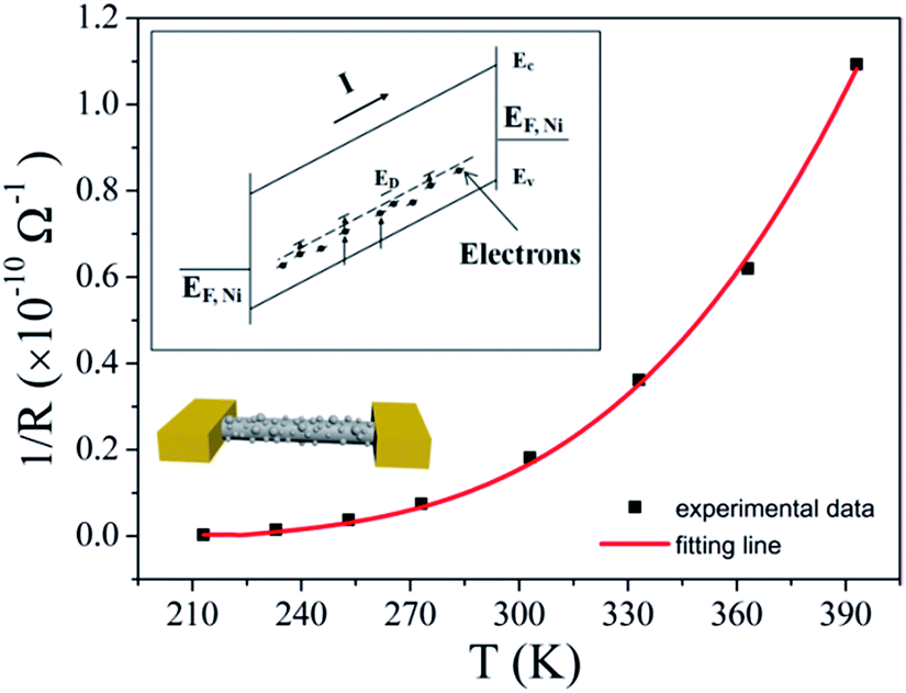 | ||
| Fig. 8 Fitting plot of the conductance using the type III transport model: NNH mixed with trap activation. The inset at the upper left shows the schematic energy diagram for this transport process, while the bottom left shows a schematic view of the structure measured. | ||
Conclusions
In summary, different defect concentrations induced three types of transport mechanisms in our CuO nanowires samples. In the temperature range 213–393 K, nanowires with activation energies of ∼320 meV exhibited type II transport processes. Those with large defect concentrations underwent a type III transport process, and intrinsic excitation may be involved for those with the fewest defects (type I).The numerical calculations further confirm these transport mechanisms. According to this theory, the defect concentration is an important parameter in semiconductor conduction, as it determines the dominant mechanism in the transport process. With well-established experimental facts, numerical calculations, and corresponding band-theory explanations, our work has increased the understanding of the transport mechanisms in CuO nanowires and provides a guide for improving the uniformity of electronic devices, which is important for applications of semiconducting nanowires in electronic devices.
Conflicts of interest
There are no conflicts to declare.Author contributions
J. C. planned the project. Z. L. carried out the measurement work, theoretical deduction and data analysis. R. Z. carried out the TEM characterization. S. T. took part in the TEM characterization. L. L., H. L., S. J. carried out the simulation and analyse of the TEM results. J. C., H. C., J. S., S. D. and N. X. took part in the data analysis. The manuscript was written through contributions of all authors.Acknowledgements
The authors gratefully acknowledge the financial support from the National Key Research and Development Program of China (Grant No. 2016YFA0202001), the Science and Technology Department of Guangdong Province, Fundamental Research Funds for the Central Universities, and the Guangzhou Science Technology and Innovation Commission (Grant No. 201504010012). The authors would like to thank Prof. Jun Zhou for the analyse of the TEM image of CuO nanowire and Li Gong for the XPS analyse.References
- X. W. He, Y. L. Yin, J. Guo, H. J. Yuan, Y. H. Peng, Y. Zhou, D. Zhao, K. Hai, W. C. Zhou and D. S. Tang, Nanoscale Res. Lett., 2013, 8, 50 CrossRef PubMed
.
- J. H. Lin, R. A. Patil, M. A. Wu, L. G. Yu, K. D. Liu, W. T. Gao, R. S. Devan, C. H. Ho, Y. Liou and Y. R. Ma, J. Mater. Chem. C, 2014, 2, 8667–8672 RSC
- L. J. Zhang, X. M. Liu, Z. P. Lian, X. Q. Wang, G. Q. Shen, D. Z. Shen and Q. F. Yan, J. Mater. Chem. C, 2014, 2, 3965–3971 RSC
- S. Xu and Z. L. Wang, Nano Res., 2011, 4, 1013–1098 CrossRef CAS
- Q. B. Zhang, K. L. Zhang, D. G. Xu, G. C. Yang, H. Huang, F. D. Nie, C. M. Liu and S. H. Yang, Prog. Mater. Sci., 2014, 60, 208–337 CrossRef CAS
- X. Liu, Z. Li, Y. H. Jiang, L. H. Zhan, Y. M. Hao, P. Zhang and Y. H. Ding, J. Sol–Gel Sci. Technol., 2017, 84, 152–157 CrossRef CAS
- Z. L. Wang, Mater. Sci. Eng., R, 2009, 64, 33–71 CrossRef
- S. Das and V. Jayaraman, Prog. Mater. Sci., 2014, 66, 112–255 CrossRef CAS
- F. Y. Wang, L. F. Song, H. C. Zhang, L. Q. Luo, D. Wang and J. Tang, J. Electron. Mater., 2017, 46, 4716–4724 CrossRef CAS
- Q. Zhao, C. K. Huang, R. Zhu, J. Xu, L. Chen and D. P. Yu, Solid State Commun., 2011, 151, 1650–1653 CrossRef CAS
- Y. J. Ma, Z. Zhang, F. Zhou, L. Lu, A. Z. Jin and C. Z. Gu, Nanotechnology, 2005, 16, 746–749 CrossRef CAS
- P. C. Chang and J. G. Lu, Appl. Phys. Lett., 2008, 92, 212113 CrossRef
- X. Y. Xing, K. B. Zheng, H. H. Xu, F. Fang, H. T. Shen, J. Zhang, J. Zhu, C. N. Ye, G. Y. Cao, D. L. Sun and G. R. Chen, Micron, 2006, 37, 370–373 CrossRef CAS PubMed
- Q. H. Li, Q. Wan, Y. X. Liang and T. H. Wang, Appl. Phys. Lett., 2004, 84, 4556–4558 CrossRef CAS
- F. Hernandez-Ramirez, A. Tarancon, O. Casals, E. Pellicer, J. Rodriguez, A. Romano-Rodriguez, J. R. Morante, S. Barth and S. Mathur, Phys. Rev. B, 2007, 76, 085429 CrossRef
- E. N. Dattoli, Q. Wan, W. Guo, Y. B. Chen, X. Q. Pan and W. Lu, Nano Lett., 2007, 7, 2463–2469 CrossRef CAS PubMed
- X. Li, J. J. Qi, Q. Zhang and Y. Zhang, J. Appl. Phys., 2012, 112, 084313 CrossRef
- C. C. Lien, C. Y. Wu, Z. Q. Li and J. J. Lin, J. Appl. Phys., 2011, 110, 063706 CrossRef
- C. Florica, A. Costas, A. G. Boni, R. Negrea, L. Ion, N. Preda, L. Pintilie and I. Enculescu, Appl. Phys. Lett., 2015, 106, 223501 CrossRef
- Y. J. Ma, F. Zhou, L. Lu and Z. Zhang, Solid State Commun., 2004, 130, 313–316 CrossRef CAS
- J. N. Wu, B. Yin, F. Wu, Y. Myung and P. Banerjee, Appl. Phys. Lett., 2014, 105, 183506 CrossRef
- X. C. Jiang, T. Herricks and Y. N. Xia, Nano Lett., 2002, 2, 1333–1338 CrossRef CAS
- Z. Fan, X. D. Fan, A. Li and L. X. Dong, Nanoscale, 2013, 5, 12310–12315 RSC
- K. L. Zhang, Y. Yang, E. Y. B. Pun and R. Q. Shen, Nanotechnology, 2010, 21, 235602 CrossRef PubMed
- A. Kargar, Y. Jing, S. J. Kim, C. T. Riley, X. Q. Pan and D. L. Wang, ACS Nano, 2013, 7, 11112–11120 CrossRef CAS PubMed
- M. K. Song, S. Park, F. M. Alamgir, J. Cho and M. L. Liu, Mater. Sci. Eng., R, 2011, 72, 203–252 CrossRef
- L. Liao, Z. Zhang, B. Yan, Z. Zheng, Q. L. Bao, T. Wu, C. M. Li, Z. X. Shen, J. X. Zhang, H. Gong, J. C. Li and T. Yu, Nanotechnology, 2009, 20, 085203 CrossRef CAS PubMed
- M. Farbod, N. M. Ghaffari and R. Kazeminezhad, Ceram. Int., 2014, 40, 517–521 CrossRef CAS
- F. Shao, F. Hernandez-Ramirez, J. D. Prades, C. Fabrega, T. Andreu and J. R. Morante, Appl. Surf. Sci., 2014, 311, 177–181 CrossRef CAS
- X. M. Song and J. Chen, Appl. Surf. Sci., 2015, 329, 94–103 CrossRef CAS
- J. T. Chen, F. Zhang, J. Wang, G. A. Zhang, B. B. Miao, X. Y. Fan, D. Yan and P. X. Yan, J. Alloys Compd., 2008, 454, 268–273 CrossRef CAS
- F. C. Chiu, Adv. Mater. Sci. Eng., 2014, 2014, 578168 Search PubMed
- D. Yan, Y. Li, J. Huo, R. Chen, L. Dai and S. Wang, Adv. Mater., 2017, 1606459 CrossRef PubMed
- R. Mema, L. Yuan, Q. T. Du, Y. Q. Wang and G. W. Zhou, Chem. Phys. Lett., 2011, 512, 87–91 CrossRef CAS
- M. Kaur, K. P. Muthe, S. K. Despande, S. Choudhury, J. B. Singh, N. Verma, S. K. Gupta and J. V. Yakhmi, J. Cryst. Growth, 2006, 289, 670–675 CrossRef CAS
- A. Altaweel, G. Filipic, T. Gries and T. Belmonte, J. Cryst. Growth, 2014, 407, 17–24 CrossRef CAS
- D.-k. Kim, J. Ho Shin, H. Sun Shin and J. Yong Song, J. Appl. Phys., 2013, 114, 043514 CrossRef
- V. Kumar, S. C. Jain, A. K. Kapoor, J. Poortmans and R. Mertens, J. Appl. Phys., 2003, 94, 1283–1285 CrossRef CAS
- F. C. Chiu, H. W. Chou and J. Y. M. Lee, J. Appl. Phys., 2005, 97, 103503 CrossRef
- A. Rose, Phys. Rev., 1955, 97, 1538 CrossRef CAS
- G. T. Wright, Proc. Inst.
Electr. Eng., Part A, Suppl., 1959, 106B, 915 Search PubMed
- P. R. Shao, S. Z. Deng, J. Chen and N. S. Xu, Nanoscale Res. Lett., 2011, 6, 86 CrossRef PubMed
- I. Shlimak, Is hopping a science, World Scientific Publishing Co. Pte. Ltd., Singapore, 2015 Search PubMed
Footnote |
| † Electronic supplementary information (ESI) available: Resistance of the Ni electrode; X-ray photoelectron spectroscopy (XPS) result for a 10 nm-thick surface-etched Ni electrode; statistical conductivities of nanowires with different electrode materials; typical fitting results using the back-to-back Schottky conduction mechanism; relationship between the conductivity and the diameter and contact lengths of the samples; simulation results of the SEAD pattern of type III sample; further experimental evidence. See DOI: 10.1039/c7ra11862g |
| This journal is © The Royal Society of Chemistry 2018 |