
 Open Access Article
 This Open Access Article is licensed under a Creative Commons Attribution-Non Commercial 3.0 Unported Licence
Crystallographic orientation control and optical properties of GaN nanowires†
Shaoteng Wuabcd,
Liancheng Wang de,
Xiaoyan Yi*abcd,
Zhiqiang Liu*abcd,
Jianchang Yanabc,
Guodong Yuanabc,
Tongbo Weiabc,
Junxi Wangabc and
Jinmin Liabc
de,
Xiaoyan Yi*abcd,
Zhiqiang Liu*abcd,
Jianchang Yanabc,
Guodong Yuanabc,
Tongbo Weiabc,
Junxi Wangabc and
Jinmin Liabc
aCollege of Materials Sciences and Opto-Electronic Technology, University of Chinese Academy of Sciences, No. 19A Yuquan Road, Beijing, 100049, China. E-mail: spring@semi.ac.cn; lzq@semi.ac.cn
bResearch and Development Center for Semiconductor Lighting, Chinese Academy of Sciences, No. 35A Qinghua East Road, Beijing 100083, China
cBeijing Engineering Research Center for the 3rd Generation Semiconductor Materials and Application, No. 35A Qinghua East Road, Beijing 100083, China
dInstitute of Semiconductors, Chinese Academy of Sciences, No. 35A Qinghua East Road, Beijing 100083, China
eState Key Laboratory of High Performance Complex Manufacturing, College of Mechanical and Electrical Engineering, Central South University, Changsha, Hunan 410083, P. R. China
First published on 9th January 2018
Abstract
The optical and electrical properties of nitride materials are closely related to their crystallographic orientation. Here, we report our effort on crystallographic orientation manipulation of GaN NWs using vapour–liquid–solid hydride vapour phase epitaxy (VLS-HVPE). The growth orientations of the GaN NWs are tuned from the polar c-axis to the non-polar m-axis by simply varying the supply of III precursors on various substrates, including c-, r, m-plane sapphire, (111) silicon and (0001) GaN. By varying the size of the Ni/Au catalyst, we found that the catalyst size has a negligible influence on the growth orientation of GaN NWs. All these demonstrate that the growth orientation of the GaN NWs is dominated by the flow rate of the precursor, regardless of the catalyst size and the substrate adopted. Moreover, the optical properties of GaN NWs were characterized using micro-photoluminescence, revealing that the observed red luminescence band (near 660 nm) is related to the lateral growth of the GaN NWs. The work presented here will advance the understanding of the VLS process of GaN NWs and represents a step forward towards controllable GaN NW growth.
Introduction
Since the discovery of the vapor–liquid–solid (VLS) process in 1964 by Wagner and Ellis, there have been extensive studies advancing the synthesis and applications of nanowires (NWs).1 The position and diameter of the NWs can be suitably controlled by the preformed metal catalysts for VLS growth. In most cases, NWs are generally grown with the crystallographic orientation that minimizes the total free energy, which is dominated by the surface free energy of the interface between the semiconductor and the metal catalyst.2 For diamond and zinc-blende crystals (i.e., Si, Ge, and GaAs), it has been widely observed that the semiconductor–catalyst interface often forms a single surface at the lowest-energy (111) plane and thus NWs tend to grow in the 〈1 1 1〉 direction for most growth conditions.1–4 However, controlling the growth orientation of the III-nitride NWs is still challenging. Conventionally, there is a preferred growth axis, yet several other orientations are occasionally observed.5–8 For example, wurtzite crystal GaN NWs, with crystallographic orientations along the c-axis 〈0001〉, a-axis 〈11−20〉 and m-axis 〈1–100〉 have been observed frequently.5–10GaN NWs have been the subject of intense research lately due to the many potential applications (lasers, light emitting diodes, modulators, detectors, etc.).9–11 Wurtzite GaN exhibits an anisotropic crystal structure and the properties of the material are closely related with the crystallographic orientations. For example, HEMT (High-electron-mobility transistor) is often built on the c-plane polar GaN, whereas the non-polar, including m- and a-plane GaN, has been used for nonlinear optics, high efficiency LED and laser.12–14 However, although growing highly aligned c-axis GaN NW arrays have been reported through self-catalysed molecular beam epitaxy (MBE) and selective growth metal organic chemical vapor deposition (MOCVD),15–18 reports on controllable growth of other orientated NWs (a-, m-axis) are very limited. To obtain GaN NWs with expected orientation, two strategies have been proposed for VLS method, including the substrate epitaxy and catalyst-composition engineering.6,10,19 Nonetheless, these methods are still not ideally convenient, due to the limited choice of substrate and complicate adjustment for the alloy composition.
Here, we employ a versatile strategy to manipulate the crystallographic orientation of GaN NWs in a VLS hydride vapor phase epitaxy (HVPE) process. HVPE has the advantages of process simplicity and fast growth rate for NWs growth.7,20,21 However, NWs grown by the VLS-HVPE method often exhibits a non-epitaxial mode with the growth orientations of the obtained NWs randomly distributed. In this work, we demonstrate the controllable growth of polar and non-polar GaN NWs with high density by varying the precursor flow rate. To confirm that it is the flow-induced catalyst-composition plays the key role in determining the growth orientations, we also grow GaN NWs on different substrates with different catalyst size. The optical properties of the GaN NWs with different orientations are investigated further by photoluminescence (PL) measurements. Our report here presents a general approach to grow GaN NWs with different growth directions in a controllable way.
Experimental
Synthesis of GaN nanowires
The GaN NWs were grown in a home-made HVPE system, and heated by a three-zone furnace at atmospheric pressure with N2 as the carrier gas. In the first zone, GaCl gas was formed by reaction between liquid gallium (99.999%) and gaseous HCl gas at 850 °C. The created GaCl gas was mixed with NH3 gas in the second zone. In the third zone, GaN NWs were grown on substrates with deposited Ni/Au film at 820 °C. Prior to HVPE growth, electronic beam evaporation was used to deposit a thin Au/Ni film on substrate, including c-plane, r-plane, m-plane sapphire, (111) silicon and (0001) GaN. The thickness of the Au/Ni film was 1/1 nm, 2/2 nm and 4/4 nm. During the growth process of GaN NWs, pure N2 was used as the carrier gas at 3000 standard cubic centimeters per minute (sccm). The HCl and NH3 flow rates were set to be 5–20 sccm and 100 sccm with the input V/III ratio is varied from 5 to 20. The NWs growth time was set to be 4 minutes. During the cooling process, NH3 was introduced into the reactor to stabilize the GaN structures except special mentioned.Characterization of GaN nanowires
The crystallographic structure and orientation were investigated using high-resolution X-ray diffraction (HRXRD), high-resolution transmission electron microscopy (HRTEM, Tecnai G2, F20, 200 kV) and selective area electron diffraction (SAED) analyses. Electron dispersive spectroscopy (EDS) equipped on the TEM were performed to analyse the NWs chemical composition. The length, diameter, and morphology of the NWs were characterized via scanning electron microscopy (SEM, Hitachi S4800 microscope). Room temperature micro-photoluminescence (μ-PL) measurements were performed to analyse the optical properties of the NWs with the 325 nm line of a He–Cd laser.Results and discussion
Control the crystallographic orientation of GaN nanowire
To obtain the expected crystallographic orientation, the GaN NWs were grown with different GaCl (or HCl) flux rates on the c-plane sapphire. Representative SEM images, including the top, tilted, side view of the GaN NWs obtained with two different GaCl gas flow rate are shown in Fig. 1. These results suggest that the flux of GaCl precursor plays a crucial role in governing the morphology and crystallographic orientation of GaN NWs. With a lower GaCl flow rates of 9 sccm, almost all of the NWs are inclined to the substrate with a triangular cross-section. The TEM results in next paragraph will show that these NWs are orientated along non-polar m-axis. Thus, the sidewall of the NW would be {0001} and two equivalent {11−22} facets which are based on the measured angles between these plane (62, 58, 58°) [inside Fig. 1(a1)], the theoretical calculated angles is 63.16, 58.42 and 58.42°.6,10 In our work, the triangular non-polar GaN NWs were grown on c-plane sapphire, in contrast to the reports grown on the r-plane sapphire and γ-LiAlO2, where the epitaxial relation determines the growth orientation.10,22 Further, although the growth of non-polar GaN NWs on the c-plane sapphire has been reported in others' work,5,7,23 these NWs have two or more growth directions rather than single m-axis. On the other hand, when the GaCl flow increases to 16 sccm, GaN NWs with orientation along the c-axis are vertically grown, exhibiting a smooth hexagonal top facet. This hexagonal cross-section observed indicates that the sidewalls of the c-axis NWs could be six equivalent {1−100} facets [insets of Fig. 1(b1)]. The crystal structure of the vertically aligned grown GaN NWs was further investigated by HRXRD. As shown in Fig. 1(b3), only two diffraction peaks were observed at 34.39° and 41.8°, corresponding to wurtzite GaN (0002) and sapphire (0006) plane, respectively. This reveals the single crystal structure of the GaN NWs array and unambiguous orientation along c-axis on the substrate. However, for NWs grown under lower GaCl flow rate Fig. 1(a3), three obvious diffraction peaks were observed [GaN (0002), (101−1) and sapphire (0006)]. The appearance of the (101−1) peaks implies the poor alignment of GaN nanowires.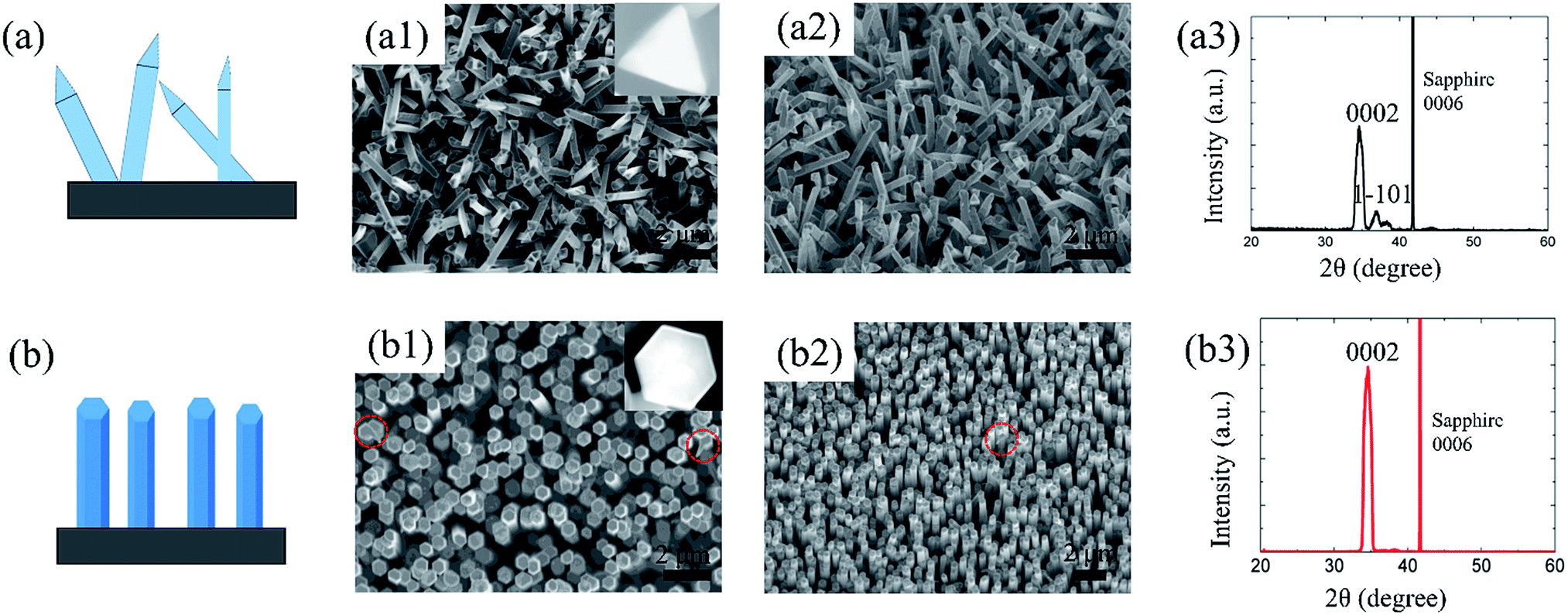 | ||
| Fig. 1 The schematic crystal models (a and b). Top (a1 and b1) and tilted view (a2 and b2) SEM images, and XRD patterns (a3 and b3) of the GaN NWs grown on c-plane sapphire with GaCl precursor flow rate to be: (a) 9 sccm (b) 16 sccm. The insets a1 and b1 present the cross-section of the NWs. Red circles in b1 and b2 show kinked structures. | ||
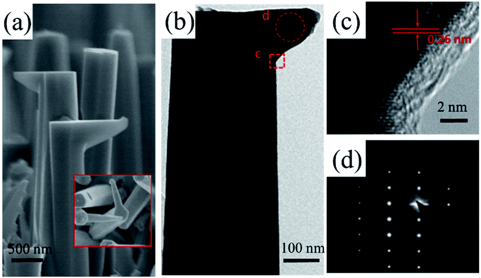
The detailed morphology and crystal structure of the GaN NWs were further analysed using the HRTEM. The GaN NWs were separated from the as-grown substrate by sonication and casted on the micro-grid. Fig. 2 shows the low-, high-resolution TEM and corresponding SAED images of NWs obtained with GaCl flow of 9 sccm (a)–(c) and 16 sccm (d)–(f), respectively. More than 10 triangular NWs were surveyed and showed that all of the NWs are grown along m-axis. Generally, low-magnification TEM images in Fig. 2(a) and (d) demonstrate that all of the NWs are little tapered with a relative smooth sidewall surface. The clear lattice fringe characteristics from the high-magnification TEM in Fig. 2(b) and (e) suggest that the NWs are single crystals with almost no dislocation. The corresponding SAED images taken along c-axis and m-axis in Fig. 2(c) and (f) confirm that these NWs are grown along m-axis and c-axis, respectively. Thus, the HRTEM results clearly confirm that the growth orientation of GaN NWs is varied when the GaCl flow rate is increased. The SEM and TEM images in Fig. 1 and 2 show that these NWs have diameter of large than 300 nm. This is due to the lateral growth on NW sidewalls (the details see follow parts).
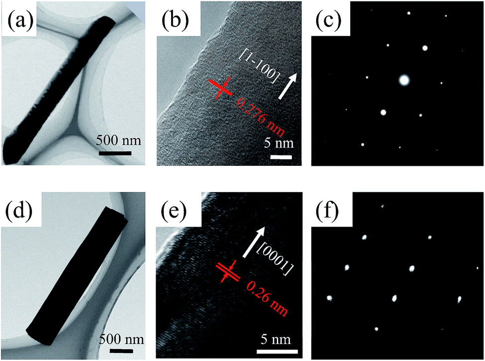 | ||
| Fig. 2 TEM images of m- and c-axis GaN NWs, which is obtained with GaCl flow of (a)–(c) 9 sccm, (d)–(f) 16 sccm respectively. Low- and high-magnification TEM is shown in a, d and b, e. The corresponding SAED is shown in c and f. | ||
The effect of substrate and metal catalyst thickness
Considering the crucial importance of substrate in NW synthesis,2,8,10 the influence of substrate on the growth orientation of GaN NWs is also investigated. Here, we grow GaN NWs on various substrates, including (111) silicon, m-sapphire and (0001) GaN with GaCl flow of 9 sccm and 16 sccm (see S1, ESI†). It is found that the triangular cross section NWs are obtained under a relatively lower GaCl flow rate whereas a higher GaCl flow is favourable for hexagonal cross section c-axis NWs, regardless of the substrate used. Consider the epitaxial orientation relationship between NWs and the substrate, the c-axis NWs result from a preferential growth normal to the GaN wafer (0001). They are inclined with an angle of 58.41° to the surface of m-plane sapphire.24 However, the c-axis NWs are tilt grown on the silicon substrate with a random growth direction due to the large lattice mismatch between the silicon substrate and GaN. These results indicate that the substrates don't have an effect to determine the NWs crystallographic orientation.To obtain NWs with high aspect ratio and also gain deep insight into the GaN NWs growth, the thickness of Ni/Au catalyst metal was increased to 2/2 nm and 4/4 nm. As shown in Fig. 3, compared to the NWs catalysed by 1/1 nm-thick Ni/Au (shown in Fig. 1), the aspect ratio and density of the GaN NWs becomes larger when the Ni/Au thickness is increased. For the GaN NWs grown under a lower GaCl flow rate (9 sccm) with the Ni/Au thickness of 2/2 nm [Fig. 4(a)], the NWs also exhibits a triangular cross-section and inclined to the substrate, which is the same with the NWs catalysed by 1/1 nm Ni/Au. In contrast, the diameter of the NWs is decreased to nearly 100 nm with the longest NW length increased to nearly 10 μm. Similarly, most of the GaN NWs grown under a higher GaCl flow rate (16 sccm) are vertical to the substrate, exhibiting a hexagonal cross-section with the diameter of NW tips is decreased from 600 nm to less than 200 nm when the thickness of Ni/Au increased to 2/2 nm and 4/4 nm [Fig. 3(b) and (c)]. Consistent to others report,25 we suggest that the increasing of Ni/Au thickness will increase the density of catalyst metal dots and thus inhibit the lateral growth. Moreover, we also suggest that the increasing of the catalyst size will increase the time for catalyst consumption, which also promotes the NW axial growth and inhibits the lateral growth.
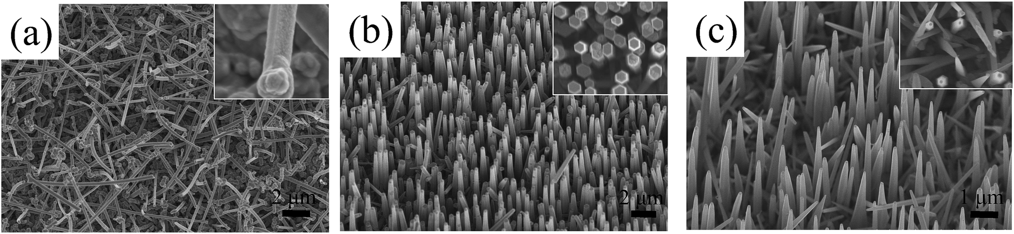 | ||
| Fig. 3 The effect of metal catalyst thickness on GaN NWs growth on c-plane sapphire: (a) and (b) SEM images of GaN NWs grown on: 4 nm Ni/Au with GaCl flow 9 sccm and 16 sccm, respectively. (c) and (d) SEM images and TEM images of GaN NWs grown on 8 nm Ni/Au with GaCl flow 16 sccm. Inset of the pictures show the cross section of GaN NWs. | ||
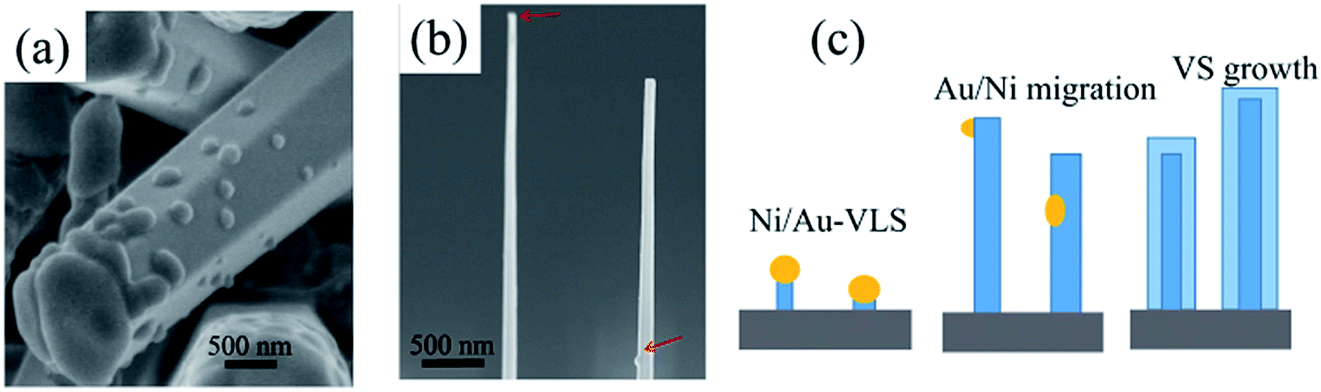 | ||
| Fig. 4 (a) Ga-droplet on NWs tip by not introducing NH3 gas during the cooling down process. (b) Au/Ni seed migration on the NW sidewall. (c) The growth process of thick GaN NWs including Ni/Au-catalyzed growth, Au/Ni migration and consumption, Ga-catalyzed growth. | ||
Except for the vertical c-axis NWs, the top view SEM image [inset Fig. 3(c)] demonstrates that some triangular cross sectioned GaN NWs are observed when the thickness of Ni/Au film is 4/4 nm even though the NWs were grown with a high GaCl flow rate. The HRTEM observations (S2, ESI†) show that all the NWs crystal quality are excellent with a tapered morphology along the growth axis with the growth orientations are c-axis (hexagonal) and m-axis (triangular). It has been reported that the NW growth orientation is catalyst size-dependent.26,27 However, although the m-axis NWs were grown when the catalyst size is very large (nearly 200 nm, by evaluating the particle size by annealing Ni/Au film under the HVPE system), we cannot speculate the GaN NWs have a size effect. We have shown that the m-axis NWs are grown under a relatively low GaCl flow rate. Popular views have suggested the low Ga flux indicates a small droplet size.28 That is to say, the increasing of droplet size by increasing of the GaCl flow rate and Ni/Au size has an opposite effect on the growth orientation of GaN NWs. In the next part, a reasonable explanation will be proposed and suggested that the NW growth orientation is catalyst composition determined.
The mechanism and kinked structures
We have demonstrated that the NWs crystallographic orientation can be manipulated by modulating the flow rate and excluded the effects from substrate and droplet size. It should be pointed out that even though we can't find any metal droplets for the thick hexagonal c-axis NWs (Fig. 1), we still conclude that all of the NWs are governed by a VLS mechanism. Firstly, we can't obtain any NWs without metal catalyst and it also has shown the thick of Au/Ni film also has a large effect for NWs morphology, especially for the diameter of the NWs. Secondly, if we don't introduce NH3 into the reactor during the cooling down process, a droplet can be observed on NWs tip [Fig. 4(a)]. The EDX was used to analysis the droplet which shown, as the self-catalyzed, Ga-induced NW growth, the droplet was composed of gallium elements whereas the nickel and gold elements were not observed. However, it can't be concluded that the thick NWs were grown by a single self-catalyzed growth mechanism. The reasonable explanation is that all of the NWs were catalyzed growth by the Au/Ni particles in the nucleation stage [Fig. 4(c)]. Then, the metal seeds on NWs' tip will be etched by the HCl gas or migrates to NW sidewall and substrate during NWs growth [Fig. 4(b)].32 At the same time, the NW tips will spontaneously form gallium droplets that will further promote the growth of NWs. However, this self-catalyzed growth process will have a large lateral growth on NW sidewall which leads to a large NW diameter.Recently, catalyst engineering on the composition, geometry, size, and position of the catalyst has been used to achieving a controllable NWs growth and realizing novel structures.6,28–32 Wang et al.29 suggested that the III-element composition affects the liquid–vapor interface energy and determines the growth orientation of NWs. They demonstrated that the InP NWs growth direction can be manipulated using MOCVD by in situ varying the supply of III precursors. Kuykendall et al.6 have obtained single-crystalline NWs along m-axis via MOCVD by using a gold-rich catalyst whereas NWs along the a-axis were obtained by adopting a nickel-rich catalyst instead. They suggested that the catalyst composition alters the liquid–solid interfacial energy and determines the NWs growth direction. In our case, compared between the surface energy of Ga-element and catalytic metals Au and Ni, we found that the liquid–vapor surface energy of Ga is much smaller (0.72 J m−2)33 than that of Au or Ni (1.16 J m−2, 1.77 J m−2).29,33 This indicates that altering the Ga-elements composition in the droplets, instead of proportion of Ni and Au, should affect more significantly on the surface energy (liquid–vapor energy or liquid–solid energy). As the Ga-element composition in the catalyst is mainly determined by the Ga precursor flow, we suggest that the GaCl flow rate determined NWs growth orientation is the result of changing of catalyst composition, which affects the nucleated surface energy. However, for accurate understanding the nucleation process, further experiments and calculations should be conducted. Some NWs with m-axis appeared in the above mentioned experiments when the Ni/Au particles were very large even though under a high Ga precursor flow. Here, we suggest the large particles may be more difficult to form high concentration Ga because these particles need more time or more Ga to develop Au–Ni–Ga droplets.34,35 Thus, at the initial nucleation stage, the composition of Ga-element in the droplet is low, which leads to the non-polar maxis GaN NW growth.
Furthermore, a new-type kinked structure occurs occasionally on some c-axis NWs which have been marked by red circles in Fig. 1. We also further purposely changed the GaCl flow rate from 16 sccm to 9 sccm during the NWs growth and observed the proportion of these kinks could be increased to 20%. This kinked NW is composed of a stand c-axis nanocone base and a horizontal m-axis wire with a 90° transition in the growth direction, that is, the crystallographic orientation of the NWs is varied during the growth [Fig. 5(a)]. The m-axis NWs are homogeneous epitaxial grown on one of the m-facets of the stand rods with the bottom diameter is the same or less than the side facets [inset Fig. 5(a)]. As show from the TEM images in Fig. 5(b)–(d), the clear GaN (0002) lattice fringes show that the kink is vertical to c-axis with a perfect epitaxy relationship to side facets of the c-axis trunk. This indicates that the kinked region of the GaN nanostructure is free of defects, which is different from the kinked nanostructures previously reported.36–38 It has been reported that defects including twin planes and stacking faults play an important role in promoting the formation of kinked structures.36–38 In our case, we suggest that some of the droplets are spread at the sidewall facets which continue to catalyst the NWs growth and form this kinked structures.
 | ||
| Fig. 5 GaN NW crystallographic orientation transition during growth: (a) side-view SEM image of kinked NW structures grown on c-plane sapphire. (b)–(d) Low and high magnification TEM images and SAED pattern illustrating growth direction switching. The inset (a) presents the tilted view of a kinked NW. The SAED pattern confirms the branch NWs are homoepitaxial grown on the stand rod. | ||
Optical properties of GaN nanowires along different crystallographic orientations
The optical properties of the NWs with different crystallographic orientations were examined using μ-PL measurements at room temperature. The PL curve of four samples grown under different conditions were shown in Fig. 6(a): 9 sccm GaCl flow rate using 1/1 nm and 2/2 nm Ni/Au (blue and red line), 16 sccm GaCl flow rate with 1/1 nm and 4/4 nm Ni/Au (gray and black line). The corresponding NW morphology are shown in Fig. 1 and 3 where all of the NWs were grown on c-plane sapphire. The results show that the NWs lateral growth is closely correlated with the optical properties of the GaN NWs. The NWs grown with a substantial lateral growth (with a thin catalyst Ni/Au film) exhibits a low crystal quality with a weak NBE emission band near 385 nm and an observable red emission centred at around 660 nm [blue and gray line, Fig. 6(a)]. On the other hand, by inhibiting the lateral growth upon increasing the metal thickness to 2/2 nm and 4/4 nm, the as grown NWs exhibit a strong NBE (near-band-edge) band centred near 370 nm, a weak defect peak centred at 560–630 nm and a faint second NBE band near 735 nm [red and black line, Fig. 6(a)]. In fact, we have conducted a series of PL measurements on different substrates. And, the results are similar—that is, the NWs lateral growth is closely correlated with the optical properties of the GaN NWs regardless of the substrate used. Although the TEM observations have shown that all of the GaN NWs are with high quality without observable dislocations (Fig. 2 and S2, ESI†), we suggest the VS lateral growth may introduce the point defects and impurities that forms the deep acceptors level, contributing to the red luminescence.39,40 A detailed study of this relationship has been published in our recently paper.41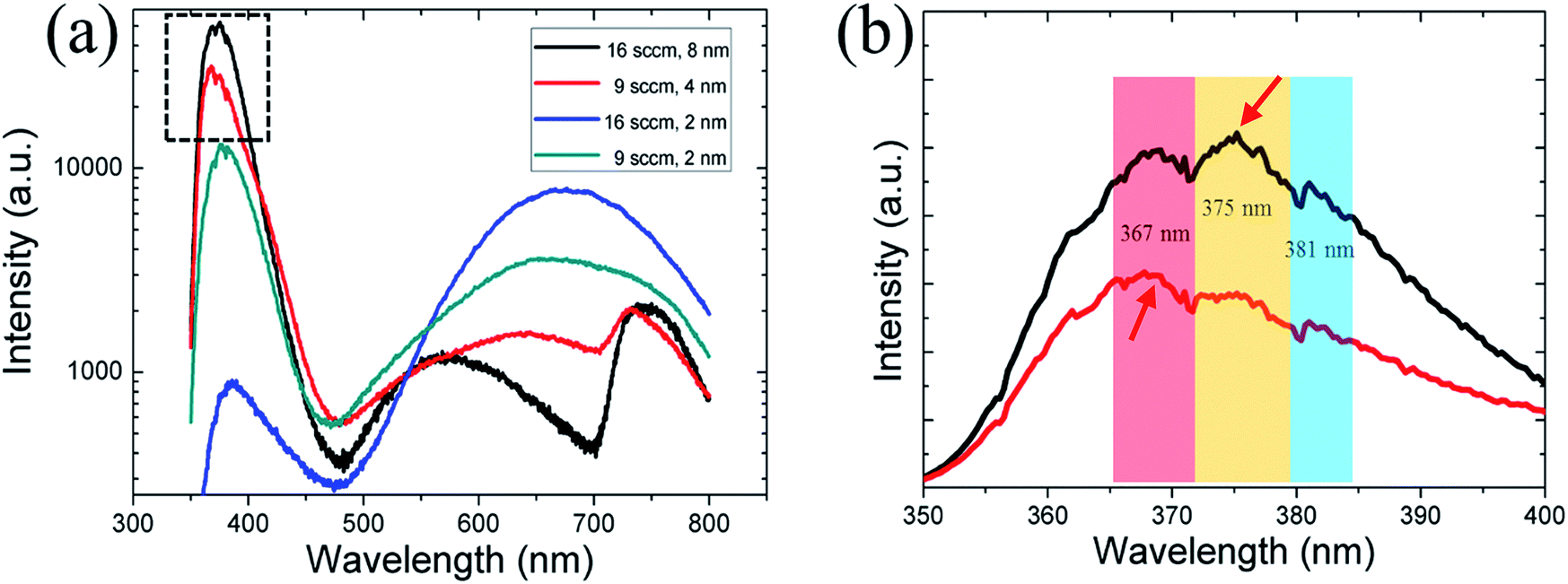 | ||
| Fig. 6 Photoluminescence (PL) measurements of different crystallographic orientation GaN NWs grown on c-plane sapphire: (a) under GaCl flow of 9 sccm (blue, Au/Ni: 1/1 nm), 9 sccm (red, Au/Ni: 2/2 nm), 16 sccm (gray, Au/Ni: 1/1 nm), 16 sccm (black, Au/Ni: 4/4 nm); (b) a high-resolution PL spectrum of the dotted box area in (a) in a linear scale. | ||
Furthermore, the growth orientation was observed to affect the optical properties of the GaN NWs. For GaN NWs grown under a thin Ni/Au film of 1/1 nm, even though the c-axis NWs were grown with a substantial lateral growth (with diameter over 500 nm) than the m-axis NWs (with diameter of nearly 300 nm), the material quality is demonstrated to be better, as revealed by PL results. The intensity ratios between the red luminescence and NBE for the thick c-axis NWs is 4, which is larger than the value of 0.3 for the thick non-polar NWs. On the other hand, for the NWs with limited lateral growth (grown under a thick Ni/Au film), the NBE peak of the thin non-polar NWs exhibit an 8 nm (∼72 meV) blue shift compared with that of the c-axis NWs [Fig. 6(a)]. The previous study have shown that the PL peak of the non-polar NWs blue shifts compared with the NWs with polar c-axis, which is due to spontaneous polarization in GaN.10,42 However, a careful observation [Fig. 6(b)] show that the shift is not due to the band gap variations, but related to competition of two peaks located at 367 nm and 375 nm. As shown in the UV band, three peaks at 367 nm, 375 nm and 380 nm are observed. Here, the peaks at 367 nm is a common band-edge emission for n-typed GaN whereas the latter two peaks (375 nm and 381 nm) are attributed to the surface or impurity-related emission.43,44 Yi et al.44 have reported a similar PL spectrum where three peaks (366 nm, 372 nm and 380 nm) were observed in the UV band for the HVPE-grown GaN film. They suggested that the 372 nm and 380 nm peak represent an impurity-related with oxygen, and a donor–acceptor pair recombination, respectively. In our experiment, we suggest the oxygen which remains in the HVPE chamber will affect the NW quality and correlate with the peak at 375 nm. The different relative intensity of band-edge emission/oxygen-related emission between the polar and non-polar GaN NWs might be due to the difference of exposed facets which affect the doping of oxygen. It should be pointed out that the PL curves are not smooth and with many weak lines which are related to the noise or/and other radiative recombination.39 Finally, the strong UV emissions PL spectra of the NWs with a limited lateral growth confirm that the grown NWs have good optical properties and may be advantageous for using as build blocks for nano-optoelectronic devices in the near future.
Conclusions
To conclude, we have demonstrated the manipulation of crystallographic orientation of GaN NWs using VLS-HVPE. By turning the metal III-precursor flow rate, the growth orientation of GaN NWs can be varied from polar c-axis to non-polar m-axis. This approach can be applied on various substrates, including c-, r-plane, m-plane sapphire, (111) silicon and (0001) GaN, which validates the versatility of the proposed approach and also confirms that the crystallographic orientation of the grown GaN NW is not epitaxial determined. Moreover, the optical properties of GaN NWs were characterized using PL, revealing that the observed red luminescence (located near 660 nm) arises from the highly lateral-grown layer of the GaN NWs. Our reports provide a meaningful approach to manipulate the GaN NWs growth orientation and would significantly advance the development of GaN NWs based optoelectronics and photonics devices.Conflicts of interest
There are no conflicts to declare.Acknowledgements
This work was supported by National Key R&D Program of China (Grant No. 2017YFB0403100, 2017YFB0403101), National Natural Science Foundation of China (U1505253, 61306051 and 61306050).Notes and references
- R. S. Wagner and W. C. Ellis, Appl. Phys. Lett., 1964, 4, 89 CrossRef CAS.
- S. A. Fortuna and X. Li, Semicond. Sci. Technol., 2010, 25, 24005 CrossRef.
- Y. Wang, V. Schmidt, S. Senz and U. Gosele, Nat. Nanotechnol., 2006, 1, 186–189 CrossRef CAS PubMed.
- E. P. Bakkers, J. A. Dam, F. S. De, L. P. Kouwenhoven, M. Kaiser, M. Verheijen, H. Wondergem and P. V. D. Sluis, Nat. Mater., 2004, 3, 769–773 CrossRef CAS PubMed.
- T. Kuykendall, P. Auzauskie, S. K. Lee, Y. F. Zhang, J. Goldberger and P. D. Yang, Nano Lett., 2003, 3, 1063–1066 CrossRef CAS.
- T. R. Kuykendall, M. V. Altoe, D. F. Ogletree and S. Aloni, Nano Lett., 2014, 14, 6767–6773 CrossRef CAS PubMed.
- K. Lekhal, G. Avit, Y. Andre, A. Trassoudaine, E. Gil, C. Varenne, C. Bougerol, G. Monier and D. Castelluci, Nanotechnology, 2012, 23, 40560 CrossRef PubMed.
- G. T. Wang, A. A. Talin, D. J. Werder, J. R. Creighton, E. Lai, R. J. Anderson and I. Arslan, Nanotechnology, 2006, 17, 5773 CrossRef CAS.
- J.-H. Park, A. Mandal, D.-Y. Um, S. Kang, D.-s. Lee and C.-R. Lee, RSC Adv., 2015, 5, 47090–47097 RSC.
- T. Kuykendall, P. J. Pauzauskie, Y. Zhang, J. Goldberger, D. Sirbuly, J. Denlinger and P. Yang, Nat. Mater., 2004, 3, 524–528 CrossRef CAS PubMed.
- Y. Huang, X. Duan, Y. Cu and M. C. Lieber, Nano Lett., 2002, 2, 101–104 CrossRef CAS.
- R. Yan, D. Gargas and P. Yang, Nat. Photonics, 2009, 3, 569–576 CrossRef CAS.
- S. Li and A. Waag, J. Appl. Phys., 2012, 111, 071101 CrossRef.
- C. Li, J. B. Wright, S. Liu, P. Lu, J. J. Figiel, B. Leung, W. W. Chow, I. Brener, D. D. Koleske, T. S. Luk, D. F. Feezell, S. R. Brueck and G. T. Wang, Nano Lett., 2017, 17, 1049–1055 CrossRef CAS PubMed.
- C. Chèze, L. Geelhaar, B. Jenichen and H. Riechert, Appl. Phys. Lett., 2010, 97, 153105 CrossRef.
- J. B. Schlager, K. A. Bertness, P. T. Blanchard, L. H. Robins, A. Roshko and N. A. Sanford, J. Appl. Phys., 2008, 103, 124309 CrossRef.
- S. D. Hersee, X. Y. Sun and X. Wang, Nano Lett., 2006, 6, 1808 CrossRef CAS PubMed.
- B. O. Jung, S. Y. Bae, Y. Kato, M. Imura, D. S. Lee, Y. Honda and H. Amano, CrystEngComm, 2014, 16, 2273–2282 RSC.
- D. Tsivion, M. Schvartzman, R. Popovitz-Biro, H. P. Von and E. Joselevich, Science, 2011, 333, 1003–1007 CrossRef CAS PubMed.
- G. Avit, K. Lekhal, Y. Andre, C. Bougerol, F. Reveret, J. Leymarie, E. Gil, G. Monier, D. Castelluci and A. Trassoudaine, Nano Lett., 2014, 14, 559–562 CrossRef CAS PubMed.
- E. Gil, V. G. Dubrovskii, G. Avit, Y. Andre, C. Leroux, K. Lekhal, J. Grecenkov, A. Trassoudaine, D. Castelluci, G. Monier, R. M. Ramdani, C. Robert-Goumet, L. Bideux, J. C. Harmand and F. Glas, Nano Lett., 2014, 14, 3938–3944 CrossRef CAS PubMed.
- Q. Li, Y. Lin, J. R. Creighton, J. J. Figiel and G. T. Wang, Adv. Mater., 2009, 21, 2416–2420 CrossRef CAS.
- R. A. Burke, D. R. Lamborn, X. Weng and J. M. Redwing, J. Cryst. Growth, 2009, 311, 3409 CrossRef CAS.
- K. Lee, S. Chae, J. Jang, D. Min, J. Kim, D. Eom, Y. S. Yoo, Y. H. Cho and O. Nam, Nanotechnology, 2015, 26, 335601 CrossRef PubMed.
- H. Xu, Y. Wang, Y. Guo, Z. Liao, Q. Gao, N. Jiang, H. H. Tan, C. Jagadish and J. Zou, Cryst. Growth Des., 2012, 12, 2018–2022 CAS.
- V. Schmidt, S. Senz and U. Gosele, Nano Lett., 2005, 5, 931–935 CrossRef CAS PubMed.
- Y. Cai, S. K. Chan, I. K. Sou, Y. F. Chan, D. S. Su and N. Wang, Adv. Mater., 2006, 18, 109–114 CrossRef CAS.
- S. Crawford, S. K. Lim and S. Gradecak, Nano Lett., 2013, 13, 226–232 CrossRef CAS PubMed.
- J. Wang, S. R. Plissard, M. A. Verheijen, L. F. Feiner, A. Cavalli and E. P. Bakkers, Nano Lett., 2013, 13, 3802–3806 CrossRef CAS PubMed.
- S. R. Plissard, I. V. Weperen, D. Car, M. A. Verheijen, G. W. G. Immink, J. Kammhuber, L. J. Cornelissen, D. B. Szombati, A. Geresdi, S. M. Frolov, L. P. Kouwenhoven and E. Bakkers, Nat. Nanotechnol., 2013, 8, 859–864 CrossRef CAS PubMed.
- D. Jacobsson, F. Panciera, J. Tersoff, M. C. Reuter, S. Lehmann, S. Hofmann, K. A. Dick and F. M. Ross, Nature, 2016, 531, 317–322 CrossRef CAS PubMed.
- F. Panciera, M. M. Norton, S. B. Alam, S. Hofmann, K. Molhave and F. M. Ross, Nat. Commun., 2016, 7, 12271–12276 CrossRef CAS PubMed.
- I. Egry, E. Ricci, R. Novakovic and S. Ozawa, Adv. Colloid Interface Sci., 2010, 159, 198–212 CrossRef CAS PubMed.
- B. J. Kim, J. Tersoff, S. Kodambaka, M. C. Reuter, E. A. Stach and F. M. Ross, Science, 2008, 322, 1070–1073 CrossRef CAS PubMed.
- S. A. Dayeh and S. T. Picraux, Nano Lett., 2010, 10, 4032–4039 CrossRef CAS PubMed.
- S. A. Dayeh, J. Wang, N. Li, J. Y. Huang, A. V. Gin and S. T. Picraux, Nano Lett., 2011, 1, 4200–4206 CrossRef PubMed.
- K. Hillerich, K. A. Dick, C. Y. Wen, M. C. Reuter, S. Kodambaka and F. M. Ross, Nano Lett., 2013, 13, 903–908 CrossRef CAS PubMed.
- E. Uccelli, J. Arbiol, C. Magen, P. Krogstrup, E. Russo-Averchi, M. Heiss, G. Mugny, F. Morier-Genoud, J. Nygard, J. R. Morante and I. M. A. Fontcuberta, Nano Lett., 2011, 11, 3827–3832 CrossRef CAS PubMed.
- M. A. Reshchikov and H. Morkoc, J. Appl. Phys., 2005, 97, 061301 CrossRef.
- L. Wang, E. Richter and M. Weyers, Phys. Status Solidi C, 2010, 204, 846–853 CrossRef.
- S. T. Wu, L. C. Wang, X. Y. Yi, Z. Q. Liu, T. B. Wei, G. D. Yuan, J. X. Wang and J. M. Li, J. Appl. Phys., 2017, 122, 205302 CrossRef.
- H. Li, A. Chin and M. Sunkara, Adv. Mater., 2006, 18, 216–220 CrossRef CAS.
- K. Choi, M. Arita and Y. Arakawa, J. Cryst. Growth, 2012, 357, 58–61 CrossRef CAS.
- S. N. Yi, H. S. Ahn, M. Yang, K. H. Kim, H. Kim, J. Y. Yi, J. H. Chang and H. S. Kim, J. Korean Phys. Soc., 2004, 45, S598–S600 CAS.
Footnote |
| † Electronic supplementary information (ESI) available: More SEM and TEM images of the GaN NWs (S1 and S2). See DOI: 10.1039/c7ra11408g |
| This journal is © The Royal Society of Chemistry 2018 |