
 Open Access Article
 This Open Access Article is licensed under a
 Creative Commons Attribution 3.0 Unported Licence
Investigation on cation distribution and luminescence in spinel phase γ-Ga3−δO4![[thin space (1/6-em)]](https://www.rsc.org/images/entities/h2_char_2009.gif) :Sm nanostructures using X-ray absorption spectroscopy†
:Sm nanostructures using X-ray absorption spectroscopy†
Aditya Sharma *a,
Mayora Varshneya,
Hyun-Joon Shinb,
Keun Hwa Chaea and
Sung Ok Won*a
*a,
Mayora Varshneya,
Hyun-Joon Shinb,
Keun Hwa Chaea and
Sung Ok Won*a
aAdvanced Analysis Centre, Korea Institute of Science and Technology, Seoul-02792, South Korea. E-mail: adityaiuac@gmail.com; sowon@kist.re.kr
bPohang Accelerator Laboratory (POSTECH), Pohang-37673, South Korea
First published on 14th November 2017
Abstract
In this study, spectroscopic investigations are employed to quantify the Ga distribution over the tetrahedral/octahedral sites and to assimilate the luminescence properties in the barely reported γ-Ga2.67O4![[thin space (1/6-em)]](https://www.rsc.org/images/entities/char_2009.gif) :Sm nanoparticles. O K-edge XANES are convincing the decreased electron density in the outermost hybrid orbits of O 2p and Ga 4p, and the movement of p electrons to the inner hybrid orbits with s character under the distorted oxygen environment of γ-Ga2.67O4:Sm nanoparticles. The Ga K/L-edge XANES and Sm L3/M5,4-edge XANES results have confirmed Ga3+ and Sm3+ ions, respectively, in the γ-Ga2.67O4:Sm nanoparticles. Quantitative determination of the cation distribution is performed by applying Ga K-edge XANES data analysis, which is further substantiated by an EXAFS data simulation, and conveys a Ga-O4 tetrahedra/Ga-O6 octahedra ratio (Ga(t)/Ga(o)) of ∼0.9, ∼1.4, ∼1.5 and ∼1.6 for the β-Ga2O3, γ-Ga2.67O4, γ-Ga2.67O4:5Sm and γ-Ga2.67O4:10Sm samples, respectively, which signify the Sm doping induced deformation of Ga-O6 octahedra via the formation of oxygen defects. Multiple luminescence centres, facilitated by the Ga-O6 octahedra distortion, O vacancies and Sm3+ ions, have helped in a significant enhancement of the emission characteristics. Our spectroscopy investigations, with the help of XANES and EXAFS, may open new opportunities to the mechanistic understanding of metal-O polyhedra alteration induced fruition of physical/chemical properties in the less explored meta stable phases of other complex oxides.
:Sm nanoparticles. O K-edge XANES are convincing the decreased electron density in the outermost hybrid orbits of O 2p and Ga 4p, and the movement of p electrons to the inner hybrid orbits with s character under the distorted oxygen environment of γ-Ga2.67O4:Sm nanoparticles. The Ga K/L-edge XANES and Sm L3/M5,4-edge XANES results have confirmed Ga3+ and Sm3+ ions, respectively, in the γ-Ga2.67O4:Sm nanoparticles. Quantitative determination of the cation distribution is performed by applying Ga K-edge XANES data analysis, which is further substantiated by an EXAFS data simulation, and conveys a Ga-O4 tetrahedra/Ga-O6 octahedra ratio (Ga(t)/Ga(o)) of ∼0.9, ∼1.4, ∼1.5 and ∼1.6 for the β-Ga2O3, γ-Ga2.67O4, γ-Ga2.67O4:5Sm and γ-Ga2.67O4:10Sm samples, respectively, which signify the Sm doping induced deformation of Ga-O6 octahedra via the formation of oxygen defects. Multiple luminescence centres, facilitated by the Ga-O6 octahedra distortion, O vacancies and Sm3+ ions, have helped in a significant enhancement of the emission characteristics. Our spectroscopy investigations, with the help of XANES and EXAFS, may open new opportunities to the mechanistic understanding of metal-O polyhedra alteration induced fruition of physical/chemical properties in the less explored meta stable phases of other complex oxides.
Introduction
Gallium-oxide (Ga2O3) polymorphs i.e.; α-Ga2O3, β-Ga2O3, γ-Ga2O3, δ-Ga2O3 and ε-Ga2O3,1–4 have evoked much attention because of their wide range of applications in optoelectronics, gas sensing, magnetic tunnel junctions, photo-catalysis, biomedical fields, etc.5–9 Among all the known phases of Ga2O3, γ-Ga2O3 is the class of material which possesses a cubic or defective-spinel crystal structure with uneven occupancy of Ga at the tetrahedral and octahedral sites.2–4 The strong correlation between the metal atom site occupancy and its structural/optical/electronic properties make γ-Ga2O3 an attractive material for investigating the fundamental connections between the crystal/electronic structure and unexplored applications.Most of the reports on γ-Ga2O3 have considered the cubic unit cell of this compound;8,10–12 however, a defective spinel structure of γ-Ga2O3 (space group; Fd![[3 with combining macron]](https://www.rsc.org/images/entities/char_0033_0304.gif) m) was recently identified by a neutron diffraction technique with four different site occupancies of Ga: tetrahedral (8a), octahedral (16d), tetrahedral (48f) and octahedral (16c).3,4 Unlike the normal spinel-structure stoichiometry in γ-Ga2O3 (ideally, it should be Ga3O4), among every 18 cationic sites, two sites are vacant in order to retain charge neutrality.3,4 Pair distribution function analysis was also employed to refine the γ-Ga2O3; however, the discrepancy between the average and local structure could not be resolved.4 If such complications were not enough during the simulation of the γ-Ga2O3 structural details, investigations on the local structure determination would further be complicated in the cation deficient spinel phases of gallium oxides, such as γ-Ga3−δO4. The cation deficient γ-Ga3−δO4 phase is very similar to that of a hypothetical spinel Ga3O4 compound; however, less investigation has been made because of its poor thermal stability during its synthesis.
m) was recently identified by a neutron diffraction technique with four different site occupancies of Ga: tetrahedral (8a), octahedral (16d), tetrahedral (48f) and octahedral (16c).3,4 Unlike the normal spinel-structure stoichiometry in γ-Ga2O3 (ideally, it should be Ga3O4), among every 18 cationic sites, two sites are vacant in order to retain charge neutrality.3,4 Pair distribution function analysis was also employed to refine the γ-Ga2O3; however, the discrepancy between the average and local structure could not be resolved.4 If such complications were not enough during the simulation of the γ-Ga2O3 structural details, investigations on the local structure determination would further be complicated in the cation deficient spinel phases of gallium oxides, such as γ-Ga3−δO4. The cation deficient γ-Ga3−δO4 phase is very similar to that of a hypothetical spinel Ga3O4 compound; however, less investigation has been made because of its poor thermal stability during its synthesis.
Theoretical studies have shown that the band structure of Ga2O3, near the Fermi level, is formed by the O 2p and Ga 4s states. The top of the valence band consists mainly of the O 2p states, with a width of 7 eV, and the bottom of the conduction band is formed by Ga 4s states.13–15 Ga d orbitals do not contribute to the band structure near the Fermi level, because of the 3d10 electronic configuration of Ga d orbitals in Ga2O3, but facilitate a deep valence band along with the O 2s orbitals.13,14 The octahedrally coordinated Ga atoms possess higher coordination with the surrounding O atoms, compared with the tetrahedrally coordinated Ga atoms, and, thus, the degree of covalency is higher for the tetrahedrally coordinated Ga atoms in the Ga2O3 lattice.13–15 The band structure and, hence, the electronic/optical properties of Ga2O3 are not only sensitive to the doping of foreign element at Ga lattice sites16,17 but may also be detonated by the distortion of the Ga–O environment or alteration in the Ga site occupancy. A small change in the Ga tetrahedral/octahedral site occupancy is expected to affect the orbital hybridization of frontier Ga 4s/4p and O 2p orbitals which, obviously, can regulate the band structure of the compound and consequently electronic/optical properties.
In the previous reports, nano/micro sized β-Ga2O3 particles have been extensively studied for their synthesis,9,18–23 band structure,15 optical18,19 and catalyst properties.21–23 The other polymorphous phases of gallium oxide can demonstrate exceptional metal–oxygen orbital hybridization and a perceptibly diverse band structure near the Fermi level because of the miscellaneous Ga site occupancy in the Ga2O3 lattice; however, their synthesis, crystal structure analysis, optical properties and local atomic/electronic structure investigations are ineffectually reported. Thus, an atomistic level investigation on the unidentified or less studied polymorphous phases, such as the cation deficient γ-Ga3−δO4, is desirable to gain control over and fabricate their nanostructures for light-emitting applications. Though the synthesis of small sized nanostructures is important for catalytic21–23 and optical properties,10–12,18–20 the tiny nanostructures introduce complications in the structural and electronic structure investigations because of the significant surface artefacts.10–12,18–20 The sensitivity of the powder XRD techniques becomes poor to the structural details when the particle size reaches up to a few nanometres.24,25 Moreover, for the case of nanocrystalline Ga2O3 polymorphs, the diverse occupancies of Ga atoms and cation/anion deficiencies facilitate a complex local atomic structure to the compound which may not be completely elucidated by the conventional XRD technique.2,3 Therefore, it is necessary to apply modern techniques which not only probe the crystal structure ‘locally’ but also provide valuable information on the lattice disorders upon defect formation, foreign element doping and alteration in the metal element occupancy. In this regard, X-ray absorption spectroscopy (XAS), with its two branches of X-ray absorption near edge structure (XANES) and extended X-ray absorption fine structure (EXAFS), becomes the important elemental characterization technique and has been known to be highly sensitive to the local electronic/atomic structure properties and effectively overcomes the issue of sensitivity to the structure and electronic structure characterization of small sized, poorly crystalline or embedded nanostructures.26–28 In the last few years, probing the local symmetry of the diluted doped elements,29,30 quantification of the valence state changes of host metal ions upon foreign element doping,31–33 changes in the orbital occupancy,34,35 and variation in the crystal field effects36,37 have been studied for various compounds using the XANES. On the other side, EXAFS, due to the sensitivity to the local atomic structure, has become a powerful probing tool for determining the variation in the coordination number and bond lengths of the constituent elements of the probed material.32–40 Besides providing detailed experimental and simulated results on the Ga2O3 polymorphous compounds, the XANES–EXAFS analysis presented in this article addresses various aspects. Firstly, O K-edge XANES spectra were examined to specifically look into the diversity in the oxygen environment of γ-Ga3−δO4 and β polymorphous phases and to assimilate the effect of Sm insertion on the metal 4s/4p and O 2p orbital hybridization. Secondly, quantitative determination of the cation distribution is performed by using Ga K-edge XANES and EXAFS to estimate the Ga-O4 tetrahedra and Ga-O6 octahedra proportions in β-Ga2O3, γ-Ga3−δO4 and Sm doped γ-Ga3−δO4. To our knowledge, the Ga-O6/Ga-O4 octahedra/tetrahedra deformation under Sm incorporation and enhancement in the emission characteristics of γ-Ga3−δO4:Sm nanoparticles are barely covered in the literature. Our spectroscopy investigations may provide mechanistic insights into the modification in the orbital hybridization of Ga 4s/4p and O 2p, Ga local site occupancy, defect formation and emission properties of the metastable γ-Ga3−δO4 phase.
Experimental
Pure and Sm-doped gallium oxide nanoparticles were synthesized using a modified non-aqueous precipitation method. All the reagents used were of analytical grade without further purification. Pure gallium oxide nanoparticles were synthesized by dissolving 2g of Ga(NO3)2·xH2O (gallium nitrate hydrate) into 100 ml of ethanol under vigorous magnetic stirring. However, to synthesize the Sm doped gallium oxide nanoparticles, SmCl3·6H2O (samarium chloride hexahydrate) was mixed with the Ga(NO3)2·H2O, in the desired molar proportion, and then dissolved in 100 ml of ethanol with magnetic stirring for an hour. Two different molar concentrations (i.e., 5 and 10 molar percentages) of Sm3+ ions were applied in the present experiments. After achieving clear solutions of the precursors, the pH of the solution was raised up to 11 ± 0.2 by adding hydrazine monohydrate. As soon as the hydrazine monohydrate was added to the solution, an abrupt precipitation was achieved. The precipitates were washed several times with ethanol and then dried at 80 °C in air overnight. A fraction of a pure gallium oxide sample was also annealed at 600 °C and 900 °C in air for two hours. XRD measurements were performed by using the Bruker D8 advanced diffractometer, operated at a 40 kV accelerating voltage and 40 mA tube current. The radiation produced from the Cu target was Cu Kα of wavelength 1.5418 Å. Transmission electron microscopy (TEM) measurements were performed using the FEI (Tecnai-F20G2) transmission electron microscope operated at 200 kV. The Raman spectra were collected by using the Renishaw InVia Raman Microscope with a Nd:YAG (neodymium-doped yttrium aluminium garnet) laser, which produces 532 nm wavelength photon beam. XANES spectra at the O K-edge, Sm M5,4-edge and Ga L-edge were collected in the total electron yield (TEY) mode at the 10D (XAS-KIST) soft X-ray beamline at the Pohang Accelerator Laboratory (PAL), South Korea. The photon energy resolution of this beamline was better than 0.6 eV (at the O K edge). The EXAFS spectra at the Ga K-edge and Sm L3-edge were collected at the 1D XRS KIST-PAL beam line. This beam line utilizes a Si (111) double crystal monochromator and the higher harmonics were effectively removed by detuning the crystals to 70% of the maximum intensity. This beam line has three ionization chambers for collecting the data from samples, either in the transmission or fluorescence mode. Generally, the chamber, which is used for measuring the incident beam current, is filled with He. Chambers for measuring the transmission and reference spectra are filled with N2. For energy approaching 16 keV, an Ar gas or mixture of Ar and N2 is preferred for these chambers; however, a mixture of He and N2 is used when the beam energy is nearly 4 keV. N2 in the transmission and reference chamber is the best choice for measuring spectra in the energy range 5–15 keV. Energy calibrations were made for all the measurements using reference metal foils of the constituent elements in the sample. The sample was placed between the first and the second ionization chambers, while the reference foils were placed between the second and the third ionization chambers. Photoluminescence was measured by using a 325 nm He–Cd laser as the excitation source with a power density < 0.6 W m−2.
Results and discussion
X-ray diffraction, TEM and Raman studies
Fig. 1(a) shows the XRD patterns of pure, 5 mol% Sm doped, and 10 mol% Sm doped gallium oxides samples. Fig. 1(b) shows the XRD results of the 600 °C and 900 °C annealed samples. It is evident from Fig. 1(a) that the XRD patterns of the pure and Sm incorporated gallium oxide samples consist of several diffraction peaks. All the diffraction peaks of the pure and Sm doped samples were fairly matched with the cation-deficient spinel structure γ-Ga2.67O4 (space group Fdm; JCPDS#15-2085, a = b = c = 8.238 Å, α = β = γ = 90°). Thus, our XRD results conveying the formation of a cation deficient γ-Ga2.67O4 phase in the present study. Hereafter, pure, 5 mol% Sm doped, and 10 mol% Sm doped samples are named as γ-Ga2.67O4, γ-Ga2.67O4:5Sm and γ-Ga2.67O4:10Sm, respectively. In previous reports, the cubic unit cell has been extensively assigned to the γ phases of Ga2O3 with the expected distribution of Ga over the tetrahedral (8a) and octahedral (16c) sites.8,10–12 Contrary to this, we have achieved cation-defective spinel γ-Ga2.67O4 compounds in which Ga3+ ions can additionally distribute over the tetrahedral (48f) sites along with the tetrahedral (8a) and octahedral (16c) sites.4 Besides the expected Ga occupancy dissimilarity in the presented synthesized compounds, there is a distinct difference in the XRD patterns of the γ-Ga2.67O4 phase and the commonly reported γ-Ga2O3 phase. In the inset of Fig. 1(a), we provide the diffraction patterns of JCPDS#15-2085 (for the γ-Ga2.67O4 phase) and JCPDS#20-0426 (for the commonly reported γ-Ga2O3 phase). It is clear from the inset of Fig. 1(a) that the peak (111), appearing at ∼18.7°, is distinctly present in the XRD results of γ-Ga2.67O4 and JCPDS#15-2085, but not seen in JCPDS#20-0426 and previously reported cubic phasic γ-Ga2O3 nanoparticles. Synthesis of an obscured polymorphous phase of gallium oxide is intriguing and may be the consequences of non-aqueous synthesis and an implication of a highly reactive hydrazine monohydrate precursor in the present research. Hydrazine monohydrate can quickly and effectively reduce the starting reagent of Ga and form abrupt precipitation in which nuclei of gallium oxide can be formed. Such starting nuclei, if washed and filtered with ethanol (ethanol works as an effective dispersive media for the precipitates41), may grow into the cation deficient γ-Ga2.67O4 phase upon a low-temperature drying process (80 °C).
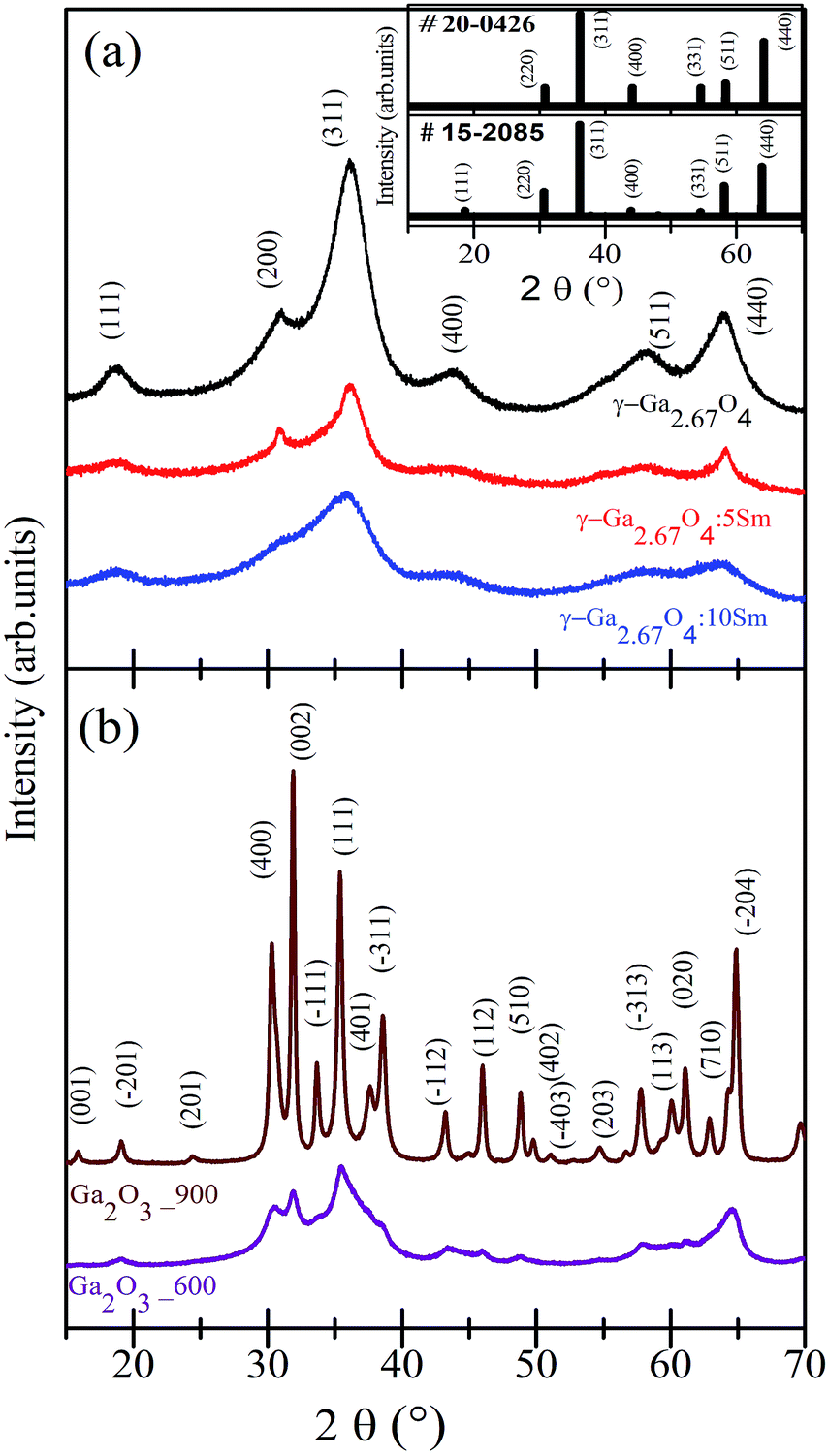 | ||
| Fig. 1 (a) XRD patterns of pure and Sm doped γ-Ga2.67O4. (b) XRD patterns of the samples annealed at 600 °C and 900 °C. Spectra are vertically shifted for clarity of the data. | ||
In previous reports, synthesis with DI water and liquid ammonia solution could only grow GaOOH kinds of phases which further transformed into α-Ga2O3, γ-Ga2O3 and β-Ga2O3 phases upon high-temperature annealing.18,19 Thus, the formation of the γ-Ga2.67O4 phase in the present study, at moderate temperate, is due to the modified non-aqueous synthesis procedure with the amendment of a reactive hydrazine monohydrate precursor. No diffraction peak matched with the other polymorphous of gallium oxide (i.e., α-Ga2O3, β-Ga2O3, δ-Ga2O3 and ε-Ga2O3) or trivial phases of metallic Sm, SmO and Sm2O3 and, thus, the XRD results strengthen the manufacturing of single phase γ-Ga2.67O4:Sm in the present study. Significant XRD peak broadening and diminishing of peak intensity is seen in the Sm doped samples and could be due to a decrease of particle size and/or lattice deformation. We have calculated the crystallite size from all of the samples using the Scherrer relation; D = 0.9λ/βCosθ (D is the particle size, λ is the wavelength of the X-rays used, β is the full width at half maximum of the diffraction peak, and the instrument broadening effect was not included in such calculations). Thus, the calculated sizes are 4.3 nm, 2.9 nm, 2.1 nm, 13.2 nm and 32.5 nm for the γ-Ga2.67O4, γ-Ga2.67O4:5Sm, γ-Ga2.67O4:10Sm, 600 °C annealed and 900 °C annealed samples, respectively. The XRD patterns also give an impression that there is a lower angle shifting in the diffraction peaks of the Sm doped samples, compared with pure γ-Ga2.67O4 (this can be easily seen in the γ-Ga2.67O4:10Sm sample). Thus, d(311) was examined and found to be 2.488(6) Å, 2.495(2) Å and 2.519(2)Å for the γ-Ga2.67O4, γ-Ga2.67O4:5Sm and γ-Ga2.67O4:10Sm samples, respectively. The marginal increase in the d(311) values for Sm doped samples may arise due to the occupancy of larger Sm3+ ions (ionic radii ∼ 109.8 pm) at the lattice position of smaller Ga3+ ions (ionic radii, ∼78.0 pm). The decrease in crystallite size and increase in the d(311) values indicate the inhibition of crystalline growth and structural perturbation in the crystalline lattice of gallium oxide upon Sm3+ ion doping. Here we expect that the insertion of Sm3+ ions in the crystalline lattice of gallium oxide produces a strain (due to the larger ionic radii of Sm3+ over Ga3+) which, conceivably, alters the metal–oxygen polyhedra and leads to a decline in the crystallinity of the material. Moreover, in previous reports, doping of a foreign element evidenced the non-stoichiometry of the metal–oxygen chains or segregation of the doped ions at surface/grain boundaries, which prevents the crystalline growth of the particle.12,42 The non-stochiometric metal–oxygen grain boundaries, which can be formed by lattice-strain induced diverse metal–oxygen stacking or segregation of dopants, may increase the amorphous content in the γ-Ga2.67O4:Sm nanoparticles, leading to broadening of the XRD peaks and a decrease in the peak intensity. In our previous reports,32,33 a similar trend in the XRD peak broadening and increase in the cell parameters/d(hkl) was observed for the Eu and Hf doped CeO2 NPs and was ascribed to the Eu/Hf induced lattice disorders in CeO2. Raman measurements are also convincing of the poor crystallinity in the Sm doped samples and have also ruled out a suspected phase formation (Fig. S1 and related discussion in the ESI†). The decrease in the particle size and the poor crystallinity are also seen in the TEM and FFT images of the γ-Ga2.67O4:5Sm and γ-Ga2.67O4:10Sm samples and tally with the findings from XRD results (Fig. S2 and related discussion in the ESI†). XRD patterns in Fig. 1(b) are certainly dissimilar with respect to the XRD patterns of γ-Ga2.67O4 and suggest a different phase formation in the 600 °C and 900 °C annealed samples. XRD patterns of the 600 °C and 900 °C annealed samples are fairly matched with the monoclinic unit cell of the β-Ga2O3 phase (space group C2/m; JCPDS#02-2603). Hereafter, the 600 °C and 900 °C annealed samples are named as Ga2O3_600 and Ga2O3_900, respectively. Raman studies have also confirmed the β-Ga2O3 phase formation in the annealed sample (see Fig. S1 and related discussion in the ESI†). In previous reports, β-Ga2O3 phase formation from the other polymorphous phases was achieved at or above 550 °C.18,19 Therefore, our findings are in accordance with the reported results and are convincing of the annealing induced β-Ga2O3 phase formation in the Ga2O3_600 and Ga2O3_900 samples. Although the β-Ga2O3 phase is present in both of the annealed samples, narrower XRD peaks with a higher intensity are seen in the Ga2O3_900 sample. XRD peak intensification in the Ga2O3_900 sample is due to the growth of larger sized particles and stabilization of the β-Ga2O3 phase under the high-temperature treatment. Larger sized particles and higher crystallinity is clearly seen in the TEM and FFT images of Ga2O3_600 and Ga2O3_900 samples (see Fig. S2 and related discussion in the ESI†).
XANES studies at the O K-edge, Ga K-edge, Sm L3-edge, Ga L-edge and Sm M5,4-edge
In the case of gallium oxide, the metal d and O 2p states are filled (3d10 electronic configuration of Ga3+ in Ga2O3) and, thus, the final state corresponds to the antibonding orbitals forming from the hybridization of the O 2p state with Ga 4s and Ga 4p.44–46 Moreover, the overall spectral features of Ga2O3 polymorphous are expected to be sensitive to the environment of O atoms with respect to the Ga atoms. Fractional amounts of tetrahedral/octahedral ligand fields of the O atoms in the different phases of Ga2O3, which also depends on the Ga site occupancy, may lead to diverse hybridization and crystal field splitting effects. Fig. 2(a) shows the O K-edge XANES of γ-Ga2.67O4, γ-Ga2.67O4:5Sm and γ-Ga2.67O4:10Sm nanoparticles. Similarly, Fig. 2(b) shows the O K-edge XANES from the Ga2O3_600 and Ga2O3_900 samples. The O K-edge spectra can be divided into two regions. The first region is between 530 eV and 545 eV and contains two main features, peak a (533.7 eV) and peak b (538.7 eV). These two features (a and b) correspond to a mixture of O 2p and Ga 4s states and mixture of O 2p and Ga 4p states, respectively.44–46 The second region in the O K-edge spectra ranges from 545 eV to 570 eV and contains a broad feature at ∼565 eV. The second region is attributed to the pseudo-XAFS oscillations due to multiple scattering effects with the O and surrounding elements. Moreover, the hybridization of O 2p and metal (n + 1) sp orbitals is likely to reflect such high energy spectral features in the O K-edge spectra of various oxide compounds.31–33,43 It is noticeable from Fig. 2(a) that measurable changes are present in the first region of the spectra and negligible changes are seen in the pseudo-XAFS region. The overall intensity of the O K-edge peaks is improved in the γ-Ga2.67O4:5Sm and γ-Ga2.67O4:10Sm samples compared with the pure γ-Ga2.67O4 sample. This intensification in the O K-edge features may not due to either the formation of larger sized particles or the existence of trivial oxide phases as our XRD, Raman and TEM results are convincing of a decrease in the size of particles in the Sm doped samples and have also ruled out the possibility of secondary phase formation. In a previous report, O K-edge XANES of Sm2O3 showed an intense peak at ∼539 eV due to the O 2p and Sm 5d hybridized orbitals.47 In the present O K-edge spectra, we have not seen such intense spectral features of Sm2O3 and thus we may neglect Sm segregation/trivial phase induced intensification of O K-edge XANES. The observed intensification in the O K-edge features, in the Sm doped samples, suggests that the Sm doped samples have more unoccupied O 2p hybridized orbitals than pure γ-Ga2.67O4. An electron endowment from the O atoms may provide a much-unoccupied density of states with the O 2p hybridized orbitals in the Sm doped compounds. This electronic endowment from the O atoms may result from the various defect formations (O vacancies) and/or distortion in the metal–oxygen polyhedra. While comparing the spectral features of γ-Ga2.67O4:5Sm and γ-Ga2.67O4:10Sm samples, it is noticeable that the intensity of the a peak is not much affected but peak b is intensified in the higher Sm concentration doped sample (see Fig. 3(i)). This suggests that the much-unoccupied density of states were made available in the hybridized orbital of O 2p and Ga 4p, rather than the O 2p and Ga 4s hybridized orbitals, upon increasing the Sm concentrations in the γ-Ga2.67O4 lattice. We have considered the variation in the peak a to peak b intensity ratio (i.e., Ia/Ib) from the γ phasic samples (i.e., γ-Ga2.67O4, γ-Ga2.67O4:5Sm and γ-Ga2.67O4:10Sm), as shown in Fig. 3(ii). It is evident from Fig. 3(ii) that the Ia/Ib ratio decreases with increasing Sm concentration. Reduction in the Ia/Ib intensity ratio suggests a relative decrease in the electron density in the outermost hybrid orbits of O 2p and Ga 4p to that of O 2p and Ga 4s, implying a relative movement of electrons to the inner hybrid orbits with s character from the p character under the distorted crystal lattice of γ-Ga2.67O4:Sm nanoparticles. The Ia/Ib intensity ratio for the β phase samples (i.e., Ga2O3_600 and Ga2O3_900) is nearly 1.3 and consistent with previous reports.44–46 However, the overall enhancement in the O K-edge features in the Ga2O3_900 sample, compared with the Ga2O3_600 sample, could be due to the improved hybridization between the O 2p and Ga 4 s/p orbitals within the larger sized particles of superior crystallinity. Besides the O K-edge peak intensity variation in the Sm doped samples, it is also noticeable that peak b shifts towards a lower photon energy upon Sm doping (see Fig. 3(i); shifting of b peak is shown by the blue coloured arrow). The energy difference between peaks a and b is known as the crystal field splitting energy, Δ0. The lower energy shifting of peak b indicates that the crystal field splitting is less in the Sm doped nanoparticles compared with pure γ-Ga2.67O4 or β-Ga2O3. Moreover, it is also noticeable that Δ0 is higher (∼5.8 eV) for the Ga2O3_600 and Ga2O3_900 samples compared with the γ-Ga2.67O4 (∼4.9 eV). This discrepancy in the Δ0 of γ-Ga2.67O4 and β-Ga2O3 is inherent to the fundamental differences between the crystal/electronic structure of these two polymorphs. The Ga atoms of the monoclinically structured β-Ga2O3 form equal proportions of tetrahedra and octahedra with the surrounding O atoms. However, the un-equal site occupancy of Ga atoms in the distorted-spinal structure of γ-Ga2.67O4 may give inappropriate tetrahedra and octahedra ratios.48,49 It is known that Δ0 is larger for an octahedral ligand field compared with a tetrahedral ligand field for a certain oxidation state of the metal element with a definite ligand.43
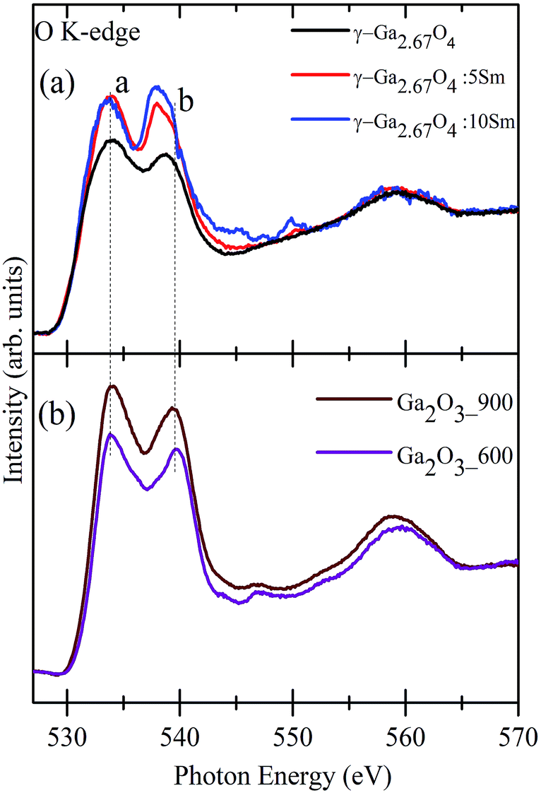 | ||
| Fig. 2 (a) Normalized O K-edge XANES of (a) γ-Ga2.67O4, γ-Ga2.67O4:5Sm and γ-Ga2.67O4:10Sm samples and (b) O K-edge spectra of Ga2O3_600 and Ga2O3_900 samples. Dotted vertical lines on the peaks a and b indicate the energy position. | ||
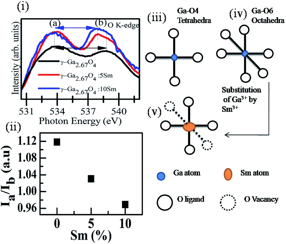 | ||
| Fig. 3 (i) Magnified view of peaks a and b in the O K-edge spectra of pure and Sm doped γ-Ga2.67O4. (ii) Shows the intensity ratio (Ia/Ib) variation as a function of Sm concentration calculated from the O K-edge XANES of pure and Sm doped γ-Ga2.67O4 samples. (iii) Shows a schematic of Ga-O4 tetrahedra with four oxygen ligands surrounding the Ga atom. (iv) Shows the schematic of Ga-O6 octahedra with six oxygen ligands surrounding the Ga atom. (v) Shows a schematic of Sm substitution at the Ga sites and the formation of O vacancies due to the lattice disorders and strain. | ||
By considering the Δ0 of the samples, we expect that the fractional occupancy of Ga atoms at tetrahedral sites is larger in the case of γ-Ga2.67O4 polymorphs and the octahedral sites are the favourable sites of Ga atoms in the β phasic samples. In a previous study, the preferred octahedral sites occupancy for the dopants were reported in spinel phase MnFe2O4 nanoparticles.50
Here, we may hypothesize that the Sm doping in the γ-Ga2.67O4 lattice offers more tetrahedral sites to the metal atoms at the expense of octahedral sites. Under the condition of substitutional doping of Sm at the Ga sites, if we assume that isovalent Sm3+ ions take the octahedral sites of Ga3+ ions, O vacancies are expected to form because of the disorder/strain produced via imbalance of ionic radii and electronegativity of Sm3+ and Ga3+ ions. Formation of O vacancies has also been reported in the isovalent (i.e., Sn4+, Hf4+ and Zr4+) element doped CeO2 nanoparticles (Ce4+ ions in CeO2), and was ascribed to the imbalance of ionic radii and lattice distortion.32,33,51 In the case of Ga-O4 tetrahedra, there are only four O ligand approaches to the Ga atoms (see the schematic in Fig. 3(iii)). Similarly, six O ligands form Ga-O6 octahedra with the Ga atoms (see the schematic in Fig. 3(iv)). Reduction of metal-O6 octahedra into metal-O4 tetrahedra is possible via O vacancy formation and is shown in the Fig. 3(v). Further analysis at Ga K-edge XANES and EXAFS is helpful to elaborate such a hypothesis of an increase in the metal-O4 tetrahedral sites and decrease in the metal-O6 octahedral sites in the Sm doped γ-Ga2.67O4 and is discussed in the following sections.
The Ga K-edge XANES originates from the 1s → 4p transitions and can be used for understanding the inconsequential local electronic structure differences among the polymorphous Ga2O3 compounds.48,49,52–54 Fig. 4(a) shows the Ga K-edge XANES spectra of γ-Ga2.67O4, γ-Ga2.67O4:5Sm and γ-Ga2.67O4:10Sm samples while Fig. 4(c) shows the second derivates of the Ga K-edge XANES spectra. Here, we have analysed the Ga K-edge XANES spectra by concerning the two aspects; (i) valence state change of Ga3+ ions and (ii) perturbation in the Ga lattice site occupancy (i.e., change in the Ga-O6 octahedra and Ga-O4 tetrahedra proportions), if any, upon Sm doping or annealing conditions. The edge-energy position and other spectral features of the pure and Sm doped γ-Ga2.67O4 samples fairly match each other (can be seen in the second derivate spectra) and nullify any valence state change upon Sm doping. Similar to the Ga K-edge XANES, the Sm L-edge XANES spectra and second derivate spectra of the γ-Ga2.67O4:5Sm and γ-Ga2.67O4:10Sm samples do not show any noteworthy changes and, thus, the possibility of valence state change of Sm ions can be neglected. The Ga K-edge and Sm L-edge XANES results were further cross-checked with the Ga L-edge and Sm M5,4-edge XANES and convey the +3 valence state of Ga and Sm ions (see Fig. S3 and S4 in the ESI† and discussion therein). Sm L-edge and Sm M-edge XANES are convincing of Sm3+ ions in the samples but the existence of Sm at the surface/grain boundaries of NPs may not be explained within the periphery of the XANES results. Interesting spectral changes were observed in the Ga K-edge XANES spectra, while we have analysed the white-line region of γ-Ga2.67O4 and Ga2O3_900 samples, by normalizing the white-line peak intensity (see the inset of Fig. 4(a)). It is evidenced from the figure that the Ga2O3_900 sample (i.e., β-Ga2O3 phase) exhibits a broad white line peak compared with the sharp peak in γ-Ga2.67O4. It seems that the white-line peak position of the β-Ga2O3 sample is at a slightly higher energy (∼2.2 eV) compared with the γ-Ga2.67O4 sample. It is known for the transition metal compounds that the edge-energy and white-line peak position progressively shift towards a higher energy with increasing valence state (cation charge) of metal ions.55 In the present study, the edge-energy positions are nearly identical; however, the white line peak positions give the impression of positive energy shifting for the β-Ga2O3 compound with respect to γ-Ga2.67O4. In a previous report, the Al K-edge XANES also showed white-line peak shifting towards a higher energy with an increase of the oxygen coordination number of Al from 4 to 6 (i.e., sodalite to kyanite transformation).56 Similarly, a Ga K-edge XANES spectrum of α-Ga2O3 has been reported with a +2 eV shifting in the white-line peak position with respect to GaAs despite the same valence state of the Ga ions (i.e., Ga3+) in both of the compounds.52 The existence of a higher energy white-line peak in α-Ga2O3 and a lower energy white-line peak in GaAs was ascribed to the diverse site occupancy of Ga atoms.48,52 In the GaAs compound, the Ga atoms occupy regular tetrahedral sites, whereas in α-Ga2O3 the Ga atoms are in distorted octahedral sites.52 By considering the previous reports and findings of our Ga K-edge XANES, the low energy white-line peak in the present study of γ-Ga2.67O4 sample can be anticipated as a favourable tetrahedral occupancy of Ga atoms, whereas the broadened or positive energy shifted white-line peak in the Ga2O3_900 sample may be an indication of mixed occupancy of the Ga atoms at tetrahedral and octahedral sites.
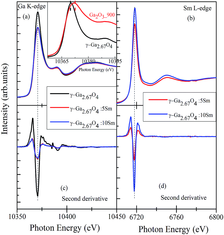 | ||
| Fig. 4 (a) and (b) show the Ga K-edge and Sm L3-edge XANES spectra, respectively. The lower panels (c) and (d) are the second derivative spectra of the Ga K-edge and Sm L-edge, respectively. Inset of (a) shows a comparison of the white-line peaks of the γ-Ga2.67O4 and Ga2O3_900 samples. | ||
To understand the quantitative Ga occupancy in Ga2O3_900, γ-Ga2.67O4, and Sm doped γ-Ga2.67O4, we have deconvoluted the white line peak of Ga K-edge XANES and present it in Fig. 5(a–d). The deconvolution was done by assuming the two components in the main peak region (i.e., 10355 eV to 10385 eV) and the fittings were done by applying the Gaussian curve fitting method.48,49 The details of the fitting procedure and the other parameters like peak energy, full width at half maxima of the peaks and the fractional percentages of tetrahedral and octahedral Ga atoms (i.e., Ga(t)% and Ga(o)%) in various samples are provided in Table S1 of the ESI.† According to previous reports,48,49,52 the Gaussian 1 (magenta colour) and Gaussian 2 (olive colour) in Fig. 5 can be regarded as the contribution from the tetrahedral (Ga(t)) and octahedral (Ga(o)) occupancy of Ga atoms, respectively. The integrated areas of Gaussian 1 and Gaussian 2 have been applied to determine the fractional percentage of Ga(t) and Ga(o) from various samples. Detailed calculations are provided in the ESI.† Our calculations convey that the Ga2O3_900 sample exhibits 48.4% and 51.6% of Ga(t) and Ga(o) atoms, respectively (i.e., Ga(t)/Ga(o) ratio of ∼0.92). In previous studies, a 1:1 ratio of Ga(t):Ga(o) has been reported for the commercial β-Ga2O3 compound.48,49 A slightly smaller Ga(t):Ga(o) ratio from the Ga2O3_900 sample may be due to the higher occupancy of Ga atoms on octahedral sites. On the other hand, the γ-Ga2.67O4 sample has shown 58.8% and 41.2% fractional percentages of Ga(t) and Ga(o), respectively (i.e., Ga(t)/Ga(o) ratio of ∼1.4). Ga(t)/Ga(o) ratios were further increased for the γ-Ga2.67O4:5Sm (∼1.51) and γ-Ga2.67O4:10Sm (∼1.62) samples. The highest Ga(t)/Ga(o) ratio was reported to be ∼1.8 for the poorly crystalline and small sized Ga2O3 samples48 and is in agreement with our results. Ga K-edge XANES results imply that the γ phasic samples have preferred tetrahedral sites of Ga species and the substitution of Sm leads to much octahedral site deformation. Population of Ga atoms at tetrahedral (Ga-O4) sites at the expense of octahedral (Ga-O6) sites may facilitate O ion vacancy in the γ-Ga2.67O4 lattice leading to more unoccupied O 2p hybridized orbitals in the Sm doped samples, as illustrated in the O K-edge XANES. The smaller Δ0 in the O K-edge spectra is analogous to the higher Ga(t):Ga(o) ratio for the pure and Sm doped samples and is convincing of the higher metal-O4 tetrahedra in the γ-Ga2.67O4, γ-Ga2.67O4:5Sm and γ-Ga2.67O4:10Sm samples, compared with β-Ga2O3.
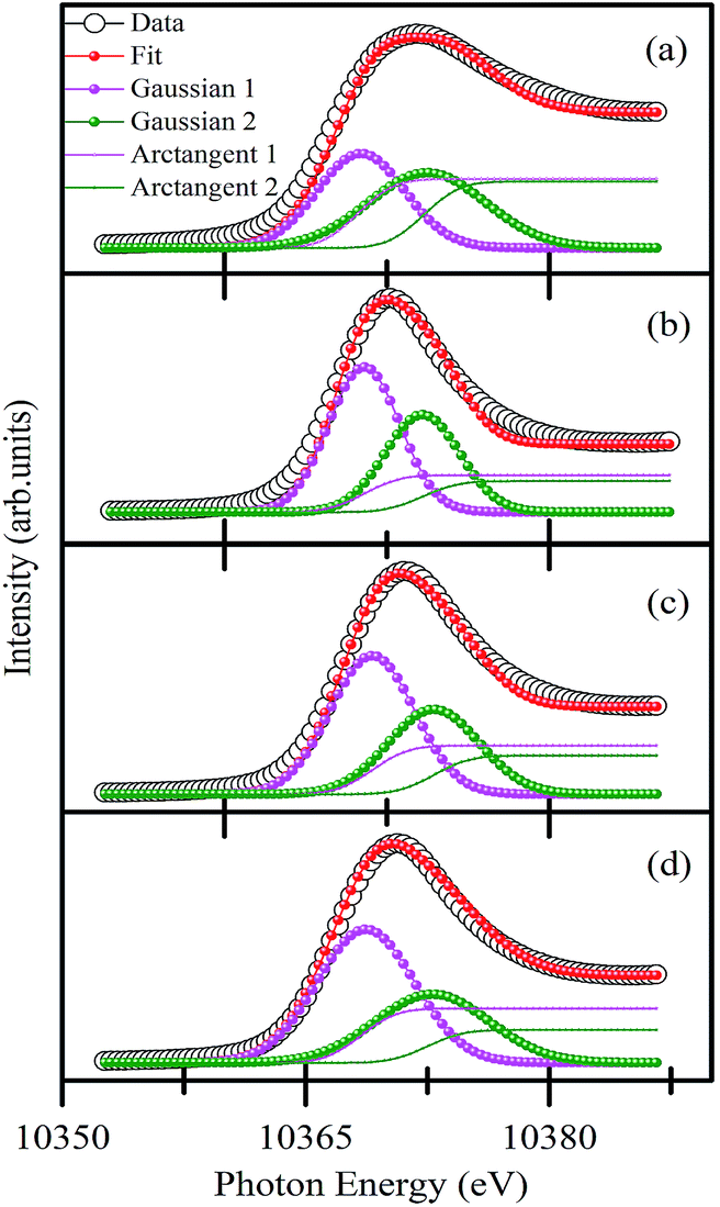 | ||
| Fig. 5 Deconvolution of the Ga K-edge white line peak of (a) Ga2O3_900, (b) γ-Ga2.67O4, (c) γ-Ga2.67O4:5Sm and (d) γ-Ga2.67O4:10Sm samples. Gaussian 1 and Gaussian 2 represent the tetrahedral and octahedral contributions, respectively. Arctangent 1 and arctangent 2, which were assigned for the continuum absorption, correspond to Gaussian 1 and Gaussian 2, respectively. The energy of the inflection point of the arctangent curve is taken to be the same as that of the corresponding Gaussian curve. | ||
EXAFS study at Ga K-edge
In order to get a further understanding of the local structure differences among the pure γ-Ga2.67O4, β-Ga2O3 and Sm doped γ-Ga2.67O4 samples, systematic Ga K-edge EXAFS data are investigated by applying the ATHENA-ARTEMIS and FEFF calculations.57,58 Details of the EXAFS data simulations are provided in the ESI.† The spectra presented in the Fig. 6 are not corrected for phase shift; however, phase-corrected spectra are provided in the ESI.† The χ(R) vs. R spectrum of Ga2O3_900 sample shows a distinct doublet in the first oscillation of the Ga–O shell; however, the pure and Sm doped γ-Ga2.67O4 samples are likely to have one oscillation in the Ga–O shell. During the simulations, individual oscillations from the tetrahedrally coordinated Ga and octahedrally coordinated Ga were examined and exhibit bond lengths of ∼1.85 Å and ∼1.99 Å for the Ga–O shells of the tetrahedral and octahedral coordinated Ga atoms, respectively. Similarly, a sharp oscillation at 3.0 Å and a mild oscillation at 3.3 Å were also observed due to the octahedral and tetrahedral Ga–Ga shells, respectively. The appearance of such features in the Ga2O3_900 sample is characteristic of the β-Ga2O3 phase and is due to contributions from the tetrahedrally and octahedrally coordinated Ga atoms in this sample.48,49 After accreting the contributions from both of the individual oscillations from tetrahedrally and octahedrally coordinated Ga, the experimental spectra were fairly simulated for the Ga2O3_900 sample (see Fig. 6(a) and (e)). The simulated structural parameters (see Table 1) show that there are two Ga–O bond distances (i.e., 1.82 Å and 1.92 Å) for the tetrahedral and octahedral occupation of Ga, respectively. In previous reports, the average Ga–O bond distance for the β-Ga2O3 phase is reported to be 1.83 Å for the tetrahedrally coordinated Ga atoms and 2.0 Å for the octahedrally coordinated Ga atoms.48,49 Our simulated results for the Ga2O3_900 sample are in fair agreement with the previously reported EXAFS results for β-Ga2O3, thus confirming our XRD and Raman results on the formation of a β-Ga2O3 phase in this sample.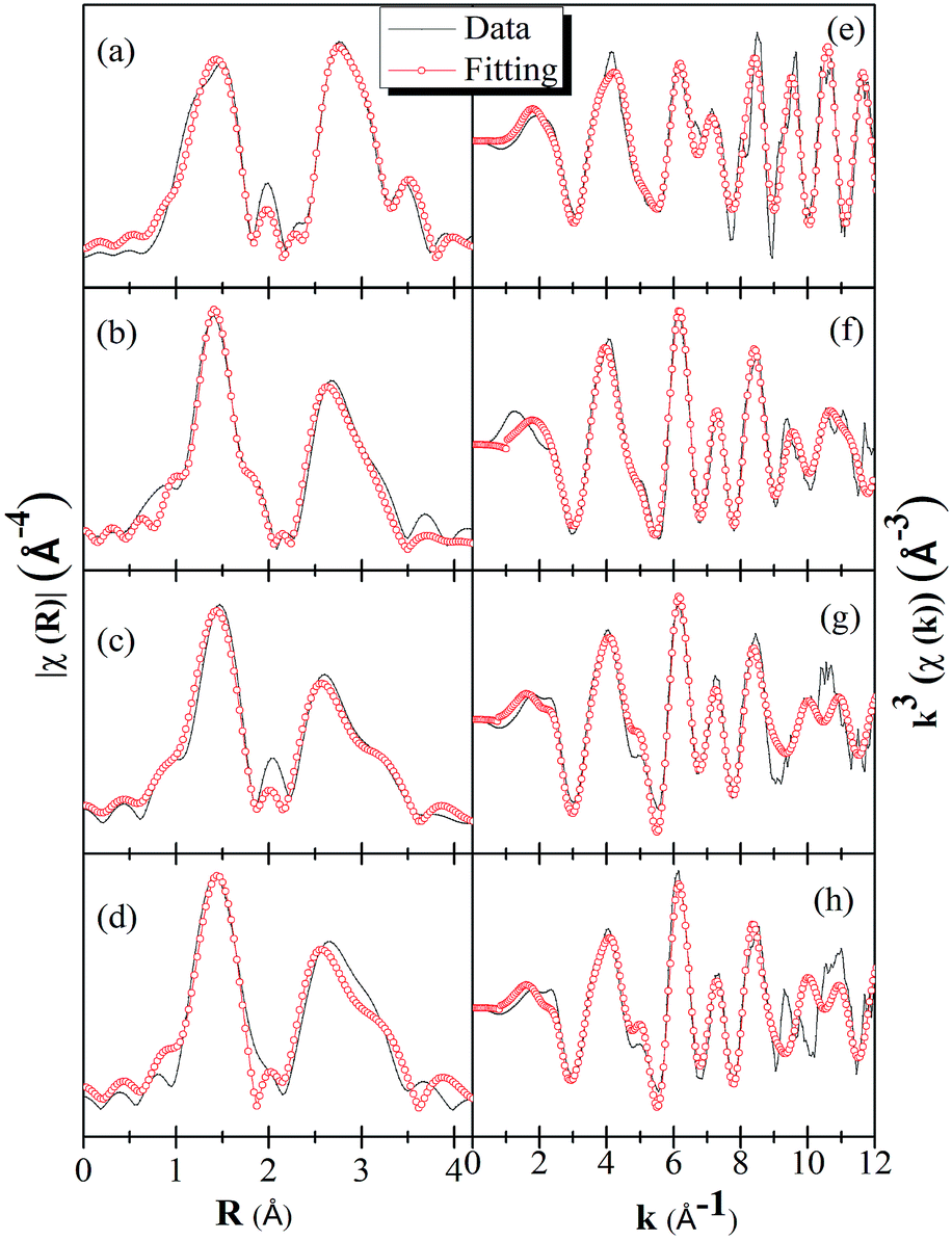 | ||
| Fig. 6 χ(R) vs. R spectra of (a) Ga2O3_900, (b) γ-Ga2.67O4, (c) γ-Ga2.67O4:5Sm and (d) γ-Ga2.67O4:10Sm, respectively. χ(k) vs. k spectra of (e) Ga2O3_900, (f) γ-Ga2.67O4, (g) γ-Ga2.67O4:5Sm and (h) γ-Ga2.67O4:10Sm, respectively. The spectra are not corrected for phase shift. | ||
| Name | Ga sites | Shell | N | R (Å) | σ2 (Å2) | E0 (eV) | Ga(t)/Ga(o) |
|---|---|---|---|---|---|---|---|
| Ga2O3_900 | Gao | Ga–O | 5.4 | 1.92(3) | 0.012(2) | 3.0 | 0.85 |
| Ga–Ga | 5.4 | 3.09(3) | 0.009(5) | ||||
| Gat | Ga–O | 3.0 | 1.82(7) | 0.047(0) | |||
| Ga–Ga | 6.1 | 3.34(7) | 0.008(0) | ||||
| γ-Ga2O3 | Gao | Ga–O | 4.1 | 2.01(7) | 0.026(4) | 2.5 | 1.17 |
| Ga–Ga | 4.7 | 2.97(1) | 0.007(4) | ||||
| Gat | Ga–O | 3.2 | 1.85(0) | 0.002(0) | |||
| Ga–Ga | 5.7 | 3.34(2) | 0.012(4) | ||||
| γ-Ga2O3:5Sm |
Gao | Ga–O | 3.7 | 2.04(9) | 0.011(8) | 2.2 | 1.37 |
| Ga–Ga | 3.9 | 3.01(4) | 0.008(9) | ||||
| Gat | Ga–O | 3.4 | 1.90(8) | 0.007(1) | |||
| Ga–Ga | 5.1 | 3.45(0) | 0.047(0) | ||||
| γ-Ga2O3:10Sm |
Gao | Ga–O | 3.5 | 2.06(9) | 0.038(5) | 2.7 | 1.59 |
| Ga–Ga | 3.5 | 3.11(3) | 0.007(0) | ||||
| Gat | Ga–O | 3.3 | 1.92(7) | 0.004(8) | |||
| Ga–Ga | 4.5 | 3.46(9) | 0.018(8) |
It is also noticeable from Fig. 6(b) that the intensity of the Ga–Ga shell (between the 2–3.4 Å) is quite smaller than that of the Ga–O shell intensity, while it was quite comparable with that of the Ga2O3_900 sample. This is due to the fact that the Ga2O3_900 sample has a high crystallinity and larger particle size compared with the γ-Ga2.67O4 sample. Diminishing the Ga–Ga shell intensity in Fig. 6(c and d), for the γ-Ga2.67O4:Sm samples, could be related to the net decrease in the nanoparticle size and increase in the amorphous content in the samples. In previous reports, a continuous decrease in the EXAFS oscillations with a decrease in the nanoparticle size is also reported.59 It is noticeable from Table 1 that the Ga–O and Ga–Ga bond distances are longer for the Sm doped sample compared with pure Ga2.67O4. The net increase in the Ga–O or Ga–Ga bond distances is, certainly, due to the structural perturbation in the crystalline lattice of gallium oxide upon Sm3+ ion doping. In the XRD studies, we have noticed an enlargement of d(311) values for the Sm3+ ion doped samples. Thus, the enlarged Ga–O and Ga–Ga bond distances are the consequences of the insertion of larger Sm3+ ions at the lattice position of Ga3+ ions. In previous reports,48,49 Ga–O shell coordination numbers were applied to calculate the fractional Ga(t) and Ga(o). We have also evaluated the Ga(t)/Ga(o) = (N/4)/(N/6) ratio from the coordination number of Ga–O shell.48 It is noticeable from Table 1 that the Ga(t)/Ga(o) ratios, for all of the samples, are nearly the same as obtained from the Ga K-edge XANES. In the previous EXAFS analysis,48 the maximum Ga(t)/Ga(o) ratio was evaluated to be ∼1.7 for the poorly crystalline and small sized (2–6 nm) Ga2O3 NP samples and is in accordance with our findings. Our XANES and EXAFS results are, thus, convincing of favourable tetrahedral sites of the Ga atoms in γ-Ga2.67O4 which are further increased in the Sm doped samples leading to higher Ga(t)/Ga(o) ratios.
Photoluminescence study
Ga2O3 is known as the widest band gap material (Eg ≈ 4.8 eV) among all of the known transparent conducting oxides. Its semiconducting nature originates from the shallow donor states caused by native defects.18–23 The photoluminescence from this compound is also a matter of debate and has been understood on the basis of donor–acceptor pair (DAP) recombination.60–62 Yet, the exact nature of the localized donor and acceptor sites is under investigation. It is considered that the acceptor is a gallium–oxygen vacancy pair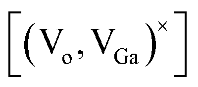 and the donor is an oxygen vacancy
 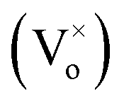 . After illuminating the Ga2O3 with sufficient energy of photons, an electron with the donor and a hole with the acceptor level can be generated with a blue-green emission; however, particle size dependence60 can be achieved according to the relation,61
 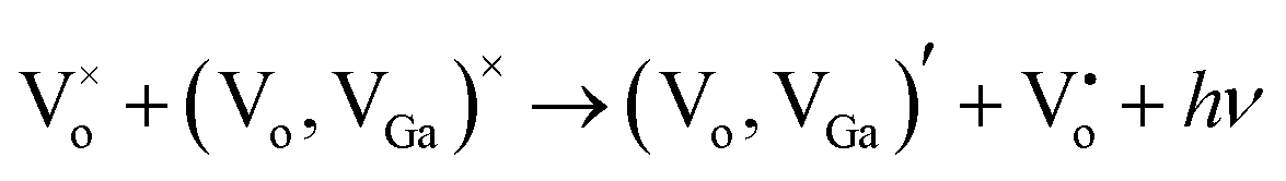 . Fig. 7 shows the room temperature PL spectrum of (a) γ-Ga2.67O4, (b) γ-Ga2.67O4:5Sm (c) γ-Ga2.67O4:10Sm, (d) Ga2O3_600 and (e) Ga2O3_900 samples. In the previous reports, an intense blue emission has been reported from the γ-Ga2O3 colloidal nanoparticles.60,61 In the present study, the γ-Ga2.67O4 nanoparticles exhibit a dominating emission centred at ∼520 nm (cyan-green) with a significant band at ∼434 nm (violet-blue emission). This may be due to the fact that γ-Ga2.67O4 nanoparticles contain a lower concentration of Ga and O vacancy sites, compared with the previously reported Ga2O3 colloidal nanoparticles, providing a lower number of DAPs (attributed to the lower PL intensity of the violet-blue band) and a larger average energy separation between the recombining pairs or lower Coulomb interaction between the donor and acceptor sites (attributed to cyan-green PL).
 | ||
| Fig. 7 Room temperature PL spectra of (a) pure γ-Ga2.67O4, (b) γ-Ga2.67O4:5Sm, (c) γ-Ga2.67O4:10Sm, (d) Ga2O3_600 and (e) Ga2O3_900 samples. | ||
While comparing the PL spectra of γ-Ga2.67O4 nanoparticles and the annealed samples (Ga2O3_600 and Ga2O3_900), it is noticeable that the annealed samples show a dominating green emission at ∼548 nm and a negligible blue emission band. The red shift in the PL spectra, comparing with pure γ-Ga2.67O4, indicates a smaller average energy separation between the recombining pairs in the annealed samples. The annealing induced ripening and fusion of particles, as evidenced in the TEM study, may have hidden the surface defect induced shallow energy levels in the energy gap of the material, leading to the quenching of the blue emission from the Ga2O3_600 and Ga2O3_900 samples. Only the interior defects  , which have a smaller energy separation of donor–acceptor pairs or more Coulomb interactions, are expected to be responsible for the green emission from the Ga2O3_600 and Ga2O3_900 samples. An interesting variation can be seen in the PL spectra of Sm doped samples: (i) a low-intensity band evolves in the deep violet region (∼396 nm), (ii) the intensity of the ∼434 nm band is increased and (iii) intense bands appear between 550 nm and 675 nm. Taken together, XRD, XAS and PL data indicate that Sm doping in γ-Ga2.67O4 nanoparticles causes a change in DAP recombination because of several factors: (i) a decrease in the average particle size, which provides more surface related defect states,63 (ii) alteration in the Ga and O local lattice site occupancy, which gives diverse defect levels in the compound18–20 and (iii) the existence of the Sm3+ ion in the γ-Ga2.67O4 lattice, which provides distinct defect states and intra-4f transitions.64,65 The broad range of luminescence from the γ-Ga2.67O4:Sm nanoparticles can be understood by knowing the energy and charge transfer process in distinct electronic states.
In Fig. 8, we present a schematic of the DAP and Sm3+ ion transition induced luminescence in the γ-Ga2.67O4:Sm nanoparticles. Excitation by the 325 nm wavelength from a He–Cd laser leads to electronic transitions and trapping of photo excited electrons and holes in the donor and acceptor states, respectively. Recombination of electrons and holes leads to typical emission spectra from γ-Ga2.67O4 nanoparticles. The energy (or colour) of emitted radiation is governed by the coulombic interaction between the charge donor and acceptors and can be expressed as;60–62 E = Eg − (Edonor + Eacceptor) + Ecoulombic ± nEphonon. Here, Eg is the band gap energy of the material, Edonor and Eacceptor are the donor and acceptor binding energies, respectively. The Ephonon term represents the energies of phonons involved in the radiative transitions and the coulombic interaction term (Ecoulombic = e2/4πεr) is the deciding term for the emitted energy (or colour) from a DAP transition. Since the average donor–acceptor separation (r) becomes narrower for the smaller sized particles,60–62 a higher emission energy can be expected from the above relation for a smaller sized particle. The observed violet emission (∼395.5 nm) and increased intensity of the ∼434 nm band in the Sm doped samples may be the consequence of an Sm doping induced decrease of particle size and increase in the defect concentration. Our O K-edge and Ga K-edge XANES/EXAFS are convincing of O and Ga defect formation and Ga lattice site occupancy alteration upon the insertion of Sm3+ ions. These kinds of defect states are certainly responsible for the intensification of the ∼434 nm band.
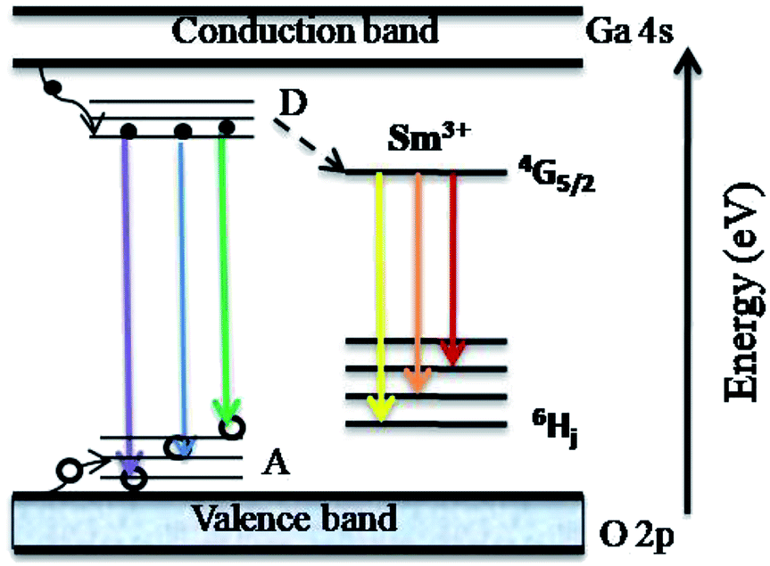 | ||
| Fig. 8 Schematic representation of the charge and energy transfer processes involved in the luminescence characteristics of Sm3+ doped γ-Ga2.67O4 nanoparticles. The solid spheres and open circles represent electrons and holes, respectively. D and A correspond to the defect induced formation of donor and acceptor bands, respectively. | ||
Donor and acceptor states not only provide DAP induced radiative transitions but also play a role in the sensitization of the Sm emission by nonradiative transfer of the DAP exciton energy to the doped rare earth ions (shown by a dashed black line in Fig. 8).12 The 4f electrons of rare-earth ions in the host materials are quite similar to the free ions and the emission characteristics are determined by the crystalline fields of the host compound around the rare-earth ions.12,64 In several reports, the 3+ valence state of rare-earth ions was reduced to 2+, even under in situ XAS data collection, leading to intriguing electronic structure and luminescence properties.12,65 In the present study, our Sm L-edge and Sm M5,4-edge XANES, along with the multiplet calculations, have confirmed Sm3+ ions in the samples, and therefore Sm3+ reduction into Sm2+ can be neglected and the observed luminescence properties are the consequences of defect formation and the Sm3+ ion related 4G5/2 → 6Hj transition induced emission properties. Despite the enhancement in the defect induced luminescence bands (violet-blue-green bands) the intensity of the Sm3+ ions induced transitions,64,65 4G5/2 → 6H5/6 (yellow emission), 4G5/2 → 6H7/6 (orange emission) and 4G5/2 → 6H9/6 (red emission), are also enhanced, conveying that the luminescence properties of γ-Ga2.67O4 can be engineered by the formation of controlled defect states and incorporation of variable Sm3+ ion concentration. The photoluminescence spectra of the samples were converted to the Commission International de I'Eclairage (CIE-1913) chromaticity diagram and are presented in the Fig. 9. It is visible from the CIE colour chromaticity diagram that the pure γ-Ga2.67O4 nanoparticle sample exhibits DAP induced cyan-green emission characteristics (CIE coordinates, 0.26, 0.43) while the Ga2O3_600 (CIE coordinates, 0.36, 0.45) or Ga2O3_900 (CIE coordinates, 0.37, 0.46) samples exhibits green yellow emission which is analogous to the previous reports where the increase of particle size had demonstrated the red-shifted PL bands.60,61 By considering the standard CIE coordinates for the white light (i.e., 0.333, 0.333),66 we can state that the Sm doped γ-Ga2.67O4 nanoparticles have shown a nearly white line emission, i.e., ranging from violet-blue to orange-red emission. The CIE coordinates for the γ-Ga2.67O4:5Sm and γ-Ga2.67O4:10Sm samples are (0.28, 0.34) and (0.30, 0.35), respectively.
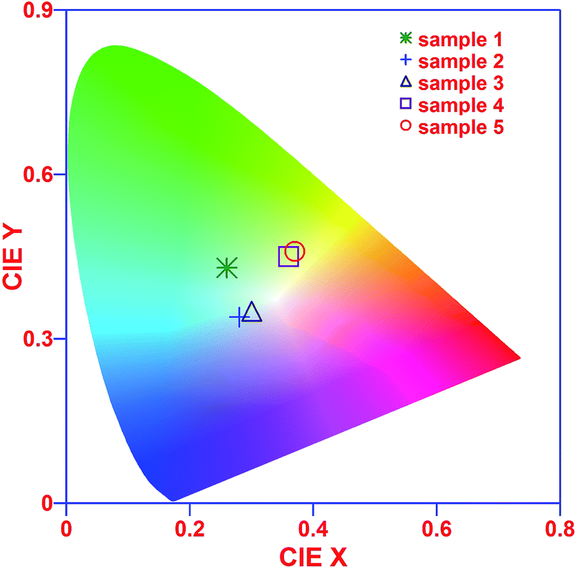 | ||
| Fig. 9 CIE colour chromaticity diagram of sample 1 (pure γ-Ga2.67O4), sample 2 (γ-Ga2.67O4:5Sm), sample 3 (γ-Ga2.67O4:10Sm), sample 4 (Ga2O3_600) and sample 5 (Ga2O3_900). | ||
Conclusions
Specifically, the non-aqueous synthesis with hydrazine monohydrate has helped us to fabricate the barely reported and metastable γ-Ga2.67O4 nanoparticles in the present study. XRD and Raman results are convincing of the single phase nature of the as-prepared and annealed samples. XRD and TEM studies signify a particle size reduction and poor crystallinity in the Sm doped samples. Ga K/L-edge and Sm L3/M5,4-edge XANES have confirmed Ga3+ and Sm3+ ions in the samples and have also ruled out the valence reduction of metal ions under the Sm doping and annealing conditions. O K-edge XANES has shown a systematic increase in the intensity of O 2p and Ga 4s/4p hybridized orbitals and decrease in the crystal field splitting energy upon increasing the Sm concentration in the γ-Ga2.67O4 lattice. Detailed analysis at the Ga K-edge XANES and EXAFS data has conveyed a ∼0.9 Ga(t)/Ga(o) ratio in the β-Ga2O3 phase, signifying a higher proportion of Ga-O6 octahedra. Pure γ-Ga2.67O4 and Sm doped γ-Ga2.67O4 samples have exhibited higher Ga(t)/Ga(o) ratios and signify the higher Ga-O4 tetrahedra proportions. Photoluminescence spectra and CIE diagrams have shown that the γ-Ga2.67O4 phase has exhibited DAP induced cyan-green emission. The Sm incorporation into the γ-Ga2.67O4 lattice has offered a wide range of emission, with CIE coordinates closer to that of white light, ranging from violet-blue to orange-red. The results of this research work provide a guideline for the preparation and understanding of the metastable phase of gallium oxide, which is not only interesting for its local atomic/electronic structure properties but also exhibits a wide range of emission characteristics upon Sm doping.Conflicts of interest
There are no conflicts to declare.Acknowledgements
This work was supported by Korea Institute of Science and Technology, Seoul, Korea (KIST Project nos. 2V04081 and 2V04611). H. J. Shin and A. Sharma would like to acknowledge support by the Basic Science Research Program (NRF-2015R1A5A1009962) through the National Research Foundation of Korea funded by the Korea government Ministry of Science, ICT & Future Planning. Authors are also thankful to Dr Jitendra Pal Singh (KIST-PAL beam line at Pohang Accelerator Laboratory, South Korea) and Dr Ankush Vij (Department of Physics, Amity University, Gurgaon, India) for fruitful discussion on EXAFS and PL data analysis.Notes and references
- R. Roy, V. G. Hill and E. F. Osborn, J. Am. Chem. Soc., 1952, 74, 719 CrossRef CAS.
- S. Yoshioka, H. Hayashi, A. Kuwabara, F. Oba, K. Matsunaga and I. Tanaka, J. Phys.: Condens. Matter, 2007, 19, 346211 CrossRef.
- H. Y. Playford, A. C. Hannon, E. R. Barney and R. I. Walton, Chem.–Eur. J., 2013, 19, 2803 CrossRef CAS PubMed.
- H. Y. Playford, A. C. Hannon, M. G. Tucker, D. M. Dawson, S. E. Ashbrook, R. J. Kastiban, J. Sloan and R. I. Wolton, J. Phys. Chem. C, 2014, 118, 16188 CAS.
- M. Passlack, E. F. Schubert, W. S. Hobson, M. Hong, N. Moriya, S. N. G. Chu, K. Konstadinidis, J. P. Mannaerts, M. L. Schnoes and G. J. Zydzik, J. Appl. Phys., 1995, 77, 686 CrossRef CAS.
- L. Mazeina, F. Keith Perkins, V. M. Bermudez, S. P. Arnold and S. M. Prokes, Langmuir, 2010, 26, 13722 CrossRef CAS PubMed.
- D. Fracasso, M. I. Muglali, M. Rohwerder, A. Terfort and R. C. Chiechi, J. Phys. Chem. C, 2013, 117, 11367 CAS.
- V. Ghodsi, S. Jin, J. C. Byers, Y. Pan and P. V. Radovanovic, J. Phys. Chem. C, 2017, 121, 9433 CAS.
- X. S. Wang, J. Q. Situ, X. Y. Ying, H. Chen, H. F. Pan, Y. Jin and Y. Z. Du, Acta Biomater., 2015, 22, 164 CrossRef CAS PubMed.
- R. Lorenzi, A. Paleari, N. V. Golubev, E. S. Ignateva, V. N. Sigaev, M. Niederberger and A. Lauria, J. Mater. Chem. C, 2015, 3, 41 RSC.
- T. Wang and P. V. Radovanovic, J. Phys. Chem. C, 2011, 115, 18473 CAS.
- A. Layek, B. Yildirim, V. Ghodsi, L. N. Hutfluss, M. Hegde, T. Wang and P. V. Radovanovic, Chem. Mater., 2015, 27, 6030 CrossRef CAS.
- H. He, R. Orlando, M. A. Blanco and R. Pandey, Phys. Rev. B, 2006, 74, 195123 CrossRef.
- M. Mohamed, C. Janowitz, I. Unger, R. Manzke, Z. Galazka, R. Uecker, R. Fornari, J. R. Weber, J. B. Varley and C. G. Van de Walle, Appl. Phys. Lett., 2010, 97, 211903 CrossRef.
- Y. Jinliang and Q. Chong, J. Semicond., 2016, 37, 042002 CrossRef.
- N. T. Son, K. Goto, K. Nomura, Q. T. Thieu, R. Togashi, H. Murakami, Y. Kumagai, A. Kuramata, M. Higashiwaki, A. Koukitu, S. Yamakoshi, B. Monemar and E. Janzén, J. Appl. Phys., 2016, 120, 235703 CrossRef.
- X. Qiu, J. Zhang, H. Dong and X. Zhou, Theor. Chem. Acc., 2017, 136, 79 CrossRef.
- S. Ye, Y. Zhang, H. He, J. Qiu and G. Dong, J. Mater. Chem. C, 2015, 3, 2886 RSC.
- C. C. Huang and C. S. Yeh, New J. Chem., 2010, 34, 103 RSC.
- B. K. Kang, S. R. Mang, D. H. Go and D. H. Yoon, Mater. Lett., 2013, 111, 67 CrossRef CAS.
- E. I. EL-Sayed, A. A. Al-Ghamdi, S. Al-Heniti, F. Al-Marzouki and F. El-Tantawy, Mater. Lett., 2011, 65, 317 CrossRef CAS.
- C. T. Shao, W. Z. Lang, X. Yan and Y. J. Guo, RSC Adv., 2017, 7, 4710 RSC.
- K. Shimura and H. Yoshida, Phys. Chem. Chem. Phys., 2012, 14, 2678–2684 RSC.
- D. Chiche, M. Digne, R. Revel, C. Chanéac and J. P. Jolivet, J. Phys. Chem. C, 2008, 112, 8524 CAS.
- A. Sharma, M. Varshney, K. H. Chae, H. J. Shin and S. O. Won, Curr. Appl. Phys., 2016, 16, 1326 CrossRef.
- L. M. Moreau, D. H. Ha, H. Zhang, R. Hovden, D. A. Muller and R. D. Robinson, Chem. Mater., 2013, 25, 2394 CrossRef CAS.
- P. Thakur, R. Kumar, J. C. Cezar, N. B. Brookes, A. Sharma, S. K. Arora, S. Gautam, A. Kumar, K. H. Chae and I. V. Shvets, Chem. Phys. Lett., 2011, 501, 404 CrossRef CAS.
- S. Gautam, S. N. Kane, B. G. Park, J. Y. Kim, L. K. Varga, J. H. Song and K. H. Chae, J. Non-Cryst. Solids, 2011, 357, 2228 CrossRef CAS.
- A. Lussier, J. Dvorak, Y. U. Idzerda, S. B. Ogale, S. R. Shinde, R. J. Choudary and T. Venkatesan, J. Appl. Phys., 2004, 95, 7190 CrossRef CAS.
- A. Sharma, A. P. Singh, P. Thakur, N. B. Brookes, S. Kumar, C. G. Lee, R. J. Choudhary, K. D. Verma and R. Kumar, J. Appl. Phys., 2010, 107, 093918 CrossRef.
- W. C. Wang, S. Y. Chen, P. A. Glans, J. Guo, R. Chen, K. W. Fong, C. L. Chen, A. Gloter, C. Lin Chang, T. S. Chan, J. M. Chen, J. F. Leed and C. L. Dong, Phys. Chem. Chem. Phys., 2013, 15, 14701–14707 RSC.
- A. Sharma, M. Varshney, H. J. Shin, Y. J. Park, M. G. Kim, T. K. Ha, K. H. Chae and S. Gautam, Phys. Chem. Chem. Phys., 2014, 16, 19909 RSC.
- A. Sharma, M. Varshney, J. H. Park, T. K. Ha, K. H. Chae and H. J. Shin, Phys. Chem. Chem. Phys., 2015, 17, 30065 RSC.
- X. Tan, T. Yao, R. Long, Z. Sun, Y. Feng, H. Cheng, X. Yuan, W. Zhang, Q. Liu, C. Wu, Y. Xie and S. Wei, Sci. Rep., 2012, 2, 466 CrossRef PubMed.
- A. Sharma, M. Varshney, H. J. Shin, K. H. Chae and S. O. Won, Spectrochim. Acta, Part A, 2017, 173, 549 CrossRef CAS PubMed.
- Y. Wu, L. Fan, W. Huang, S. Chen, S. Chen, F. Chen, C. Zou and Z. Wu, Phys. Chem. Chem. Phys., 2014, 16, 17705 RSC.
- A. Sharma, M. Varshney, W. C. Lim, H. J. Shin, J. P. Singh, S. O. Won and K. H. Chae, Phys. Chem. Chem. Phys., 2017, 19, 6397 RSC.
- A. I. Frenke, Chem. Soc. Rev., 2012, 41, 8163 RSC.
- Z. Sun, W. Yan, T. Yao, Q. Liu, Y. Xie and S. Wei, Dalton Trans., 2013, 42, 13779 RSC.
- M. Newville, Rev. Mineral. Geochem., 2014, 78, 33 CrossRef CAS.
- M. Varshney, A. Sharma, H. J. Shin, H. H. Lee, T. Y. Jeon, B. H. Lee, K. H. Chae and S. O. Won, J. Phys. Chem. Solids, 2017, 110, 187 CrossRef CAS.
- B. Choudhury and A. Choudhury, Curr. Appl. Phys., 2013, 13, 217 CrossRef.
- J. G. Chen, Surf. Sci. Rep., 1997, 30, 1–152 CrossRef CAS.
- X. T. Zhou, F. Heigl, J. Y. P. Ko, M. W. Murphy, J. G. Zhou, T. Regier, R. I. R. Blyth and T. K. Sham, Phys. Rev. B, 2007, 75, 125303 CrossRef.
- F. Tourtin, P. Armand, A. Ibanez, G. Tourillon and E. Philippot, Thin Solid Films, 1998, 322, 85 CrossRef CAS.
- M. Yamamoto, T. Yoshida, N. Yamamoto, T. Nomoto, Y. Yamamoto, S. Yagic and H. Yoshida, J. Mater. Chem. A, 2015, 3, 16810 CAS.
- S. Y. Chen, R. J. Chen, W. Lee, C. L. Dong and A. Gloter, Phys. Chem. Chem. Phys., 2014, 16, 3274 RSC.
- K. Nishi, K. I. Shimizu, M. Tanamatsu, H. Yoshida, A. Satsuma, T. Tanaka, S. Yoshida and T. Hattori, J. Phys. Chem. B, 1998, 102, 10190 CrossRef CAS.
- K. I. Shimizu, M. Tanamatsu, K. Nishi, H. Yoshida, A. Satsuma, T. Tanaka, S. Yoshida and T. Hattori, J. Phys. Chem. B, 1999, 103, 1542 CrossRef CAS.
- D. Carta, M. F. Casula, G. Mountjoy and A. Corrias, Phys. Chem. Chem. Phys., 2008, 10, 3108 RSC.
- V. Matolín, M. Cabala, I. Matolínová, M. Škoda, M. Václavů, K. C. Prince, T. Skála, T. Mori, H. Yoshikawa, Y. Yamashita, S. Ueda and K. Kobayashi, Fuel Cells, 2010, 10, 139 Search PubMed.
- G. M. Criado, J. S. Ruiz, M. H. Chu, R. Tucoulou, I. López, E. Nogales, B. Mendez and J. Piqueras, Nano Lett., 2014, 14, 5479 CrossRef PubMed.
- S. RajaAmbal, A. K. Yadav, S. N. Jha, D. Bhattacharyya and C. S. Gopinath, Phys. Chem. Chem. Phys., 2014, 16, 23654 RSC.
- A. B. Getsoian, U. Das, J. C. Bunquin, G. Zhang, J. R. Gallagher, B. Hu, S. Cheah, J. A. Schaidle, D. A. Ruddy, J. E. Hensley, T. R. Krause, L. A. Curtiss, J. T. Miller and A. S. Hock, Catal. Sci. Technol., 2016, 6, 6339 CAS.
- W. Gu, H. Wnag and K. Wang, Dalton Trans., 2014, 43, 6406 RSC.
- J. Wong, Z. U. Rek, M. Rowen, T. Tanaka, F. Schifers, B. Mfiller, G. N. George, I. J. Pickering, G. Via, B. DeVries, G. E. Brown Jr and M. Frba, Phys. B Condens. Matter, 1995, 208–209, 220 CrossRef.
- B. Ravel and M. Newville, J. Synchrotron Radiat., 2005, 12, 537 CrossRef CAS PubMed.
- A. L. Ankudinov and J. J. Rehr, Phys. Rev. B, 1997, 56, R1712 CrossRef CAS.
- J. F. Lee, M. T. Tang, W. C. Shin and R. S. Liu, Mater. Res. Bull., 2002, 37, 555 CrossRef CAS.
- T. Wang, S. S. Farvid, M. Abulikemu and P. V. Radovanovic, J. Am. Chem. Soc., 2010, 132, 9250 CrossRef CAS PubMed.
- T. Wang and P. V. Radovanovic, J. Phys. Chem. C, 2011, 115, 18473 CAS.
- M. Hegde, T. Wang, Z. L. Miskovic and P. V. Radovanovic, Appl. Phys. Lett., 2012, 100, 141903 CrossRef.
- A. Sharma, M. Varshney, K. D. Verma, Y. Kumar and R. Kumar, Nucl. Instrum. Methods Phys. Res., Sect. B, 2013, 308, 15 CrossRef CAS.
- A. Vij, S. Gautam, V. Kumar, R. Brajpuriya, R. Kumar, N. Singh and K. H. Chae, Appl. Surf. Sci., 2013, 264, 237 CrossRef CAS.
- H. Riesen and W. A. Kaczmarek, Inorg. Chem., 2007, 46, 7235 CrossRef CAS PubMed.
- L. Liu, Y. Wang, Y. Su, Z. Ma, Y. Xie, H. Zhao, C. Chen, Z. Zhang and E. Xie, J. Am. Chem. Soc., 2011, 94, 2141 CAS.
Footnote |
| † Electronic supplementary information (ESI) available. See DOI: 10.1039/c7ra10341g |
| This journal is © The Royal Society of Chemistry 2017 |