
 Open Access Article
 This Open Access Article is licensed under a
 Creative Commons Attribution 3.0 Unported Licence
A simple and efficient approach to fabricate graphene/CNT hybrid transparent conductive films
Jianhua Zhang,
Zhangfu Chen,
Xiaoxue Xu,
Wei Liao and
Lianqiao Yang *
*
Key Laboratory of Advanced Display and System Applications, Ministry of Education, Shanghai University, Yanchang Road 149, Shanghai 200072, China. E-mail: yanglianqiao@i.shu.edu.cn
First published on 14th November 2017
Abstract
In this paper, a novel and scalable method to fabricate graphene/carbon nanotube (CNT) hybrid transparent conductive films on Cu substrates, which combines electroplating and chemical vapor deposition (CVD) is proposed and demonstrated. The Cu substrate was electroplated with electrolyte containing conductive CNTs; then, a uniform graphene film was grown on Cu. After a commonly utilized polymethyl methacrylate assisted transfer process, a hybrid graphene/CNT transparent conductive film was obtained at the target substrate. Conventional graphene grown on electropolished Cu was used as the reference sample. The comprehensive characterization using scanning electron microscopy (SEM), Raman microscopy system, and transmission electron microscopy (TEM) selected area electron diffraction pattern show that the CNTs are uniformly covered by a monolayer graphene with comparable quality to graphene grown on electropolished Cu. The hybrid thin films exhibit outstanding surface morphology (RMS of 1.26), obviously enhanced electrical properties (the square resistance decreases from 490 to 394 Ω sq−1), better surface wettability (7° decrease in contact angle), and a negligible transmittance loss (1.3% reduction at 550 nm) compared to CVD graphene that was grown on electropolished Cu. It is anticipated that the graphene/CNT hybrid films that are fabricated using the proposed approach can be a promising alternative to ITO to realize the emerging, particularly flexible optoelectronic devices.
1. Introduction
Transparent conductive films (TCFs) are essential components of optoelectronic devices and directly determine the performance of devices such as touchscreen panels, LCDs, OLEDs and OPVs.1–5 Commercially, Indium Tin Oxide (ITO) has been widely applied in the electronics industry because of the good tradeoff between electrical properties and optical transmittance. However, ITO suffers from several limitations, such as brittleness, environmental issues, scarcity of the rare metal and high cost, which hinder its further development in the electronics industry in the future. In addition, the demand for alternative TCFs becomes more urgent with the rapid development of flexible and wearable electronics. Nano fiber materials, metal meshes, and carbon-based low-dimensional materials are considered challenging candidates for TCFs.6–10Graphene, a two-dimensional material that consists of a single sheet of hexagonal carbon atoms, has attracted tremendous interest because of its unique optical, electrical, mechanical and physical properties.6–9 Carbon nanotube (CNT), a one-dimensional allotrope of graphene, is also attractive to researchers because of the outstanding physical properties in the longitudinal direction.10 To combine the advantages of the two-dimensional graphene and one-dimensional CNT, many researchers have devoted to fabricate hybrid nanostructures and attempted their applications in optoelectronic devices.11–14 For example, Tung et al. demonstrated a hybrid nanostructure of reduced graphene oxide (rGO) and CNT for transparent conductors.11 Using the chemical vapor deposition (CVD) method, Qiu et al. prepared a nanocomposite, where freestanding aligned CNT arrays grew on a large-area single-layered graphene sheet.12 Wang et al. fabricated three-dimensional few-layer graphene and CNT foam architectures.13 Using a two-step CVD method, Dong et al. synthesized the 3D graphene/CNT hybrid structures to apply to electrochemical sensing.14 However, these hybrid nanostructures either use non-ideal rGO as the substitute of graphene or require complex fabrication processes. In addition, the CNTs are usually spin-coated or printed onto the target substrate and physically attached to graphene, which cannot offer an effective electron transport network between CNT and graphene.
Here, this paper reports a simple method to form graphene/CNT hybrid thin films using one-step CVD growth on a Cu foil substrate pre-electroplated with conductive CNT. The performance of hybrid TCF is significantly enhanced, and the possible reasons of this enhancement are explored.
2. Experimental
2.1 Synthesis of graphene/CNT hybrid films
In this paper, graphene grown on electropolished and electroplated Cu foils were used as the reference samples. Graphene fabricated on electropolished Cu is named graphene(a) because the electropolished Cu is the anode of the electrolytic solution. Similarly, graphene fabricated on electroplated Cu is named graphene(c). The pre-treatment of the Cu foil, fabrication and transfer process of graphene are shown below.![[thin space (1/6-em)]](https://www.rsc.org/images/entities/char_2009.gif) :Ar = 1:9) flow of 100 sccm (∼650 mTorr) and annealed for 30 minutes. Then, 5 sccm acetylene was introduced for 15 minutes at a total pressure of 700 mTorr. After growth, the samples were cooled to room temperature in the mixed gas (without acetylene) flow of 40 sccm.
:Ar = 1:9) flow of 100 sccm (∼650 mTorr) and annealed for 30 minutes. Then, 5 sccm acetylene was introduced for 15 minutes at a total pressure of 700 mTorr. After growth, the samples were cooled to room temperature in the mixed gas (without acetylene) flow of 40 sccm.2.2 Characterization
The nanostructure and surface morphologies of the hybrid films were recorded using a scanning electron microscope (SEM, HITACHI 4800). The electrical properties of the TCFs were obtained using a Hall Measurement System (ACCENT HL5550LN2). The optical properties were measured with UV-visible spectra (U-3900H), and the surface morphologies were tested using an atomic force microscope (AFM, SPA-400 SPM). The Raman spectra were evaluated with a Raman microscopy system (LabRAM HR XploRA) at a laser wavelength of 532 nm. The selected area electron diffraction pattern of graphene was characterized using a transmission electron microscope (TEM, FEI Talos). The contact angle was measured by a Contact Angle Instrument (Vino, SL200KS). For the transmission measurement, the hybrid film was transferred onto the glass substrate with a sample size of 2 × 2 cm2. With the exception of the transmission measurement, all measurements, including SEM, Hall test, AFM, Raman, wettability test, were obtained with the hybrid film transferred onto the SiO2/Si substrate with a sample size of 1 × 1 cm2.3. Results and discussions
The graphene/SWCNT hybrid TCFs were synthesized by growing graphene using CVD on the copper foil pre-electroplated with SWCNT. The electroplating processes of SWCNT is schematically illustrated in Fig. 1. The processes can be divided into five steps. First, the surface of the SWCNT was adsorbed by numerous Cu2+ ions, most of which located at the ends of the SWCNT, and therefore obtained a Cu2+/SWCNT complex in the electrolyte.16,17 Second, after the voltage of 7 V was applied, a current of 1 A was obtained, and the Cu2+/SWCNT complex moved toward the cathode Cu foil under the action of electrophoresis.18,19 Third, when the Cu2+/SWCNT complex reached the cathode and formed a weak adsorption at the surface, two reduction steps were accomplished: from Cu2+ to Cu+ and subsequently from Cu+ to Cu. The reduced Cu particles can be obtained on the surface of the cathode Cu foil. Because of the presence of metallic SWCNT, the electrical conductivity of the electroplating solution improved; then, the reduction reaction from Cu2+ to Cu+ was obviously promoted. Fourth, as increasingly more Cu2+/SWCNT complexes reached the cathode surface, either end of the Cu2+/SWCNT complex inserted into cathode Cu foil surface, where the reduction reaction was processing from Cu+ to Cu particles, which resulted in the SWCNT/Cu hybrid structures on the surface of the Cu foil. Finally, the SWCNT-coated cathode Cu foil was rinsed and blow-dried with pure nitrogen, which made the SWCNT partly inserted in the Cu foil and almost horizontally distributed on the surface of Cu foil. Then, the CVD process was performed to synthesize SWCNT/graphene hybrid thin films. Compared with the spin-coating or printing method, the CNT was partly embedded in the Cu foil, which acted as the catalyst of graphene and might form chemical bonding between CNT and graphene.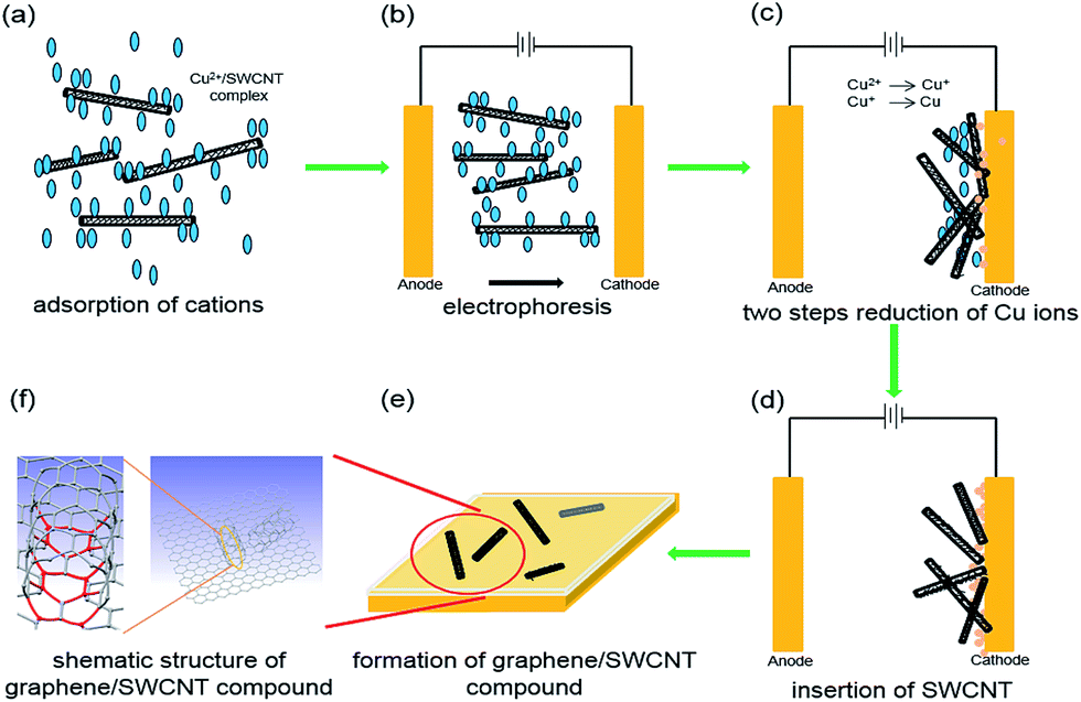 | ||
| Fig. 1 Schematic of fabrication processes for graphene/SWCNT hybrid TCF. | ||
The surface condition is an important factor to elucidate the quality of graphene, including the pre-treatment, fabrication and transfer processes. Fig. 2 shows the surface morphology of three types of TCFs. The SWCNT with a diameter of approximately 3 nm is clearly observed in Fig. 2a. It is easy to understand that the Cu on the anode has a smoother surface and less impurities than that on cathode, and the surface morphology of the Cu substrate is directly proportional to the graphene surface condition. However, the root-mean-square (RMS) of hybrid TCF is only approximately 1.26 nm, which is lower than graphene(c) (1.58 nm) and graphene(a) (2.02 nm). The good surface morphology of hybrid films likely indicates that the SWCNT acted as a “filler” and flattened the rugged Cu surface, thereby increasing the flat level of the catalyst in the CVD process. The SWCNT also played the role of a “soft” buffer that decreased the mismatch in surface morphology between the soft Cu substrate and the rigid SiO2/Si substrate in the transfer process. Thus, a low surface roughness and a small value of RMS on the hybrid films were obtained.20 In order to evaluate the thickness of hybrid film, an artificial scratch was made and the thickness was found to be about 0.8 nm as shown in Fig. 3a and b. The improvement in RMS can be more useful and applicable for its utilization in organic optoelectronic devices because they commonly require good surface morphology.
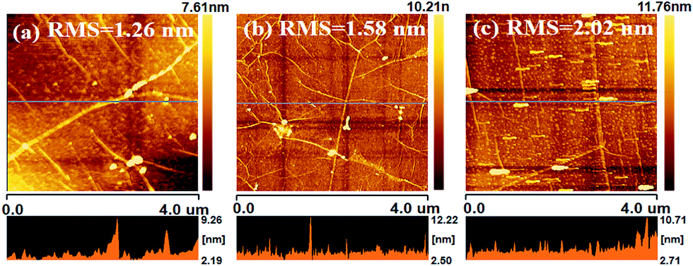 | ||
| Fig. 2 Surface roughness of (a) SWCNT/graphene hybrid thin films, (b) graphene(a), (c) graphene(c), transferred on Si/SiO2 substrate. | ||
 | ||
| Fig. 3 (a) AFM image of SWCNT/graphene hybrid thin films with an artificial scratch, (b) profile plot of the height along the line in (a). | ||
To further investigate the surface condition, SEM images of graphene/SWCNT hybrid TCFs on the SiO2/Si substrate were captured, and the results are shown in Fig. 4a. Fig. 4a shows that SWCNT was perfectly wrapped by the graphene layer, and no damage was observed on the SWCNT, which demonstrates that SWCNT remains stable during the electroplating and CVD processes. Furthermore, no impurities and defects such as wrinkles, folds, cracks and ripples were observed on the graphene layer of hybrid TCF, which also indicates that the TCFs possess a good surface morphology.
 | ||
| Fig. 4 (a) SEM and (b) Raman spectra of TCFs on SiO2/Si substrate at laser excitation wavelength of 532 nm. | ||
Raman spectroscopy, which is a typical and effective method to evaluate the structure and defects of carbon-based low-dimensional materials, was used to evaluate the TCF, and the results are shown in Fig. 4b. Fig. 4b displays the average Raman spectra of 5 points in TCF with excitation wavelength of 532 nm on the SiO2/Si substrate. The low D peak at ∼1350 cm−1 of graphene, which corresponds to the degree of crystallinity and defect, indicates that the CVD graphene has high quality. The two prominent peaks at ∼1570 and 2700 cm−1 can correspond to the G and 2D bands, respectively.21 The G band is created by the E2D phonon at the central area of Brillouin zone, and the 2D band represents double-resonant Raman scattering.22 The peak ratio of G/2D is 0.85, and the symmetric 2D band is centered at 2701 cm−1 with a full width at half maximum of 33 cm−1, which demonstrates that the graphene sheet is monolayer dominated.23,24 The intensities of the G and 2D band peaks of SWCNT are distinctly higher than those of the graphene film possibly because of the SWCNT has a significantly stronger scatter signal. For the hybrid TCFs, the peak G/2D ratio of 0.65 is between those of SWCNT (0.35) and graphene (0.85), which indicates the presence of both CNT and graphene. In addition, the peak at ∼2450 corroborates the combination of CNT and graphene, although its interpretation was still subject to debate.25
To further confirm the crystallinity and the layers of graphene, SAED was conducted on the graphene transferred to TEM grid and the results are shown in Fig. 5. The clear diffraction pattern (Fig. 5a) identifies the good crystallinity of graphene. The line profile of the diffraction patterns (Fig. 5b) demonstrates the monolayer nature of the graphene domain.
 | ||
| Fig. 5 (a) SAED pattern of graphene, (b) profile plots of the diffraction peak intensities along the arrows in (a). | ||
Optical transmittance is an important factor for TCFs. Fig. 6a shows the optical transmittance spectra of TCFs transferred to glass substrates. The optical transmittance of graphene(c) was 96.5%, which was slightly lower than that of graphene(a) (97.2%) at the wavelength of 550 nm. The transmittance difference was mainly caused by the surface impurities of Cu at the anode and cathode. In contrast, the transmittance of hybrid TCF was 95.9%, which is slightly lower than the two others as anticipated. However, the transmittance of hybrid TCF remains higher than 94% in the visible light range of 400–800 nm, whose performance is more than acceptable for its application as TCF. The inset graph of Fig. 6a shows the scene through the SWCNT/graphene hybrid film on glass; the red dotted rectangular shows the area of the sample with the size of 2 × 2 cm2. No vision disparity is observed in the graph, which also confirms the uniformity and transparency of the hybrid films.
 | ||
| Fig. 6 (a) Optical transmittance spectra of TCF. The inset graph is the scene through the SWCNT/graphene hybrid film. (b) Sheet resistance versus optical transmittance of TCF, the inset graphs are the water contact angel results of graphene(a) and SWCNT/graphene. | ||
As an alternative of ITO, the electrical conductivity is the foremost issue of TCF in addition to the optical performance and surface condition. The sheet resistance of three types of TCFs that were transferred onto the SiO2/Si substrates was measured by Hall effect measurement system, and the results are shown in Fig. 6b. Fig. 6b shows that the sheet resistance of the hybrid TCF is 394 Ω sq−1 with a transmittance of 95.9% at the wavelength of 550 nm, which is significantly lower than those of graphene(a) and graphene(c). In particular, few numbers of SWCNT from Fig. 6a can distinctly decrease the sheet resistance of the SWCNT/graphene hybrid films, which confirms that few SWCNTs can add conductive channels and repair line defects to decrease the electrical resistance of CVD-grown graphene. The graphene/SWCNT hybrid films were investigated by Yun and Yang, and it has been shown that the decrease in sheet resistance significantly depends on the CNT concentration.11,26 In this study, the concentration of the SWCNT solution is 0.0004 mg mL−1, which is far below the concentration in the literature with the identical range of transmittance and sheet resistance. In other words, the electroplating method of the CNT to the Cu substrate shows better enhancement effect than the commonly used approach to fabricate graphene/CNT hybrid TCF. For the CNTs that are spin-coated or printed on the target substrate, the physical adhesion of CNT to graphene cannot form effective chemical bonding, which hinders the carrier transport between CNT and graphene. In this study, the CNT was partially embedded in Cu, which acted as the catalyst of graphene; during the deposition process, the chemical bond might form between graphene and CNT. Thus, the contact resistance between graphene and CNT significantly decreased; then, the carrier transport was enhanced compared to conventional methods. Because of the extremely low concentration of the SWCNT solution, good balance between sheet resistance and transmittance for the nanoscale thickness TCF was obtained and further demonstrates that the possible formation of the chemical bond between graphene and CNT strengthens the carrier transport and conductivity.
The wetting properties of TCF to function materials directly affect the final application in optical devices. The Contact Angle Instrument was used to evaluate the wetting performance, and the results are shown in the inset graphs of Fig. 6b. The water contact angles (WCAs) of graphene(a) and SWCNT/graphene are 88.9° and 82.3°, respectively, which indicates that SWCNT/graphene is more hydrophilic than graphene(a). The wetting property of graphene-based TCF is a widely concerned issue, and the WCAs vary from ∼40° to ∼90° in the literature.27,28 It has been widely accepted that the WCA is related to the physicochemical composition, surface roughness, surface functional groups and doping level of graphene-based TCF, which eliminates the equipment error.28 Here, we would not strive to distinguish the specific reason of hydrophilic improvement because it is not the main point of this study. Instead, we would like to emphasize that the increase in wetting property of SWCNT/graphene can be helpful in the application of transparent conductive electrodes in optoelectronic devices.
In this study, we only investigated the SWCNT at a certain concentration with the electroplating target of Cu and corroborated the quality enhancement effect of hybrid TCF. In fact, we believe that the proposed approach is applicable to any conductive CNT and graphene catalyst as long as it requires electro-polishing pre-treatment.
4. Conclusions
In this paper, graphene/SWCNT hybrid TCFs were synthesized by growing graphene on Cu foil using CVD, which was pre-electroplated with conductive SWCNT. The fabricated hybrid film using the proposed approach is proven to have better electrical conductance, better surface morphology and negligible loss in transmittance compared with that grown on an electropolished Cu catalyst. Compared with conventional fabrication approaches of graphene/CNT hybrid TCF, much better opt-electrical performance is obtained at the identical concentration of CNT solution. In addition, the increase in wetting property of SWCNT/graphene can be helpful in the application of TCFs in optoelectronic devices. We have proposed and proven that graphene/SWCNT hybrid thin films fabricated by the one-step CVD growth on the Cu foil substrate, which has been pre-electroplated with conductive CNT, is a simple and effective method to obtain high-quality hybrid TCFs.Conflicts of interest
There are no conflicts to declare.Acknowledgements
This work is financially supported by the National Natural Science Foundation of China (51505270) and the Science and Technology Committee of Shanghai (15590500500).References
- K. Kwak, K. Cho and S. Kim, Sci. Rep., 2013, 3, 2787–2793 CrossRef PubMed.
- S. Chen, L. Deng, J. Xie, L. Peng, L. Xie, Q. Fan and W. Huang, Adv. Mater., 2010, 22, 5227–5239 CrossRef CAS PubMed.
- W. Fu, L. Liu, K. Jiang, Q. Li and S. Fan, Carbon, 2010, 48, 1876–1879 CrossRef CAS.
- D. Hecht, L. Hu and G. Grüner, Appl. Phys. Lett., 2006, 89, 425–428 CrossRef.
- Z. Hu, J. Zhang, Z. Hao, Q. Hao, X. Geng and Y. Zhao, Appl. Phys. Lett., 2011, 98, 66–69 Search PubMed.
- K. S. Novoselov, A. K. Geim, S. V. Morozov, D. Jiang, Y. Zhang, S. V. Dubonos, I. V. Grigorieva and A. A. Firsov, Science, 2004, 306, 666–669 CrossRef CAS PubMed.
- K. I. Bolotin, K. J. Sikes, Z. Jiang, M. Klima, G. Fudenberg, J. Hone, P. Kim and H. L. Stormer, Solid State Commun., 2008, 146, 351–355 CrossRef CAS.
- X. Dong, Y. Shi, Y. Zhao, D. Chen, J. Ye, Y. Yao, F. Gao, Z. Ni, T. Yu, Z. Shen, Y. Huang, P. Chen and L. J. Li, Phys. Rev. Lett., 2009, 102, 135501–213554 CrossRef PubMed.
- K. S. Kim, Y. Zhao, H. Jang, S. Y. Lee, J. M. Kim, K. S. Kim, J. H. Ahn, P. Kim, J. Y. Choi and B. H. Hong, Nature, 2009, 457, 706–710 CrossRef CAS PubMed.
- Y. Fu, B. Carlberg, N. Lindahl, N. Lindvall, J. Bielecki, A. Matic, Y. Song, Z. Hu, Z. Lai, L. Ye, J. Sun, Y. Zhang, Y. Zhang and J. Liu, Adv. Mater., 2012, 24, 1576–1581 CrossRef CAS PubMed.
- V. C. Tung, L. M. Chen, M. J. Allen, J. K. Wassei, K. Nelson, R. B. Kaner and Y. Yang, Nano Lett., 2009, 9, 1949–1955 CrossRef CAS PubMed.
- L. Qiu, Q. Wu, Z. Yang, X. Sun, Y. Zhang and H. Peng, Small, 2015, 11, 1150–1155 CrossRef CAS PubMed.
- W. Wang, S. Guo, M. Penchev, I. Ruiz, K. N. Bozhilov, D. Yan, M. Ozkan and C. S. Ozkan, Nano Energy, 2013, 2, 294–303 CrossRef CAS.
- X. Dong, Y. Ma, G. Zhu, Y. Huang, J. Wang, M. B. Chan-Park, L. Wang, W. Huang and P. Chen, J. Mater. Chem., 2012, 22, 17044–17048 RSC.
- L. Wang, W. Feng, L. Yang and J. Zhang, Acta Phys. Sin., 2014, 2014(63), 176801 Search PubMed.
- E. Bezus, H. Brown and L. Tomaszewski, Plating, 1969, 56, 1234–1239 Search PubMed.
- C. Buelens, J. P. Celis and J. R. Roos, J. Appl. Electrochem., 1983, 13, 541–548 CrossRef CAS.
- J. Fransaer, J.-P. Celis and J. Roos, J. Electrochem. Soc., 1992, 139, 413–425 CrossRef CAS.
- N. Guglielmi, J. Electrochem. Soc., 1972, 119, 1009–1012 CrossRef CAS.
- I. N. Kholmanov, C. W. Magnuson, R. Piner, J. Y. Kim, A. E. Aliev, C. Tan, T. Y. Kim, A. A. Zakhidov, G. Sberveglieri, R. H. Baughman and R. S. Ruoff, Adv. Mater., 2015, 27, 3053–3059 CrossRef CAS PubMed.
- X. Dong, D. Fu, W. Fang, Y. Shi, P. Chen and L. J. Li, Small, 2009, 5, 1422–1426 CrossRef CAS PubMed.
- T. H. Seo, A. H. Park, G. H. Lee, M. J. Kim and E.-K. Suh, J. Phys. D: Appl. Phys., 2014, 47, 315102–315108 CrossRef.
- L. Gao, W. Ren, J. Zhao, L. P. Ma, Z. Chen and H. M. Cheng, Appl. Phys. Lett., 2010, 97, 183–186 Search PubMed.
- V. P. Verma, S. Das, I. Lahiri and W. Choi, Appl. Phys. Lett., 2010, 96, 203108–203111 CrossRef.
- A. C. Ferrari and D. M. Basko, Nat. Nanotechnol., 2013, 8, 235–246 CrossRef CAS PubMed.
- A. L. Gorkina, A. P. Tsapenko, E. P. Gilshteyn, T. S. Koltsova, T. V. Larionova, A. Talyzin, A. S. Anisimov, I. V. Anoshkin, E. I. Kauppinen, O. V. Tolochko and A. G. Nasibulin, Carbon, 2016, 100, 501–507 CrossRef CAS.
- R. Raj, S. C. Maroo and E. N. Wang, Nano Lett., 2013, 13, 1509–1515 CrossRef CAS PubMed.
- A. Ashraf, Y. Wu, M. C. Wang, K. Yong, T. Sun, Y. Jing, R. T. Haasch, N. R. Aluru and S. Nam, Nano Lett., 2016, 16, 4708–4712 CrossRef CAS PubMed.
| This journal is © The Royal Society of Chemistry 2017 |