
 Open Access Article
 This Open Access Article is licensed under a
 Creative Commons Attribution 3.0 Unported Licence
Annealing effect on the photoelectrochemical and photocatalytic performance of TiO2 nanorod arrays
Zheng Xie ab,
Shuang Shuanga,
Lingwei Maa,
Fei Zhua,
Xiangxuan Liub and
Zhengjun Zhang*ac
ab,
Shuang Shuanga,
Lingwei Maa,
Fei Zhua,
Xiangxuan Liub and
Zhengjun Zhang*ac
aState Key Laboratory for New Ceramics and Fine Processing, School of Materials Science and Engineering, Tsinghua University, Beijing 100084, China. E-mail: zjzhang@tsinghua.edu.cn
bHigh-Tech Institute of Xi'an, Xi'an 710025, China
cKey Laboratory of Advanced Materials (MOE), School of Materials Science and Engineering, Tsinghua University, Beijing 100084, China
First published on 6th November 2017
Abstract
TiO2 nanorod arrays (NRAs) with 540 nm length and an amorphous porous structure, were fabricated by oblique angle deposition method. The as-prepared amorphous TiO2 NRAs transform gradually into anatase phase after annealing with a temperature higher than 350 °C, whereas the specific surface area decreases due to the better crystallinity. The intensity of hydroxyl groups increases with enhancing annealing temperature, then decreases above 450 °C. The photocatalytic and photo-conversion properties benefit from the high crystallinity of TiO2 NRAs and high density of hydroxyl groups on the surface. It shows that TiO2 NRAs annealed at 450 °C exhibit the highest photoconversion efficiency and maximum degradation rate of MO, which can be ascribed to the excellent crystallization and the optimum density of hydroxyl groups on the surface of TiO2. The TiO2 NRAs with enhanced crystallinity and fine structures are very promising for photocatalyst materials for environmental protection.
1. Introduction
Since the first report of the generation of hydrogen with water splitting using titanium dioxide (TiO2) as a photoanode by Fujishima, and Honda in 1972,1 TiO2 has been extensively studied and been considered as the most promising candidate for solving environmental concerns due to its cheapness, photo-stability, chemical inertness, nontoxicity, and excellent photocatalytic activity.2 In the past decades, the powder system of TiO2 has been employed intensively for water splitting and pollution degradation.3–5 However, the practical applications of powder photocatalysts have been limited due to the separation and recovery of photocatalysts in the aqueous solution, and the high recombination rate of photogenerated electrons and holes in the suspension.6 Therefore, the immobilization of TiO2 in the form of films has been widely investigated for hydrogen production and pollution degradation using solar energy.7–11To enhance the energy conversion efficiency, one of the strategies is to extend its photo response activity to the visible light, which is the main component of the solar spectrum.12 Accordingly, various attempts have been carried out such as doping with impurities,13–15 coupling with dyes,16,17 and sensitizing with narrow band gap semiconductors.18–20 On the other hand, fabrication of one dimensional (1-D) nanostructures, such as nanotubes, nanowires, nanobelts and nanorods, has been proved to be a promising way to enhance the solar energy conversion efficiency of TiO2, considering the fact that some desirable characteristics, e.g., large surface areas, longer charge carrier diffusion lengths and low reflectivity, can be obtained readily.21 Additionally, 1-D nanostructures can be grown by the oblique angle deposition (OAD),22 which is a simple way to produce large area, uniform and aligned nanorod arrays (NRAs) with controlled porosity.
Among the three crystalline polymorphs of TiO2, anatase and rutile have been widely used in photocatalytic applications.23 The photoactivity of the two crystalline phase is reported inconsistently, which can be ascribed to the difference in the crystal size, specific surface are, and the synthesis method.24 These studies on the effect of crystalline phases have mostly been reported for photocatalysis using nanoparticles and nanotubes.25,26 It has been found that the as grown TiO2 films or columns by physical vapor deposition method under room temperature were typically amorphous,27,28 and annealing at a temperature ranging from 300 to 700 °C in air caused the formation of single anatase crystalline phase,29 and also annealing at 400 and 500 °C under O2 flow varied the porosity and oxygen defect.30 However, the photoelectrochemical and photocatalytic properties were not been discussed.
As we know, heat treatment of TiO2 has a great effect on its grain size, surface morphology, crystalline phase composition, and photoelectrochemical and photocatalytic properties.6 Therefore, it is necessary to further study the effect of annealing temperature on TiO2 NRAs. On one hand, the relationship between annealing temperature and morphology, structure et al. should be demonstrated in order to indicate the revolution of TiO2 NRAs by annealing. On the other hand, it is urgent need to determining optimum parameters to obtain excellent photocatalytic and photo-conversion. To the best of our knowledge, there is few report focus on the effect of annealing temperature for the photoelectrochemical and photocatalytic properties in TiO2 NRAs prepared by oblique angle deposition.
For this purpose, TiO2 NRAs annealed at different temperatures has been studied in this work. The effects of annealing temperature on the crystallization, morphology structures, photoelectrochemical properties, and photocatalytic activity are discussed in order to obtain TiO2 NRAs with higher photocatalytic activity and then to enhance the solar conversion efficiency.
2. Experimental details
2.1 Preparation and heat treatment of TiO2 NRAs
The TiO2 NRAs were deposited on quartz and F-doped SnO2 (FTO) substrates using oblique angle deposition technique (OAD) described elsewhere,18,31 where, the OAD system was built by the electron beam evaporation (DZS-500, SKY Technology Development Co., Ltd. CAS). The substrates were ultrasonically cleaned sequentially in acetone and alcohol, respectively, and then rinsed in deionized water for 5 minutes. Prior to deposition the system was pumped down to a vacuum level of 2 × 10⁻⁵ Pa, and then TiO2 NRAs were deposited at a deposition rate of 0.5 nm s−1, of which the thickness was monitored by a quartz crystal microbalance. In order to produce aligned TiO2 NRAs, the incident beam of TiO2 flux was set at ca. 85° from the normal of the substrate, and the substrate temperature was controlled at ca. −20 °C using liquid nitrogen to maintain the temperature. The substrate remained stationary during deposition. The TiO2 NRAs were annealed in a tube furnace under atmosphere at different temperature (i.e., 300 °C, 350 °C, 450 °C, 550 °C, and 650 °C) for 2 hours, the temperature was carried out at a ramping rate of 5 °C min−1. Note that no annealing temperature higher than 650 °C was used in the experiment, since the glass transition temperature of the glass substrate is approximately 650 °C. For the sake of convenience, we mark the TiO2 NRAs annealed for 300 °C, 350 °C, 450 °C, 550 °C, and 650 °C as 300-TiO2 NRAs, 350-TiO2 NRAs, 450-TiO2 NRAs, 550-TiO2 NRAs and 650-TiO2 NRAs, respectively.2.2 Characterizations
The crystal structure of the TiO2 NRAs was characterized by X-ray diffraction (XRD Rigaku 2500) using Cu Kα radiation (λ = 0.15406 nm). The morphology was characterized by using a field emission scanning electron microscopy (SEM JEOL-7001F). The microstructures of prepared samples were also characterized with a transmission electron microscope (TEM JEOL-2010F). The refractive index (ne) of the TiO2 NRAs films deposited at various oblique angels was measured by spectroscopic ellipsometry (J.A. Woollam, Co., Inc., Lincoln, NE, USA). Transmittance spectra were recorded using a UV-vis spectrophotometer (PerkinElmer Lambda 35). The XPS experiments were performed on the samples with PHI 5300 (Perkin Elmer). The binding energy of the XPS spectra was calibrated with reference to the C 1s peak at 284.6 eV.Photoelectrochemical measurements were performed in a 250 mL quartz cell using a three electrode configuration, which are composed of the prepared samples as a working electrode, a Pt foil as a counter electrode, a KCl-saturated Ag/AgCl as a reference electrode, and 1 M KOH as an electrolyte. The photocurrent intensity versus potential (I–V curve) measurements were performed by an electrochemistry workstation (CHI 660, Chenhua Instrument). The working electrode was tested at the illumination intensity of 250 mW cm−2 using a 300 W Xe lamp without any light filter (CEL-HXF300, Aulight Co., Ltd). The photocurrent dynamics of the working electrode were recorded according to the response to sudden switching on and off at 0 V bias vs. Ag/AgCl electrode. In order to test the photocatalytic activity, methyl orange (MO) was considered as a model contaminant in the purification of dye waste water. The prepared samples (15 mm × 15 mm) were placed in a quartz cell containing 10 mL of MO (5 μM) aqueous solution. The photocatalyst was 5 cm away from the quartz window. The relative concentration of MO in the solution was determined by comparing its UV-vis absorption intensity with that of the initial MO solution at 462 nm.
3. Results and discussion
Fig. 1 displays the XRD patterns of the as-deposited TiO2 NRAs and the TiO2 NRAs annealed in air for different temperature. It can be seen that the as-prepared TiO2 NRAs and 300-TiO2 NRAs exhibit amorphous structure, and after annealing above 350 °C, the amorphous films crystallized to form anatase phase, which peaks are well defined and matched with (JCPDS 21-1272). Pure anatase TiO2 films were obtained with diffractive reflection of (101), (112) and weak (200) peak as shown in Fig. 1. No secondary phases were observed within the detection limit of XRD, which is in agreement with the phase transformation temperature from anatase to rutile in previous literature.32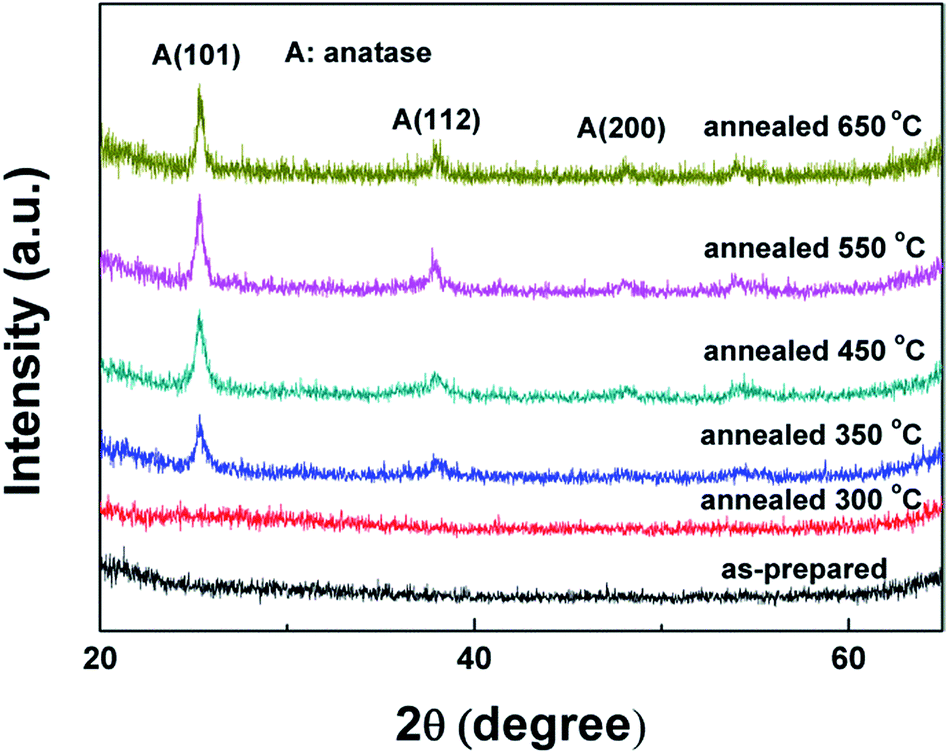 | ||
| Fig. 1 XRD patterns of the as-prepared and annealed TiO2 NRAs at different temperature. | ||
The (101) is the most prevalent face for anatase nanocrystals,33 the (101) peak of annealed TiO2 NRAs becomes stronger and sharper with increasing the annealing temperature from 350 to 650 °C, indicative of better crystallinity. To investigate the influence of crystallite size on the behavior of annealing, the grain size was evaluated using the full width at half maximum (FWHM) of the intense (101) diffraction peak of TiO2 according to the Scherer equation:32
D = Kλ/β![[thin space (1/6-em)]](https://www.rsc.org/images/entities/char_2009.gif) cosθ cosθ |
Fig. 2 presents the SEM images of TiO2 NRAs annealed at various annealing temperature. Top-view image in Fig. 2(a) shows that the as prepared TiO2 NRAs exhibits porous structure consisted of nanorods with diameter of ca. 80–200 nm, and the gap between the nanorods is ca. 25–35 nm. The nanorods are found to be fairly uniform with length of ca. 540 nm shown in the inset of Fig. 2(a), moreover, one can see that the nanorods are tilted with an angle of approximately 22° with respect to the substrate normal due to the high angle of the incident adatom plume to the substrate (α = 85°).35 The porous structure was formed during the deposition process due to the self-shadowing effects and the limited mobility of the deposited atoms.36 The pore size of the TiO2 NRAs becomes lager with increase in gaps between nanorods by annealing at 300 °C which can contributed to the shrink during the annealing process. Further increasing annealing temperature, the morphology of TiO2 NRAs does not change much as shown in Fig. 2(b)–(f).
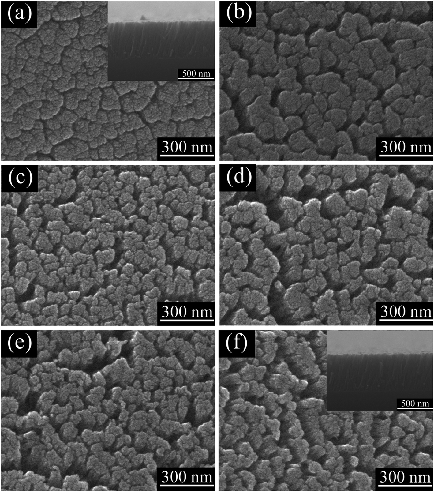 | ||
| Fig. 2 SEM images of samples with various annealing temperature: (a) as prepared, (b) 300 °C, (c) 350 °C, (d) 450 °C, (e) 550 °C and (f) 650 °C, inset images are the cross section view according to (a) and (f), respectively. | ||
In order to further investigate the microstructures of the as-prepared TiO2 NRAs and the annealed one, TEM was performed. Fig. 3(a) shows the low resolution TEM image of the as-prepared TiO2 nanorod. One can see that the nanorod is of length of ca. 540 nm and diameter of ca. 190 nm, which is in agreement with the SEM results. The nanorod exhibits a pine needle structure, leading to a significant enhancement in the overall surface area. This microstructure can facilitate the performance of photoelectrochemistry due to the 1-D structure with high specific surface area.37 Fig. 3(b) displays the high-resolution TEM (HRTEM) image of the as-prepared TiO2 NRAs. There is no lattice fringe in the area as one can see, and the selection area electron diffraction (SAED) as shown in the set of Fig. 3(b) consists of a diffuse halo, indicating that the as-prepared TiO2 NRAs is amorphous.30 The HRTEM images of the sample annealed at 450 and 550 °C are presented in Fig. 3(c) and (d), respectively. According to the images, TiO2 crystalline grains can be seen clearly with interplanar lattice spacing of 0.352 nm, corresponding well with that of (101) plane of anatase. Furthermore, the inset images in Fig. 3(c) and (d) show the SAED of two samples, respectively. The SAED patterns display diffraction rings composed of some separate diffraction spots, exhibiting a polycrystalline feature, which is in agreement with the XRD results.
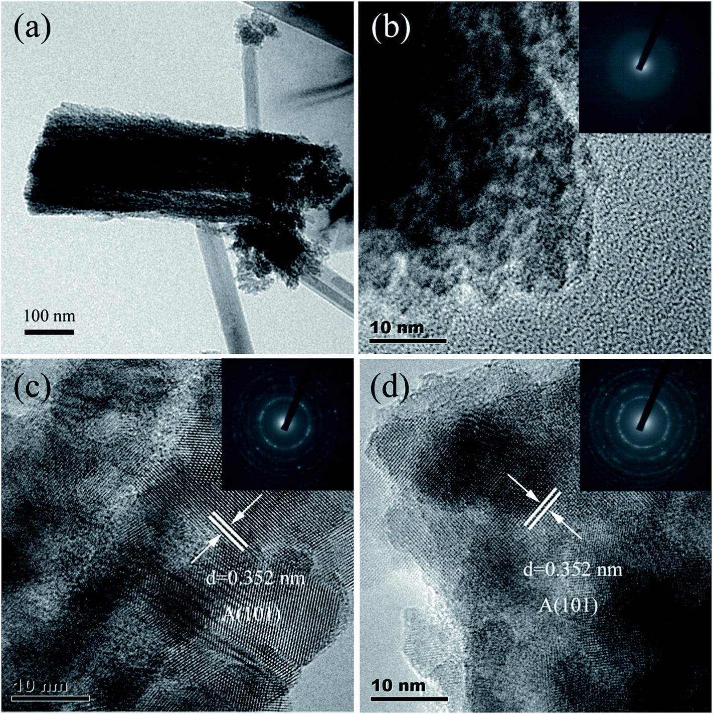 | ||
| Fig. 3 (a) LRTEM and (b) HRTEM images of as prepared TiO2 NRAs, (c) and (d) are HTEM images of TiO2 NRAs annealed at 450 and 550 °C, respectively. Inset images are the SAED patterns according to (b), (c) and (d), respectively. | ||
The refractive index (ne) of the as-prepared and annealed TiO2 NRAs films was measured by spectroscopic ellipsometry at wavelengths from 500 nm to 900 nm. For a clear demonstration, we plot the variation of ne at 600 nm as a function of the deposition angle, which is illustrated in Fig. 4. As the annealing temperature increases from room temperature to 650 °C, ne increases from 1.493 to 1.673, which is the result of the reconstruction of nanostructure as was discussed above. For two non-absorbing components with volume fractions fi and refractive indices ni, the Bruggemann effective medium approximation gives:38
| f1[(n12 − ne2)/(n12 + 2ne2)]+ f2[(n22 − ne2)/(n22 + 2ne2)] = 0. |
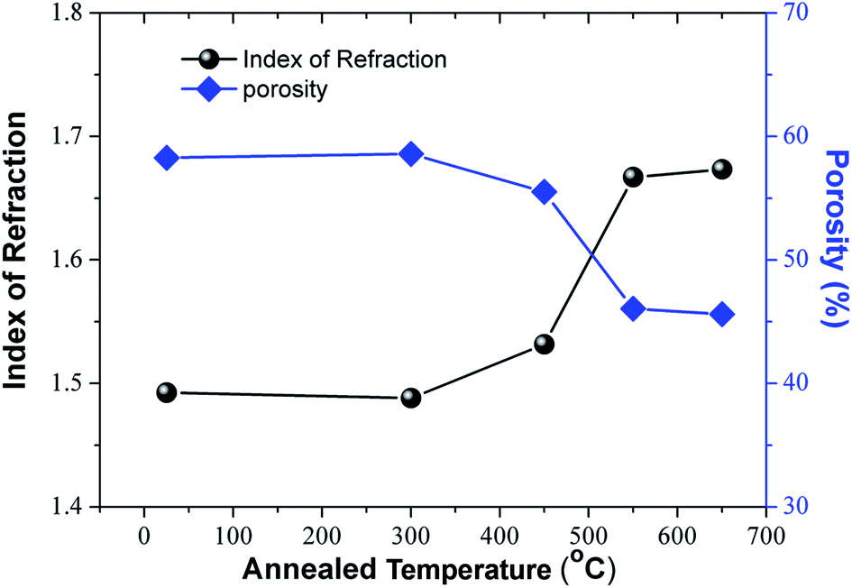 | ||
| Fig. 4 The refractive index at 600 nm and the calculated porosity of the films, as function of the annealing temperature. | ||
Fig. 5(a) shows the UV-visible light transmittance spectra of the TiO2 NRAs annealed for different temperature. The spectra are characterized by a good regularity of the interference fringes and a systematic increment in wavelength in which the film practically ceases to be transparent in the visible range. This behavior has been previously observed in previous report.40 With increase in annealing temperature, the transmittance decreases gradually at the wavelength of 250 nm to 550 nm, in the other hand, the absorption edge exhibits red shifts. The optical gap (Eg) of the semiconductor with large band gap can be determined from the absorption coefficient α. If scattering effect is neglected, the absorption coefficient can be expressed by (αEg)n = A(Eg − hν), where n = 1/2 for an indirect transmission.41 The Tauc42 plot of (αE)1/2 vs. photon energy (E = hν) is shown in Fig. 5(b). Usually, the band gap can be obtained by extrapolating the linear region to (αE)1/2 = 0. The band gap of the as-deposited TiO2 NRAs (amorphous) is ca. 3.45 eV and it decreases to 3.34 eV after annealing at 650 °C. The higher values of band gap observed in our experiment can be associated to the nanocrystalline nature of the TiO2 NRAs which similar to previous report.43 The decrease in the optical band gap of TiO2 NRAs with increase in annealing temperature might be the result of the change in film density and augmentation of size of scattering center.44 During the annealing process, the nanocrystalline grains gradually grow from amorphous, and then the crystalline grains grow larger with increasing annealing temperature and duration.30 In addition, the oxygen vacancies occur on the surface of TiO2 NRAs.30 It is reported that the visible absorption is positively related to oxygen vacancy in TiO2.25,45 With increasing annealing temperature and duration, the number of oxygen defects further decreases along with the crystallization,26 while the size of nanocrystals grows bigger. The former process will increase the band gap, while the latter process will decrease the band gap. The two processes compete with each other, and the latter is the dominant progress in this case, resulting in a slight decrease in the band gap with increasing annealing temperature.30
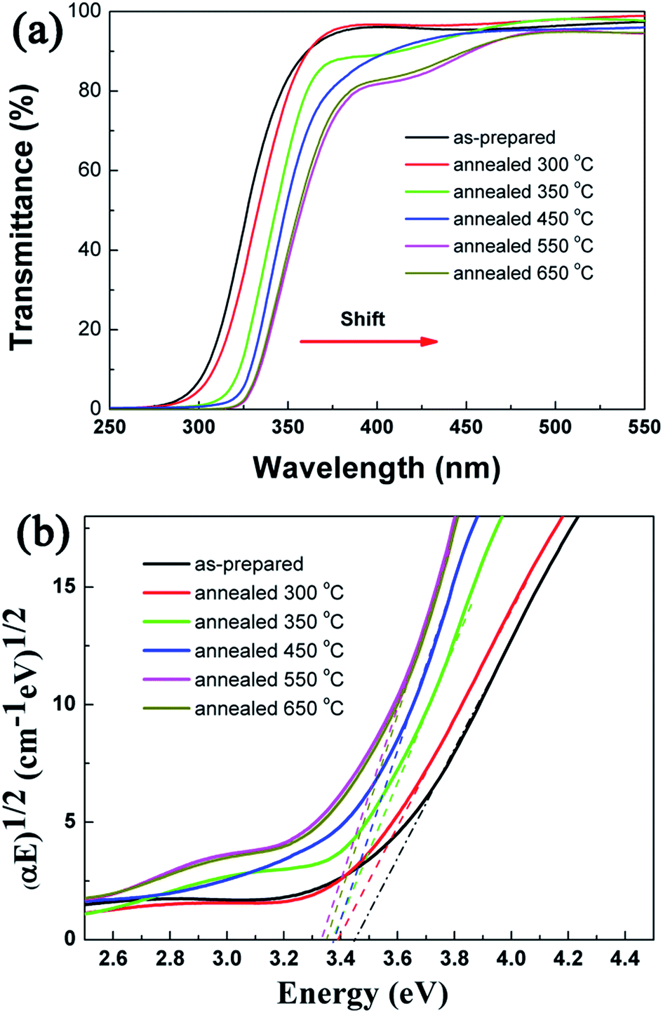 | ||
| Fig. 5 (a) UV-visible light transmittance spectra and (b) the tauc plots of the TiO2 NRAs. | ||
In order to identify the chemical state of TiO2 NRAs, XPS was carried out. As shown in Fig. 6(a), it was found that the two characteristic peaks of Ti 2p1/2 was at ∼465 eV and Ti 2p3/2 was at ∼459 eV in the as-prepared TiO2 NRAs, but there was obvious shift to low binding energy in the two peak positions binding energy peaks of the annealed TiO2 NRAs. This strongly suggested that Ti4+ had trends into transform to lower valance,46 it might suggest migration of electrons bound to oxygen and titanium ions toward oxygen vacancies.25,47,48 The surface oxygen vacancies can trap the photogenerated electrons thus reducing the electron–hole recombination.49,50 Fig. 6(b) shows the O 1s XPS spectra core level of the as-prepared TiO2 NRAs and the ones annealed at 350 °C, 450 °C, 550 °C, 450 °C, and 650 °C, respectively. For the as-prepared TiO2 NRAs, there is a peak at ∼530.1 eV, which is characteristic of intrinsic oxygen corresponding to TiO2, and the other peak at ∼531.6 eV can be ascribed to surface hydroxyl groups in TiO2.51–53 The signals of hydroxyl groups observed should be due to hydroxyl groups, strongly bound to surface defects on TiO2 NRAs annealed at different temperatures, since the physically absorbed hydroxyl groups on TiO2 NRAs can be easily removed under ultrahigh vacuum condition of the XPS system.54 That is, the hydroxyl groups in XPS are associated with surface defects and the visible hydroxyl groups should indicate the existence of surface oxygen defects on TiO2 samples.54–56 Chemisorbed surface hydroxyl groups can enhance photocatalysis by trapping photoinduced holes resulting in an increase in the formation of highly oxidizing OH radicals.57,58 It is reported that the number of surface hydroxyl groups per surface area of anatase TiO2 increases with increasing annealing temperatures.59 In the present case, a similar trend can be concluded for TiO2 NRAs based on XPS results. The rate of O in hydroxyl groups to intrinsic O (O531.6/O530.4) on TiO2 surface increases from 43.17% to 74.1%, with increase in annealing temperature, and obtains the maximum at 450 °C. However, further increasing annealing temperature to 550 and 650 °C, it decreases to 50.3% and 45.7%, respectively. This phenomenon can be ascribed to the grain boundary reduction on surface with the formation of large nanocrystallites by further enhancing the annealing temperature, which results in decrease in surface area. Thus, it is reasonable to expect that a suitable increased number of defects on surface of TiO2 NRAs would result in improved charge transportation and enhancement of photocurrent density.50
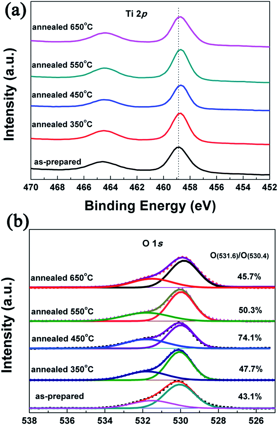 | ||
| Fig. 6 XPS of the Ti 2p (a) and O 1s (b) of TiO2 NRAs annealed at different temperatures. | ||
Photocurrent intensity has been regarded as one of the most efficient method to evaluate the photo-catalytic activity of photocatalyst, and it has been recognized that a high photocurrent intensity suggests a high efficiency for electrons and holes generation and separation, and thus a high photo-catalytic activity.60 I–V curves of TiO2 NRAs annealed at different temperature are shown in Fig. 7(a). Upon illumination, the current gradually increases with increasing applied potential from −0.86 to 0 V, indicating photogenerated electron–hole separation induced by the electric field. At higher potentials (E > −0.2 V), a saturation of the photoresponse is observed for all the samples which is ascribed to the field distribution on the nanorods.61 Theoretically, the open circuit potential corresponds to the difference between the apparent Fermi level of the TiO2 NRAs. For the annealed samples, there is a negative shift in the open circuit potential with increase in annealing temperature from 350 to 650 °C, which suggests a better charge separation and electron accumulation in TiO2 NRAs62 due to the better crystallization after annealing.
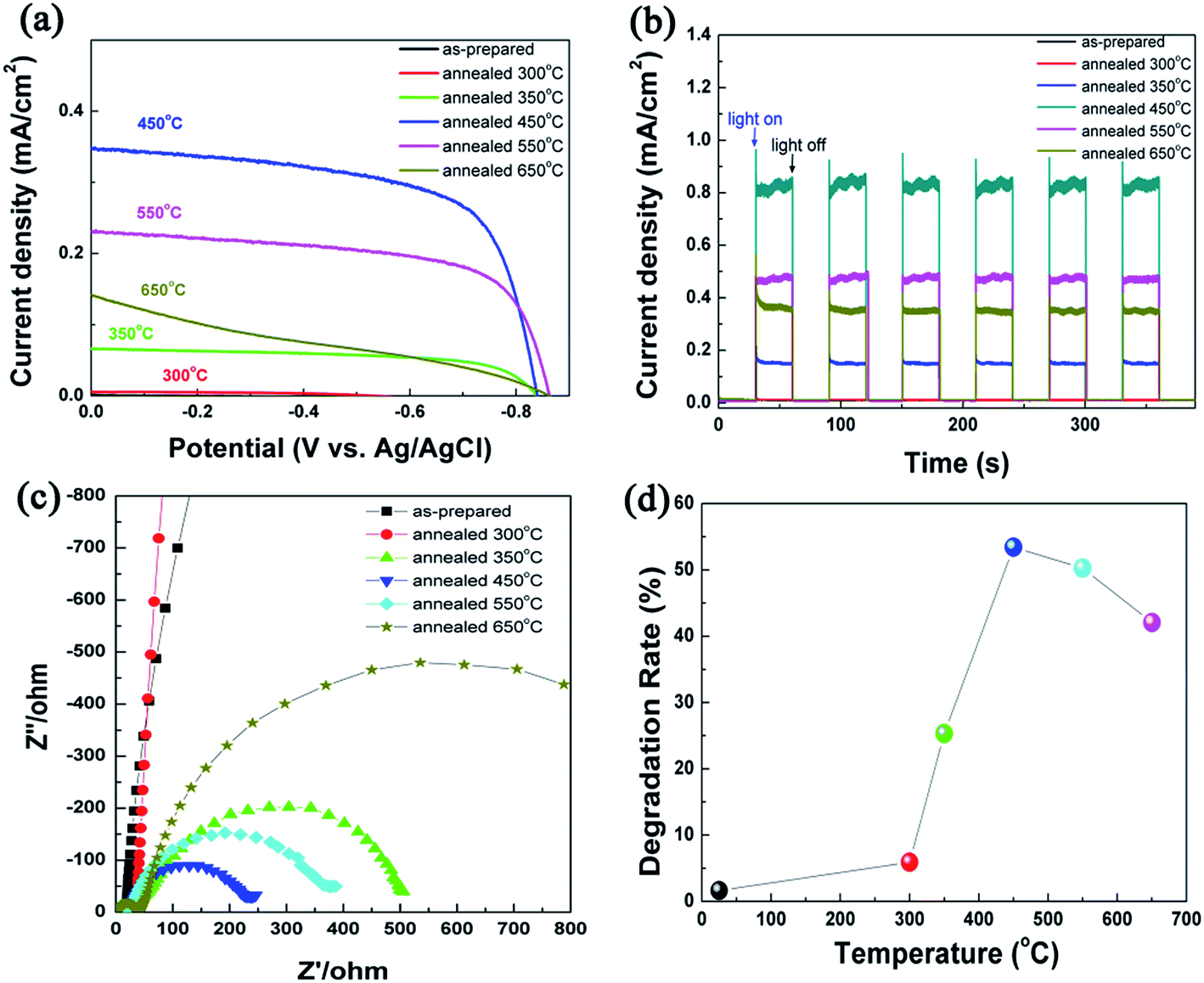 | ||
| Fig. 7 I–V plots (a), I–T plots (b) and EIS responses (c) of TiO2 NRAs, (d) the degradation rate of MO using TiO2 NRAs as photocatalyst. | ||
To further test the photoelectrochemical properties of the TiO2 NRAs annealed for different temperature under irradiation, photocurrent densities were measured in the light on–off process with a pulse of 30 s by the potentiostatic technique.63 The plots of current density vs. potential are shown in Fig. 7(b). The photocurrent intensity of as-prepared TiO2 NRAs and the one annealed at 300 °C can be neglected due to their amorphous structure. For all TiO2 NRAs annealed above 350 °C, the photocurrent value goes down to zero as soon as the light is turned off, and the photocurrent intensity comes back to the original value as soon as the light is turned on again. This result indicates that the charge transportation process from TiO2 NRAs to FTO substrate is very rapid.6
Among annealed TiO2 NRAs, the photocurrent intensity increase with increasing temperature due to the formation of anatase phase and the enhancement of crystallization. TiO2 NRAs annealed at 450 °C exhibit a maximum photocurrent density of ca. 0.36 ± 0.01 mA cm−2. Beyond this temperature, a decrease of photocurrent intensity is observed. When TiO2 illuminated by the photons with energy higher than 3.2 eV, photogenerated electrons and holes form in the conduction band and valance band, respectively. According to literatures,64,65 electrons will transfer in bulk traps and surface states. Electrons transfer of bulk traps only occur in between the bulk traps and the conduction band of TiO2 (ref. 65) whereas the surface states can transfer electrons to the acceptor species in solution in an addition to the electron exchanges with conduction band of TiO2.6 In the present condition, the bulk traps can be regarded as the grain boundary and the amorphous domains between the crystallites within the TiO2 NRAs, whereas the surface states are mainly from the surface oxygen defects on TiO2 NRAs.
Annealing can lead to decrease in the grain boundary and amorphous domains which act as the recombination center, and results in enhancement in photocurrent density. In the meantime, the surface states appear on the surface of TiO2 NRAs and its density enhances first then decreases with increasing annealing temperature. However, the specific surface area of TiO2 NRAs decreases gradually after annealing in air which has been discussed in Fig. 4, which will cause the drop in photocurrent response. As discussed above all, the crystallization, surface states and specific surface area contribute together to the photocurrent density, and it exhibit the maximum at 450 °C.
EIS provides a powerful method for the study of charge transfer and recombination processes at the semiconductor–electrolyte interfaces.66,67 A typical Nyquist plot obtained at the open-circle potentials for the illuminated as-prepared and annealed TiO2 NRAs is shown in Fig. 7(c). It is reported that smaller size of the semicircle arc diameter indicates a more effective separation of the photogenerated pair or a faster interfacial charge transfer to the electron donor acceptor.6,19 All the annealed TiO2 NRAs have a smaller arc diameter than the as-prepared one, and the arc diameter of the TiO2 NRAs become smaller when the annealing temperature increases to 450 °C. Further increasing temperature will make the arc larger. It indicates that the charge carriers separate and transfer more effectively in 450-TiO2 NRAs than the rest of samples, which is in accordance with the I–V and I–T curves mentioned above.
Fig. 7(d) plots the degradation rate of methyl orange after 1 h irradiation under Xe lamp with the intensity of 250 mW cm−2, using TiO2 NRAs as photocatalyst. It is found that the degradation rate is only 1.6% using the as prepared TiO2 NRAs, which can be attributed to the photobleaching. Enhancement of degradation rate is observed by annealed TiO2 NRAs. For example, the degradation rate is 5.9% for 300-TiO2 NRAs, and it increases to 53.4% immediately, the phenomenon can be ascribed to the transition from amorphous to crystal and the increase of hydroxyl group. Further increasing annealed temperature, the degradation rate decreases, the phenomenon is in agreement with the variation of photocurrent intensity.
4. Conclusions
TiO2 nanorod arrays (NRAs) were fabricated by oblique angle deposition technique using e-beam evaporation system. The as-prepared TiO2 NRAs are amorphous and exhibit porous structures made up of nanorods with length of 540 nm. The amorphous TiO2 NRAs transform gradually into anatase phase after annealing temperature is higher than 350 °C. The growth of the crystalline grains is induced by annealing, resulting in shrinkage of optical gaps after annealing. According to XPS analysis, the oxygen defects is detected, and the intensity of hydroxyl groups increase with enhancing annealing temperature, then it decreases when temperature above 450 °C. The photoelectrochemical and photocatalytic results show that TiO2 NRAs annealed at 450 °C exhibit the highest photoconversion efficiency and maximum degradation rate of MO, which can be ascribed to the excellent crystallization and the optimum density of hydroxyl groups of surface of TiO2. The enhanced crystallinity and fine structures of obliquely deposited TiO2 NRAs are very promising for the applications such as photocatalyst material for environmental protection.Author contributions
Zhengjun Zhang and Zheng Xie conceived and designed the experiments; Shuang Shuang and Lingwei Ma contributed to characterization; Zheng Xie and Fei Zhu performed the experiments; Zheng Xie and Xiangxuan Liu analyzed the data. Zheng Xie write the manuscript. All authors read and approved the final manuscript.Conflicts of interest
There are no conflicts to declare.Acknowledgements
The authors are grateful to the financial support by the National Natural Science Foundation of China (grant No. 51701103, 51531006 and 51572148), Research Project by Chinese Ministry of Science and Technology (grant No. 2016YFE0104000) and China Postdoctoral Science Foundation (grant No. 2016M600084).References
- A. Fujishima and K. Honda, Nature, 1972, 238, 37 CrossRef CAS PubMed.
- R. Yuan, T. Chen, E. Fei, J. Lin, Z. Ding, J. Long, Z. Zhang, X. Fu, P. Liu and L. Wu, ACS Catal., 2011, 1, 200–206 CrossRef CAS.
- S. Goldstein, D. Behar and J. Rabani, J. Phys. Chem. C, 2016, 112, 15134–15139 Search PubMed.
- D. Chen, L. Zou, S. Li and F. Zheng, Sci. Rep., 2016, 6, 20335 CrossRef CAS PubMed.
- A. Yiming Xu and C. H. Langford, Langmuir, 2001, 17, 897–902 CrossRef.
- Y. Sun, K. Yan, G. Wang, W. Guo and T. Ma, J. Phys. Chem. C, 2011, 115, 725–733 Search PubMed.
- K. Zhu, N. R. Neale, A. Miedaner and A. J. Frank, Nano Lett., 2007, 7, 69 CrossRef CAS PubMed.
- Y. Wang, L. Zhang, K. Deng, A. Xinyi Chen and Z. Zou, J. Phys. Chem. C, 2013, 111, 2709–2714 Search PubMed.
- C. Wang, X. Zhang, Y. Zhang, Y. Jia, B. Yuan, J. Yang, P. Sun and Y. Liu, Nanoscale, 2012, 4, 5023 RSC.
- X. Wang, S. Zhang, Y. Xie, H. Wang, H. Yu, Y. Shen, Z. Li, S. Zhang and F. Peng, Int. J. Hydrogen Energy, 2016, 41, 20192–20197 CrossRef CAS.
- S. Zhang, Y. Du, H. Jiang, Y. Liu and R. Chen, Ceram. Int., 2017, 43, 7261–7270 CrossRef CAS.
- A. Kudo and Y. Miseki, Catal. Surv. Asia, 2003, 38, 253 Search PubMed.
- C. Burda, Y. Lou, X. Chen, A. C. S. Samia, J. Stout and J. L. Gole, Nano Lett., 2003, 3, 1049–1051 CrossRef CAS.
- T. Ohno, T. Mitsui and M. Matsumura, Chem. Lett., 2003, 32, 364–365 CrossRef CAS.
- J. Xie, X. Pan, M. Wang, L. Yao, X. Liang, J. Ma, Y. Fei, P. N. Wang and L. Mi, Nanomaterials, 2016, 6, 113 CrossRef PubMed.
- Y. Park, S. H. Lee, S. O. Kang and W. Choi, Chem. Commun., 2010, 46, 2477–2479 RSC.
- Y. Cho, W. Choi, C. H. Lee, T. Hyeon and H. I. Lee, Environ. Sci. Technol., 2001, 35, 966–970 CrossRef CAS PubMed.
- Z. Xie, X. Liu, W. Wang, X. Wang, C. Liu, Q. Xie, Z. Li and Z. Zhang, Nano Energy, 2015, 11, 400–408 CrossRef CAS.
- X. Gao, X. Liu, Z. Zhu, X. Wang and Z. Xie, Sci. Rep., 2016, 6, 30543 CrossRef CAS PubMed.
- M. Chang, H. Hu, Y. Zhang, D. Chen, L. Wu and X. Li, Nanomaterials, 2017, 7, 104 CrossRef PubMed.
- H. Zhou, Y. Qu, T. Zeid and X. Duan, Energy Environ. Sci., 2012, 5, 6732–6743 CAS.
- Y. He, Z. Zhang and Y. Zhao, J. Vac. Sci. Technol., B: Microelectron. Nanometer Struct.-Process., Meas., Phenom., 2008, 26, 1350–1358 CrossRef CAS.
- V. K. Mahajan, M. Misra, K. S. Raja and S. K. Mohapatra, J. Phys. D: Appl. Phys., 2008, 41, 125307 CrossRef.
- O. Carp, C. L. Huisman and A. Reller, Prog. Solid State Chem., 2004, 32, 33–177 CrossRef CAS.
- Q. Kang, J. Cao, Y. Zhang, L. Liu, H. Xu and J. Ye, J. Mater. Chem. A, 2013, 1, 5766–5774 CAS.
- D. Zhao, T. Peng, L. Lu, P. Cai, P. Jiang and Z. Bian, J. Phys. Chem. C, 2008, 112, 8486–8494 CAS.
- Z. Li, Y. Zhu, Q. Zhou, J. Ni and Z. Zhang, Appl. Surf. Sci., 2012, 258, 2766–2770 CrossRef CAS.
- M. J. Riley, B. Williams, G. Y. Condon and J. Borja, J. Appl. Phys., 2012, 111, 8269–8285 Search PubMed.
- N. Martin, C. Rousselot, D. Rondot, F. Palmino and R. Mercier, Thin Solid Films, 1997, 300, 113–121 CrossRef CAS.
- Y. P. He, Z. Y. Zhang and Y. P. Zhao, J. Vac. Sci. Technol., B: Microelectron. Nanometer Struct.-Process., Meas., Phenom., 2008, 26, 1350–1358 CrossRef CAS.
- X. Zhang, Q. Zhou, J. Ni, Z. Li and Z. Zhang, Phys. E, 2011, 44, 460–463 CrossRef CAS.
- N. R. Mathews, E. R. Morales, M. A. Cortés-Jacome and J. A. T. Antonio, Sol. Energy, 2009, 83, 1499–1508 CrossRef CAS.
- A. Fujishima, X. Zhang and D. A. Tryk, Surf. Sci. Rep., 2008, 63, 515–582 CrossRef CAS.
- T. Peng, D. Zhao, K. Dai, W. Shi and K. Hirao, J. Phys. Chem. B, 2005, 109, 4947–4952 CrossRef CAS PubMed.
- A. Wolcott, W. A. Smith, T. R. Kuykendall, Y. Zhao and J. Z. Zhang, Small, 2009, 5, 104–111 CrossRef CAS PubMed.
- M. Suzuki, J. Nanophotonics, 2013, 7, 073598 CrossRef.
- Z. Xie, Y. Zhang, X. Liu, W. Wang, P. Zhan, Z. Li and Z. Zhang, J. Nanomater., 2013, 2013, 9 Search PubMed.
- P. K. Ho, D. S. Thomas, R. H. Friend and N. Tessler, science, 1999, 285, 233 CrossRef CAS PubMed.
- M. Jerman and D. Mergel, Thin Solid Films, 2007, 515, 6904–6908 CrossRef CAS.
- A. L. J. Pereira, L. Gracia, A. Beltran, P. N. Lisboa-Filho, J. H. D. da Silva and J. Andres, J. Phys. Chem. C, 2012, 116, 8753–8762 CAS.
- N. Miyata and S. Akiyoshi, J. Appl. Phys., 1985, 58, 1651–1655 CrossRef CAS.
- J. Tauc, J.Optical Properties of Solids, North-Holland Pub, Amsterdam, 1972 Search PubMed.
- N. Mathews, E. R. Morales, M. Cortés-Jacome and J. Toledo Antonio, Sol. Energy, 2009, 83, 1499–1508 CrossRef CAS.
- N. K. Allam and M. A. El-Sayed, J. Phys. Chem. C, 2010, 114, 12024–12029 CAS.
- X. Pan, M. Q. Yang, X. Fu, N. Zhang and Y. J. Xu, Nanoscale, 2013, 5, 3601 RSC.
- F. Liu, L. Lu, P. Xiao, H. He, L. Qiao and Y. Zhang, Bull. Korean Chem. Soc., 2012, 33, 2255–2259 CrossRef CAS.
- M. Senna, V. Šepelák, J. Shi, B. Bauer, A. Feldhoff, V. Laporte and K. D. Becker, J. Solid State Chem., 2012, 187, 51–57 CrossRef CAS.
- A. C. Papageorgiou, N. S. Beglitis, C. L. Pang, G. Teobaldi, G. Cabailh, Q. Chen, A. J. Fisher, W. A. Hofer and G. Thornton, Proc. Natl. Acad. Sci. U. S. A., 2010, 107, 2391–2396 CrossRef PubMed.
- V. Ischenko, S. Polarz, D. Grote, V. Stavarache, K. Fink and M. Driess, Adv. Funct. Mater., 2010, 15, 1945–1954 CrossRef.
- R. Lv, T. Wang, F. Su, P. Zhang, C. Li and J. Gong, Nano Energy, 2014, 7, 143–150 CrossRef CAS.
- M. M. Khan, S. A. Ansari, D. Pradhan, M. O. Ansari, D. H. Han, J. Lee and M. H. Cho, J. Mater. Chem. A, 2013, 2, 637–644 Search PubMed.
- Z. Zhang, X. Wang, J. Long, Q. Gu, Z. Ding and X. Fu, J. Catal., 2010, 276, 201–214 CrossRef CAS.
- H. Zhuang, Q. Gu, J. Long, H. Lin, H. Lin and X. Wang, RSC Adv., 2014, 4, 34315–34324 RSC.
- J. Yan, G. Wu, N. Guan, L. Li, Z. Li and X. Cao, Phys. Chem. Chem. Phys., 2013, 15, 10978 RSC.
- A. Iwabuchi, C. K. Choo and K. Tanaka, J. Phys. Chem. B, 2004, 108, 10863–10871 CrossRef CAS.
- R. Wang, N. Sakai, A. Fujishima, A. Toshiya Watanabe and K. Hashimoto, J. Phys. Chem. B, 1999, 103, 2188–2194 CrossRef CAS.
- J. Xu, Y. Chang, Y. Zhang, S. Ma, Q. Yi and C. Xu, Appl. Surf. Sci., 2008, 255, 1996–1999 CrossRef CAS.
- Y. Wu, Q. Zhang, X. Yin and H. Cheng, RSC Adv., 2013, 3, 9670–9676 RSC.
- J. T. Carneiro, T. J. Savenije, J. A. Moulijn and G. Mul, J. Phys. Chem. C, 2010, 114, 327–332 CAS.
- M. Kong, Y. Li, X. Chen, T. Tian, P. Fang, F. Zheng and X. Zhao, J. Am. Chem. Soc., 2011, 133, 16414–16417 CrossRef CAS PubMed.
- X. Cheng, W. Leng, D. Liu, Y. Xu, J. Zhang and C. Cao, J. Phys. Chem. C, 2008, 112, 8725–8734 CAS.
- M. Jakob, H. Levanon and P. V. Kamat, Nano Lett., 2003, 3, 353–358 CrossRef CAS.
- G. Li, L. Wu, F. Li, P. Xu, D. Zhang and H. Li, Nanoscale, 2013, 5, 2118–2125 RSC.
- R. Kern, R. Sastrawan, J. Ferber, R. Stangl and J. Luther, Electrochim. Acta, 2002, 47, 4213–4225 CrossRef CAS.
- J. Bisquert, A. Zaban, M. Greenshtein and I. Moraseró, J. Am. Chem. Soc., 2004, 126, 13550 CrossRef CAS PubMed.
- F. Fabregat-Santiago, G. Garcia-Belmonte, J. Bisquert, A. Zaban and P. Salvador, J. Phys. Chem. B, 2002, 106, 334–339 CrossRef CAS.
- W. Leng, Z. Zhang, J. Zhang and C. Cao, J. Phys. Chem. B, 2005, 109, 15008–15023 CrossRef CAS PubMed.
| This journal is © The Royal Society of Chemistry 2017 |