DOI:
10.1039/C7RA08316E
(Paper)
RSC Adv., 2017,
7, 54911-54919
Charge transport mechanism in copper phthalocyanine thin films with and without traps
Received
27th July 2017
, Accepted 27th November 2017
First published on 1st December 2017
Abstract
We investigate the charge transport mechanism in copper phthalocyanine thin films with and without traps. Previously, charge transport in polycrystalline thin films has been widely described by the multiple trapping and release (MTR) model, without emphasizing the origin of the traps. In this work, polycrystalline organic thin films with and without traps have been grown by engineering different growth conditions. We find that the density of interface states at the grain boundaries can decide the mechanism of charge transport in organic thin films and completely different charge transport mechanisms can be observed in thin films with and without traps.
Introduction
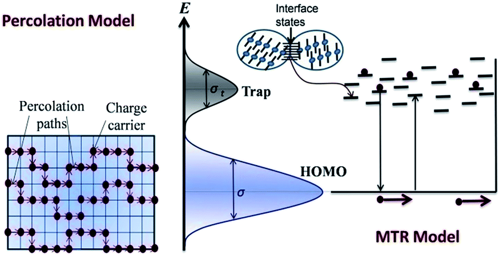
The performance of organic devices based on amorphous1,2 and polycrystalline3,4 thin films depends on the efficiency of charge transport within thin films. In order to improve the performance of these devices, it is necessary to understand the mechanism of charge carrier transport in organic thin films. Copper phthalocyanine (CuPc) has been proved to be interesting and technologically important for applications in organic field effect transistors (OFETs),5 organic light emitting diodes (OLEDs)6 and organic solar cells (OSCs).7 All of these devices are generally based on polycrystalline thin films and cannot be fabricated on single crystals due to poor device integration, cross-talk between devices and low mechanical flexibility.5 Grain boundaries in polycrystalline organic thin films exhibit a large number of barriers and hence limit the charge carrier transport in organic thin film based devices due to trapping and detrapping of charge carriers. It has already been shown5,8 that grain boundaries in organic thin films play an important role in deciding the performance of organic devices and charge transport in these devices can be significantly improved by engineering the growth parameters so that thin films with smaller numbers of grain boundaries can be obtained. However, there appears to be little investigation on how mechanism of charge transport in polycrystalline organic thin films gets affected when (i) density of grain boundaries is varied (ii) shape of the grains is varied and (iii) interface traps at the interface of grain boundaries are varied. Though, several models based on either analytical or simulation have been developed to investigate the charge transport mechanism in organic thin film,9,10 two majorly discussed models to explain the transport mechanism in polycrystalline organic thin films are: multiple trapping and release (MTR) model11–13 and percolation model (PM).14
PM based on variable range hopping within the energetic states in the Gaussian density of states (GDOS) of highest occupied molecular orbital (HOMO) and lowest unoccupied molecular orbital (LUMO) (schematically shown in the left panel in Fig. 1) usually accounts for the carrier transport in amorphous films. Organic polymer thin films which are otherwise amorphous, consist of low density of trap states.15 However, the carrier transport in polycrystalline thin films is usually described by the ubiquitous model, known as MTR.
 |
| | Fig. 1 Schematic representation of charge transport in a p-type organic semiconductor, according to the percolation model based on variable-range-hopping (left panel) and multiple trapping and release model (right panel). | |
According to this model,16,17 charge transport is controlled by traps which are energetically located between HOMO and LUMO, as schematically shown in the right panel of Fig. 1. Most of the charge carriers reside at traps and temporarily get released to HOMO or LUMO, depending upon the position of the trap level and temperature. Surprisingly, the most important aspect of this model i.e. trap is always casually treated without emphasizing where the trap is or what is the origin of the trap in polycrystalline thin films.
Predominantly, there are two sources of traps in organic thin films: chemical impurities and interface states at grain boundaries.18–20 The chemical impurities can be reduced by repeated sublimation, but it is difficult to get rid of traps at grain boundaries in polycrystalline thin films. Although, there are several studies12,21 proposing MTR model to explain charge transport in polycrystalline organic thin films, but it is not clear at all how MTR model can be applied when the density of traps reduced substantially. In view of inapplicability of MTR model, we have explored whether percolation based model could be used in case of polycrystalline thin films.
In this work, we have undertaken detailed investigation on charge transport mechanism in copper phthalocyanine (CuPc) thin films with and without traps by using a combination of two and three terminal devices so that charge transport can be studied along perpendicular and parallel to the film surface. We show that MTR model can explain the charge transport in the polycrystalline organic thin films having intrinsic traps at the grain boundary interfaces. However, it fails to explain the charge transport in polycrystalline thin films having nano-wire like structures with less grain boundaries in which there is either no or negligible quantity of traps. Surprisingly, the PM model explains the charge transport in these films which has more propensity towards crystallinity rather than being amorphous. Charge transport mechanisms in two terminal devices based on thin films with and without traps have also been found completely different.
Experimental details
CuPc, a co-planar organic molecule, has been chosen for this study for two reasons, (i) its exceptional thermal and chemical stability5 and (ii) its ability to grow with different surface morphologies, required to have thin films with and without intrinsic traps. It seems impossible to attain the desired morphology with linear molecule, such as pentacene or any other acenes. High purity (>99.999%), triple sublimed CuPc, procured from Sigma Aldrich Chemical Co. USA has been used for this study to avoid any traps induced due to chemical impurities. For two terminal devices, 200 nm single layer of CuPc was sandwiched between ITO and Au or Al and Au. Thin films were deposited in oil free evaporation system at a base pressure of 5 × 10⁻⁶ mbar. For three terminal organic field effect transistors (OFETs), the heavily doped Si wafers with 300 nm SiO2 layer were used as substrate. 100 nm thick CuPc films were deposited on the substrate with a deposition rate of 0.1 Å s−1 and at different substrate temperatures (TG). Finally, Au was deposited on the organic layer to form the source and drain contacts. The devices had an identical channel width of 3 mm and channel lengths of 20 μm.
The grain boundaries in polycrystalline thin films are difficult to characterize, as the grains are too small to allow for measurements across individual grain boundaries. In case of poly-Si TFTs, several methods based on change in capacitance due to trapping and detrapping of charge carriers have been employed to characterize traps due to grain boundaries.21–23 Unfortunately, none of these methods can be applied in polycrystalline organic thin films for their high resistivity and low carrier mobility. In view of these problems, techniques based on steady state or quasi-static measurements are desirable for the characterizations of defects in organic devices.24 The electrical characterizations of two terminal devices and OFETs were carried out in rough vacuum (10−2 mbar) and using Keithley 485 picoammeter and Keithley 228A and Agilent E3643A voltage sources. In case of organic semiconductors, separation of bulk conduction known as space charge limited conduction (SCLC), which dominates when there is either no or small barrier at metal/organic interface from contact limited conduction known as injection limited current (IJL) which dominates when there exists a barrier at metal/organic interface is extremely important. We have considered two sandwiched devices, based on CuPc (ITO/CuPc/Au and Al/CuPc/Au). CuPc is a hole transport material with HOMO and LUMO at 4.8 eV and 3.0 eV, respectively.25 The work functions of Al, ITO and Au are 4.2 eV, 4.8 eV and 5.2 eV, respectively. There would be either no or very small barrier for holes at Au/CuPc and ITO/CuPc interfaces, but a barrier of 0.6 eV exists at Al/CuPc interfaces.25,26
Organic thin films with and without traps
Organic materials were repeatedly sublimed to reduce impurities related traps as much as possible. But, to reduce structural disorder induced traps, it is required to engineer the growth parameters such as substrate temperature and evaporation rate, to have a certain morphology which results thin films with and without traps.27 Traps due to structural disorder can be reduced substantially by growing organic thin films at low evaporation rate (FG).5 At low FG, incoming molecules have enough time to obtain a favorable orientation resulting ordered growth with minimum structural disorders. Fig. 2 shows the AFM images of CuPc thin films grown at different substrate temperatures (TG) (30 °C to 120 °C) with a fixed evaporation rate of 0.1 Å s−1 on SiO2 surfaces. The grain size and shape vary gradually from isotropic at low TG (30 °C) to anisotropic morphology at higher TG. The CuPc films deposited at substrate temperature of 30 °C show nucleation growth having roughly uniformly distributed grains. Thin films deposited at 60 °C exhibit elongated grains with larger dimensions which convert into rod-like lamellae at 120 °C. This is attributed to the fact that at relatively low substrate temperature, the kinetic energy of the molecules is low and molecules are unable to migrate to meet the other existing islands and get adsorbed at random sites resulting new nucleation centers. Thus nucleation rate dominates the lateral growth resulting into polycrystalline grainy structure with almost equal sized grains (40–60 nm) and a large number of grain boundaries. These grain boundaries act as traps for the charge carriers and hinder the charge transport between source and drain in OFET.5 At relatively high TG, diffusion of molecules on the surface increases leading to the coalescence of already existing grains and clusters.
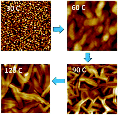 |
| | Fig. 2 AFM topographic (1 μm × 1 μm) images of CuPc thin films, deposited on SiO2 at substrate temperatures (TG) varied from 30 °C to 120 °C with a fixed evaporation rate of 0.1 Å s−1. | |
Hence as TG increases, lateral growth starts dominating the nucleation growth, resulting unidirectional attachment of the molecules at higher TG. This preferential direction of growth is due to π–π interactions along the adjacent molecules and results into greater sticking coefficient along this direction, under growth conditions of higher TG and low FG.
Hence desired morphology of thin films with and without grain boundaries can be obtained by varying the growth parameters (TG and FG) appropriately.
Arrangement of molecules in CuPc thin films
Fig. 3(a) shows the X-ray diffraction (XRD) pattern of CuPc thin film grown at 120 °C. The XRD pattern exhibits a strong peak at 2θ ∼ 6.8° which is due to (100) plane confirming α-phase triclinic structure.28 From XRD, it can be concluded that bc-plane lies parallel to the substrate and is relevant for charge transport in OFET. Fig. 3(b) shows the arrangement of CuPc molecules in OFET geometry. In this plane, CuPc molecules adopt stacking along b-axis. Fig. 3(c) shows the arrangement of CuPc molecules perpendicular to the substrate i.e. along a-axis which is relevant for charge transport along perpendicular to bc-plane i.e. in two terminal sandwiched devices. The XRD pattern of CuPc thin films grown at 30 °C is identical, except the intensity of peak is less than that in thin film grown at 120 °C.
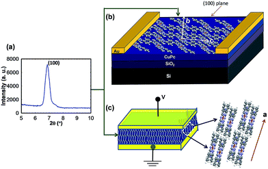 |
| | Fig. 3 (a) XRD of CuPc thin film grown at 120 °C on SiO2 substrate. Schematic representation of arrangement of CuPc molecules (b) in a plane parallel to the substrate and (c) perpendicular to the substrate. These are relevant planes for charge transport in three and two terminal devices, respectively. | |
Transport along a-axis
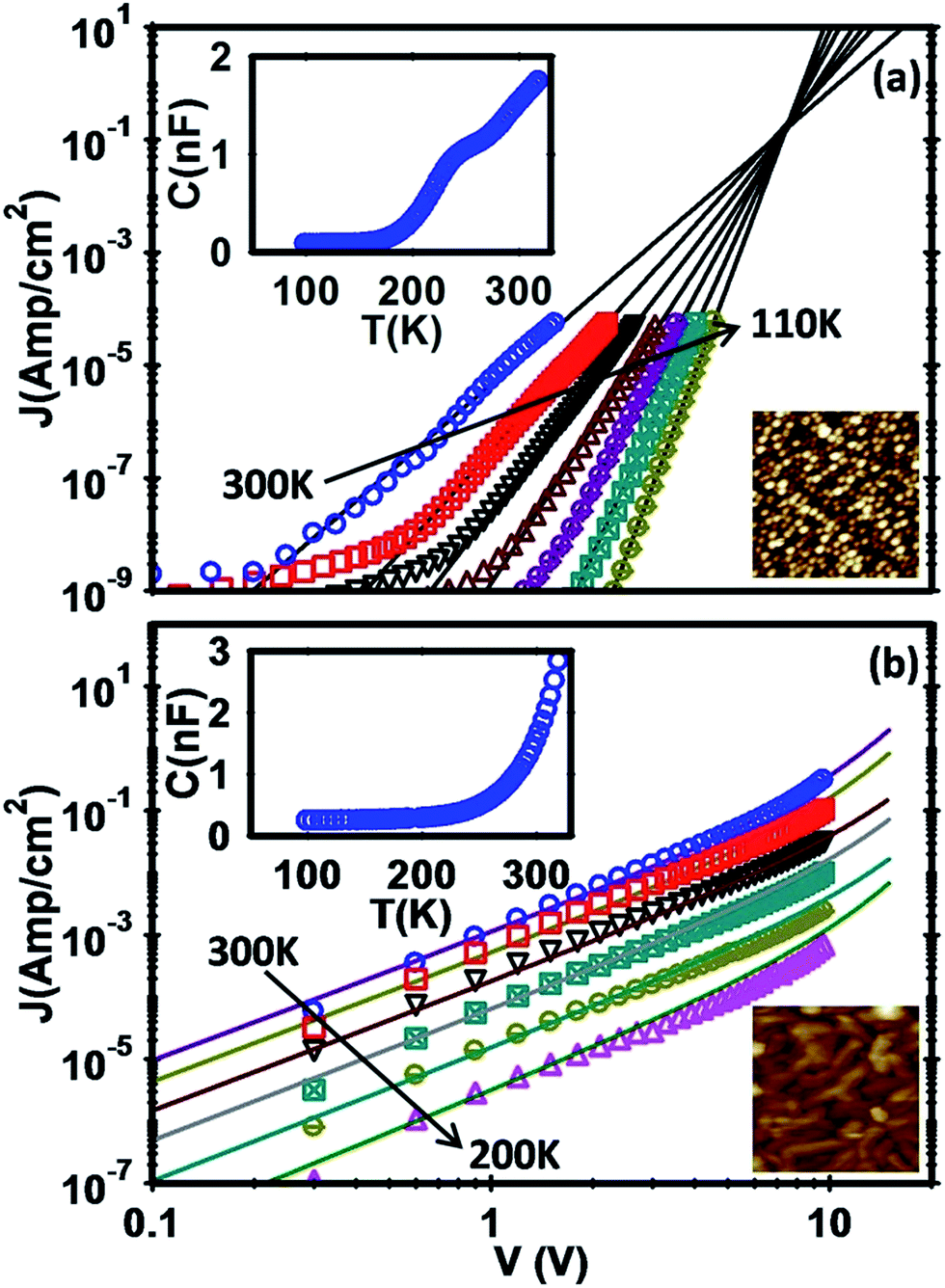
J–V and C–T characteristics of two terminal devices with and without traps
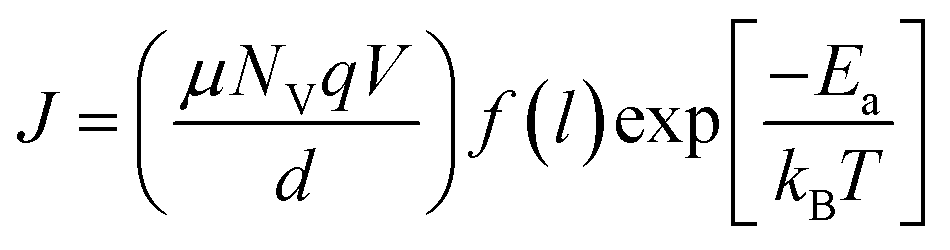
Fig. 4 shows the current–voltage (J–V) characteristics of ITO/CuPc/Au based two terminal devices in which CuPc thin films were grown at TG = 30 °C and 120 °C. In Fig. 4(a), initially, the current increases linearly (ohmic region) due to the thermally generated charge carriers. As the bias increases, current increases more than fourth power of voltage due to trap charge limited conduction (TCLC), following J ∝ Vl+1 (l > 1).29,30 This has been attributed to the exponential or Gaussian distribution of traps30,31 which is further corroborated by a clear step at 230 K in capacitance temperature (C–T) characteristics obtained from thermally stimulated capacitance (TSCAP)32 measurements, shown in the upper inset of Fig. 4(a). This step is observed due to combined effect of two processes; one generation of carriers with temperature and other loss of carriers due to trapping. The midpoint of the step has been used to determine the trap level (Et), given by,32 Et = kBTm![[thin space (1/6-em)]](https://www.rsc.org/images/entities/char_2009.gif) ln(αTm4/β), where Tm is the midpoint of the step, kB is the Boltzmann's constant, α ∼ 1 K−3 s−1 and β is the heating rate which is kept constant at 5 K min−1 during C–T measurement. A step at 230 K corresponds to the trap level at 0.5 ± 0.05 eV which confirms the existence of deep traps in CuPc thin films grown at low TG. In TCLC regime, J–V characteristics of two terminal devices, in the Arrhenius form can be expressed as31,33
ln(αTm4/β), where Tm is the midpoint of the step, kB is the Boltzmann's constant, α ∼ 1 K−3 s−1 and β is the heating rate which is kept constant at 5 K min−1 during C–T measurement. A step at 230 K corresponds to the trap level at 0.5 ± 0.05 eV which confirms the existence of deep traps in CuPc thin films grown at low TG. In TCLC regime, J–V characteristics of two terminal devices, in the Arrhenius form can be expressed as31,33| |
 | (1) |
where  and Ea is the activation energy, given by
| |
 | (2) |
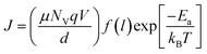
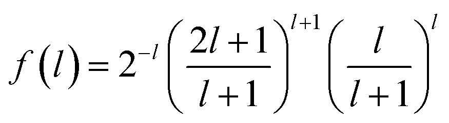
where q is the elementary charge, NV is the effective density of the states (DOS) in the HOMO of CuPc, μ is the mobility of charge carriers, Ntot is the density of trap states, d is the thickness of the thin film and ε is the dielectric constant of organic molecular semiconductor. f(l) ≈ 0.5 when l > 2. Further from Fig. 4(a), it can be seen that the current is temperature independent at a particular voltage Vc, where Ea must be zero. So one gets from eqn (2),| |
 | (3) |
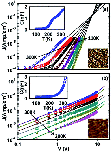 |
| | Fig. 4 Temperature dependent J–V characteristics of ITO/CuPc/Au based sandwiched devices in which CuPc thin films were grown at substrate temperature of (a) 30 °C and (b) 120 °C. Solid lines represent the theoretical fitting with TCLC [eqn (1)] (a) and SCLC with field dependent mobility [eqn (4)] (b), respectively. Upper insets show TSCAP measurements of Al/CuPc/Au based sandwiched devices with heating rate of 5 K min−1 in which CuPc thin films were grown at substrate temperature of (a) 30 °C and (b) 120 °C. Lower insets show the AFM (1 μm × 1 μm) of the CuPc thin films grown on ITO at substrate temperature of (a) 30 °C and (b) 120 °C. | |
By extrapolating, log(J)–log(V) characteristics at various temperatures, Vc and Ntot are found to be ∼8 V and 5.8 × 1016 cm−3, respectively. Ntot is actually the concentration of interface states at grain boundaries, as will be shown below.
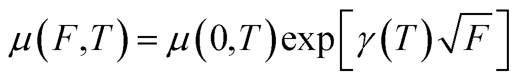
Fig. 4(b) shows the J–V characteristics of ITO/CuPc/Au based two terminal devices in which CuPc thin films were grown at TG = 120 °C. Initially, the current increases linearly in this device, but as the bias increases, injected carrier density exceeds the intrinsic free carrier density and current follows SCLC.34,35 SCLC is observed when there is either no or very low density of traps. In SCLC regime, slope starts from 2 and eventually increases with bias due to the field dependent carrier mobility μ(F,T), given by36
| |
 | (4) |
where
μ(0,
T) is the zero field charge carrier mobility and
γ(
T) is the field activation factor.
J–
V characteristics have been simulated by solving the Poisson's equation, d
F/d
x =
qp(
x)/
ε, describing the relationship between the electric field,
F and the local charge density,
p(
x) and continuity equation,
J(
x) =
qp(
x)
μ[
F(
x),
T]
F(
x) simultaneously.
34 Upper inset of
Fig. 4(b) shows the TSCAP measurements of the corresponding device. We observe that there is no step in
C–
T characteristics. SCLC and absence of step further corroborates the absence of charge carrier traps in CuPc thin films grown at high
TG. Lower insets in
Fig. 4(a) and (b) show the surface morphology of CuPc thin films grown on ITO at
TG = 30 °C and 120 °C, respectively. As discussed earlier, thin films at low
TG show nearly uniform distribution of isotropic grains and hence large number of in-plane interface states at grain boundaries. Charge carriers injected from ITO can be initially trapped by these large number of in-plane interface states in the first monolayer, resulting into TCLC along the perpendicular to the film. However, thin films at high
TG show rod like elongated nanowires providing very few soft grain boundaries, there will be less possibility of charge carriers injected from ITO, getting trapped by the in-plane interfacial states and charge transport occurs by the SCLC. We can conclude that charge transport, perpendicular to the film grown at low and high
TG takes place by two completely different mechanisms.
Characterization of traps from C–f characteristics
Fig. 5 shows the comparison of capacitance–frequency (C–f) characteristics of Al/CuPc/Au based Schottky diodes with traps (empty circles) and without traps (empty squares), under forward and reverse bias. In forward bias, initially, the capacitance decreases with frequency but beyond a certain frequency capacitance becomes independent of frequency. At higher frequency carriers are no longer able to follow the ac signal and contribution due to diffusion capacitance diminishes.37 A step in C–f characteristics of the diodes with deep traps has been observed at ∼1 kHz due to traps whereas this peak is absent in diodes without traps. In case of reverse bias, the capacitance is mainly determined by the depletion capacitance in low frequency region (in both the diodes with and without traps) and remains unresponsive at high frequency regions. Hence, under reverse bias, C–f characteristics of the diodes with and without traps are quite similar. In the forward bias, C–f characteristics over a wide range of frequency have been used to determine the energetic position and density of trap states.36 At low frequency, all the traps are filled whereas at high frequency only those traps below certain demarcation energy (Eω) will be filled and contribute to capacitance. Eω is given by38,39| |
 | (5) |
where ν denotes an attempt-to-escape frequency, which is typically order of 1012 s−1 and ω = 2πf, the angular frequency of the ac signal. So by varying the frequency, we can obtain the density of traps as a function of trap level. Following this approach, the traps distribution can be related to the derivative of the capacitance with respect to frequency and is given by37| |
 | (6) |
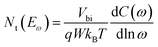
where W is the width of the depletion region and Vbi is the built-in potential due to different work functions of metal electrodes.40 Inset of Fig. 5 shows the energetic distribution of trap states obtained by differentiating the C–f characteristics of Al/CuPc/Au based Schottky diodes with traps, under forward bias (2 V). Gaussian energetic distribution of traps has been observed in devices in which CuPc films were grown at low TG. Width of energetic distribution of traps and position of the trap level with respect to HOMO has been obtained by fitting the experimental data with Gaussian distribution of traps as41| |
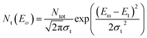 | (7) |
where σt is the width of energetic distribution of traps. Density of trap states as a function of energy along with fitting with eqn (7), results σt of 0.04 eV and the trap level at around 0.50 eV. The value of Et matches well with those obtained independently from C–T characteristics. Hence C–f characteristics also corroborate the existence of deep traps in devices in which thin films were grown at low TG.
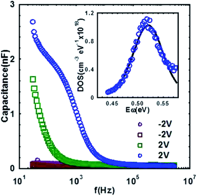 |
| | Fig. 5 C–f characteristics of Al/CuPc/Au based Schottky diodes in which CuPc thin films were grown at substrate temperature of 30 °C (empty circles) and 120 °C (empty squares). Insets show the energetic distribution of trap states obtained from C–f characteristics of the devices grown at 30 °C. Traps are absent in thin films grown at 120 °C. Solid line is fit with Gaussian [eqn (7)]. | |
Charge transport in bc-plane
Charge transport mechanism in OFETs with and without traps
The charge transport in bc-plane in CuPc has been investigated in field effect transistor (FET) geometry. To investigate the impact of the interface states on the charge transport mechanism in some quantitative way, we have estimated the maximum surface density of interfacial traps (Ns) in CuPc thin films grown at low and high TG. Subthreshold swing (SS) is an important OFET parameter that can be used to estimate the density of these traps as,42–44 Ns = [SSlog(e)kBT/q − 1]Ci/q2, Ci being the capacitance of dielectric constant per unit area. SS itself is estimated as,42 SS = [dlog(IDS)/dVG] − 1. SS for the OFETs fabricated at low and high TG have been found to be 9.8 V per decade and 4.89 V per decade, respectively. Then Ns calculated form SS have been found to be 1.04 × 1013 cm−2 eV−1 and 5.18 × 1012 cm−2 eV−1, for the OFETs at low and high TG, respectively. It means that high density of grain boundaries creates additional interfacial traps in the CuPc thin films at low TG.
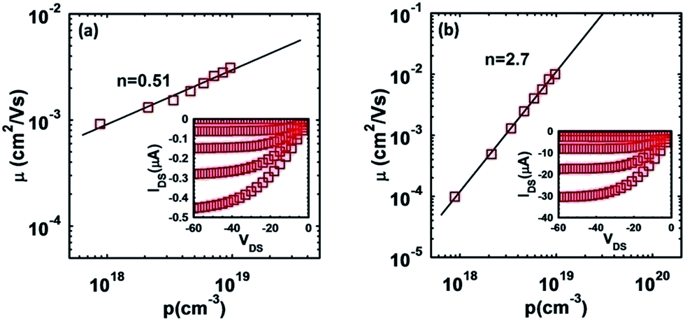
Next, to understand the charge transport mechanism in polycrystalline thin films with different concentration of interfacial traps, μ as a function of carrier concentration (p) for the OFETs based on CuPc thin films with and without traps have been plotted in Fig. 6(a) and (b), respectively. Insets in Fig. 6(a) and (b) show the room temperature output characteristics (IDS–VDS) of the respective OFETs at different VG. IDS in OFETs without traps are almost two orders of magnitude higher than that in OFETs with traps. μ at different p have been calculated from the linear region of the (IDS–VDS) using the relation26
| |
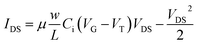 | (8) |
where
w is the channel width,
L is the channel length and
VT is the threshold voltage.
p has been calculated using the relation,
p =
Ci(
VG −
VT)/
qt,
t, being the thickness of the accumulation layer and has been taken 10 nm. The linear relation for the log(
μ)–log(
p) plots suggests the power law dependence of
μ on
p i.e. μ ∝
pn, where
n is the temperature dependent parameter.
 |
| | Fig. 6 Dependence of room temperature charge carrier mobility (μ) on charge carrier concentration (p) in CuPc based OFETs fabricated at substrate temperature of (a) 30 °C and (b) 120 °C. Insets show the room temperature IDS–VDS characteristics of respective OFETs at different VG with a step of 20 V. Solid lines are power law fit μ ∼ pn, where n = TMTR/T − 2 or TPM/T − 1, according to eqn (9) and (10), respectively. | |
Further, we observe the larger modulation in μ with VG for the OFETs without traps compared to those with traps. Generally, the dependence of μ on p in OFETs can be explained as follows. Upon increasing VG, the injected carriers fill the traps at grain boundaries and lower energy states at the edge of the HOMO or LUMO in the organic semiconductors and any additional charges will start to fill higher energy states towards the center, which require low activation energy to hop away to the neighboring sites, resulting higher μ with increasing VG i.e. with increasing p. Hence for OFETs with traps, most of the charge carriers are captured by the interface states at grain boundaries i.e. grain boundaries impose significant barriers and prevent the charge carriers from reaching to transport level. Whereas for OFETs without traps, injected carriers easily fill the lower energy hopping sites existing in the tail of the GDOS and additional carriers occupy higher energy sites, resulting a sharp increase in mobility. In a recent study, similar effect of grain boundaries on the current modulation with gate bias has been observed.45
MTR or PM
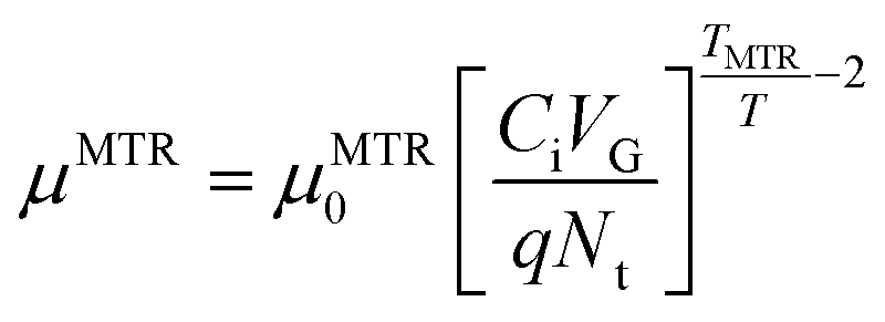
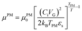
Now, let's apply two well known models: MTR11,12 and PM14 to the OFETs with and without traps. In the MTR model, the localized levels between HOMO and LUMO serve as traps for charge carriers. Depending on the trap depth, T and VG, the carriers temporarily get released by thermally activated process to HOMO. Under the influence of VG, μ gradually increases due to increased carrier concentration excited to the extended states i.e. activation of carriers from a localized state to HOMO. According to this model the charge carrier mobility, μ in OFETs is given by17| |
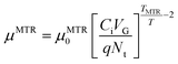 | (9) |
where μMTR0 is weakly temperature dependent prefactor, TMTR is the characteristics temperature which defines σt for the trap states as σt = kBTMTR. From Fig. 6(a) and (b) and using eqn (9), we get TMTR, 753 K and 1410 K for the devices with and without traps, respectively and the corresponding width of the energetic distribution of trap states are found to be 61 meV and 130 meV respectively. The width of energetic distribution of traps (∼60 meV) obtained from MTR model for CuPc thin films grown at low TG matches well with the value obtained from C–f characteristics but the value obtained for thin films grown at high TG is more than the width of HOMO (100 meV).
Moreover, MTR model estimates, the width of energetic distribution of traps to be larger for the OFETs without traps than for the OFETs with traps which is contradicted. Hence charge transport in organic thin films having traps is governed by MTR model but the same model is not applicable for thin films without deep traps. However, same data can be analyzed by PM. According to this model,14 charge carriers move due to thermally activated hopping within the localized states in the energetically distributed density of states (DOS) of HOMO or LUMO. In this model, the charge carrier mobility, μ in OFETs is given by14,46
| |
 | (10) |
where
μPM0 is weakly temperature dependent prefactor and
TPM is the characteristic temperature which represents the width of HOMO and LUMO as
σPM =
kBTPM. From
Fig. 6(a) and (b) and using
eqn (10), we get
TPM, 453 K and 1110 K in the devices with and without traps respectively and the corresponding width of the DOS are found to be 45 and 95 meV, respectively. The calculated width of the DOS for OFETs without traps is around ∼100 meV which is the typical width of the HOMO or LUMO in organic semiconductors.
47 The unusually low value of width of DOS with traps indicates that PM model which is otherwise successful
48 in case of OFETs without traps, is not suitable for OFETs having traps.
Temperature dependence of μ in bc-plane of CuPc thin films with and without traps
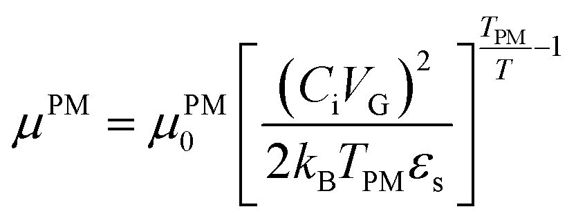
To justify our arguments on the charge transport mechanism in the OFETs with and without traps, we have also performed temperature dependent measurements on IDS–VDS and μ as a function of T, for different VG have been plotted in Fig. 7. As can be seen in Fig. 7(a), μ at different VG in OFETs with traps follow Arrhenius temperature dependence, lnμ ∼ 1/T. Arrhenius like temperature dependence of μ interprets that MTR model should be able to successfully explain the charge transport in OFETs with traps.43 However, non-Arrhenius-like temperature dependence of μ, (lnμ ∼ 1/T2) can be seen in the OFETs without traps in Fig. 7(b) which is a direct consequence of the hopping transport within the GDOS in organic semiconductors, as discussed in correlated Gaussian disorder model (CGDM).49,50 Hence, PM, based on VRH seems to be applicable to explain charge transport in OFETs without traps.
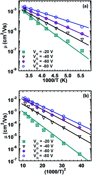 |
| | Fig. 7 Temperature dependence of μ, measured at different VG for CuPc OFETs (a) with and (b) without traps. Solid lines in (a) and (b) represent the fitting according MTR model and PM, respectively.43,48 | |
Anomalous temperature dependence of IDS in OFETs with traps
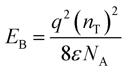
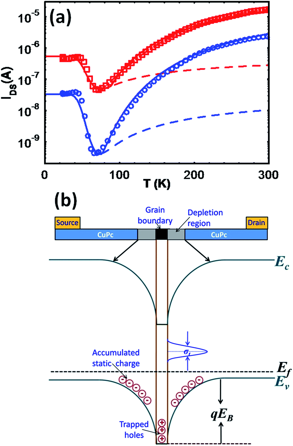
To reveal the nature of traps and their resulting impact on charge carrier transport in disordered organic semiconductors, temperature dependence of IDS at two different VG of 60 V and 90 V for OFETs based on CuPc thin films having traps has been shown in Fig. 8(a). Initially IDS decreases with decreasing temperature but at around 75 K and 65 K for VG = 60 V and 90 V, respectively, magnitude of current increases suddenly by several orders and then remains almost constant. This anomalous behavior in current–temperature (IDS–T) characteristics can be explained on the basis of grain boundary controlled charge carrier transport in CuPc thin film with traps.51 Fig. 8(b) shows the energy-level diagram including band-bending due to the trapping of positive charge at the grain boundary interface in CuPc thin films. High density of localized energy levels inside the band gap of the semiconductor exists due to the interface states lying between grain boundaries in polycrystalline thin films with traps.50,51 The levels which lie below the Fermi level EF, are filled, at thermal equilibrium. Consequently, a negative charge at the interfaces and space-charge regions on the both sides, of grain boundaries are generated. Positive charge, trapped at the grain-boundary interface creates a potential barrier for charge carrier transport and the height of this barrier (EB) can be estimated51,52| |
 | (11) |
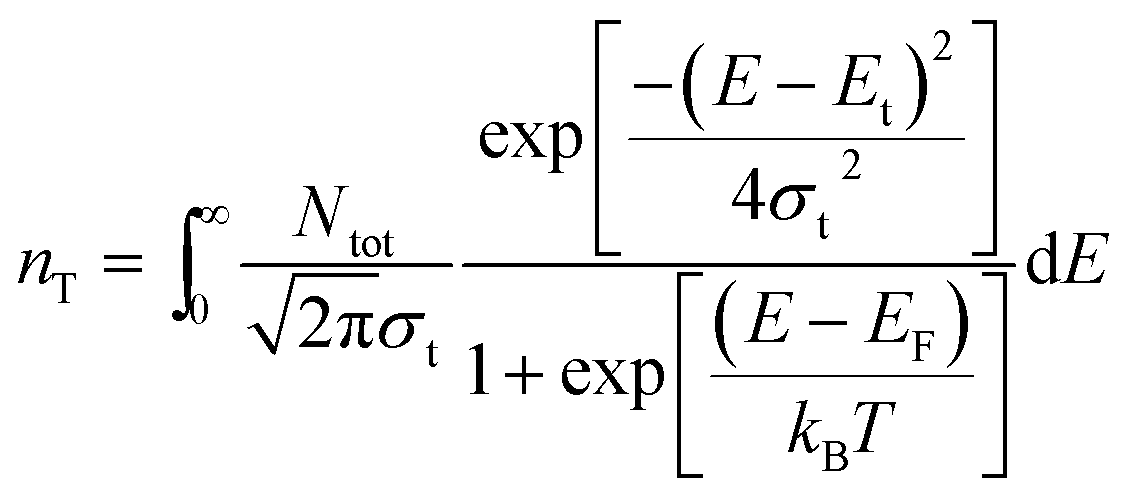
where NA is the acceptor concentration inside the grain, nT is the density of occupied traps at grain boundary interface. nT depends on the Fermi level, hence on T and for a Gaussian distribution of trap in organic semiconductors, can be given by50| |
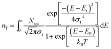 | (12) |
where ET represents the maximum height of the Gaussian distribution. EF is given by| | |
EF(T) = kBTln[NV/p]
| (13) |
IDS, in polycrystalline thin films with large number of grains is controlled by the rate of charge carrier jumps across the grain boundary as53| | |
IDS = I0exp[−(EB + Δ)/kBT]
| (14) |
where Δ is an additional barrier due to hopping conduction. Experimental IDS–T characteristics have been simulated according to the eqn (11)–(14) and results are also presented in Fig. 8(a). It is to be noted that in low temperature region (upto around 75 K and 65 K for VG = 60 V and 90 V, respectively), IDS–T characteristics can be excellently fitted without inclusion of Δ i.e. after putting Δ = 0 in eqn (14). Hence at low temperatures, charge transport in polycrystalline thin films is completely controlled by grain boundaries. However, at high temperature simulation results deviate from experimental one (dashed lines in Fig. 8(a)) because an additional barrier Δ due to hopping conduction also contributes. Hence for temperatures higher than ∼75 K and 65 K for VG = 60 V and 90 V, respectively, Δ has a finite value. After adding Δ to EB, experimental data could be excellently fitted at high temperatures (shown by solid lines in Fig. 8(a)). From fitting Δ has been found to be 82 meV and 43 meV for VG = 60 V and 90 V, respectively.
 |
| | Fig. 8 (a) Temperature dependence of IDS at VG = 60 V (open circle) and VG = 90 V (open square) for OFETs based on CuPc thin films with traps. Abrupt increase in IDS at ∼75 K for VG = 60 V and at ∼65 K for VG = 90 V has been observed. Dashed lines represent the theoretical fitting according to eqn (14), without inclusion of hopping barrier (Δ) i.e. by putting Δ = 0 in eqn (14) whereas solid lines represent the theoretical fitting with a finite value of Δ. (b) The schematic representation of energy-level diagram including band-bending at grain-boundary interface in CuPc thin films. Ec and Ev represent the LUMO and HOMO edges, respectively and EF is the equilibrium Fermi level. | |
Conclusions
In conclusion, we have identified and characterized the traps in polycrystalline organic thin films of CuPc using two and three terminal devices. It has been found that the trap density can be controlled by varying growth conditions and CuPc thin films grown at low substrate temperatures are proved to have large concentration of traps. The presence of traps is analyzed by TCLC in two terminal devices. C–f and C–T characteristics also demonstrate the presence of traps in CuPc thin films grown at low TG. Width of the trap distribution from MTR model is in agreement with that obtained independently from C–f characteristics of CuPc based organic Schottky diodes. Hence MTR model can be applied to the charge carrier transport in polycrystalline organic thin films with isotropic grainy structure. Charge carriers trapped by interface states at grain boundaries cannot hop to HOMO or LUMO unless they get sufficient energy to be released because trapped charges at the grain-boundary interfaces lead to the formation of a potential barrier for charge transport process. Polycrystalline thin films grown under favorable growth conditions to achieve anisotropic morphology with fewer grain boundaries seem to be providing a percolative passage for the carrier transport.
Conflicts of interest
There are no conflicts to declare.
Acknowledgements
V. R. thanks UGC, India, for the financial support through fellow-ship. This work was partly supported by DST, Government of India.
References
- Y. Shen, K. Diest, M. H. Wong, B. R. Hsieh, D. H. Dunlap and G. G. Malliaras, Phys. Rev. B: Condens. Matter Mater. Phys., 2003, 68, 081204 CrossRef.
- S. J. Konezny, M. N. Bussac and L. Zuppiroli, Phys. Rev. B: Condens. Matter Mater. Phys., 2010, 81, 045313 CrossRef.
- H. Sirringhaus, Adv. Mater., 2005, 17, 2411 CrossRef CAS.
- D. Braga and G. Horowitz, Adv. Mater., 2009, 21, 1473 CrossRef CAS.
- P. Kumar, A. Sharma, S. Yadav and S. Ghosh, Org. Electron., 2013, 14, 1663 CrossRef CAS.
- S. Tadayyon, H. Grandin, K. Griffiths, P. Norton, H. Aziz and Z. Popovic, Org. Electron., 2004, 5, 157 CrossRef CAS.
- Y.-S. Hsiao, W.-T. Whang, S.-C. Suen, J.-Y. Shiu and C.-P. Chen, Nanotechnology, 2008, 19, 415603 CrossRef PubMed.
- S. Yadav, P. Kumar and S. Ghosh, Appl. Phys. Lett., 2012, 101, 193307 CrossRef.
- Q. Wei, K. Hashimoto and K. Tajima, ACS Appl. Mater. Interfaces, 2011, 3, 139 CAS.
- R. J. Chesterfield, J. C. McKeen, C. R. Newman, P. C. Ewbank, D. A. d. S. Filho, J. L. Bredas, L. L. Miller, K. R. Mann and C. D. Frisbie, J. Phys. Chem. B, 2004, 108, 19281–19292 CrossRef CAS.
- B. Hartenstein, H. Bässler, A. Jakobs and K. W. Kehr, Phys. Rev. B: Condens. Matter Mater. Phys., 1996, 54, 8574–8579 CrossRef CAS.
- A. Salleo, T. W. Chen, A. R. Völkel, Y. Wu, P. Liu, B. S. Ong and R. A. Street, Phys. Rev. B: Condens. Matter Mater. Phys., 2004, 70, 115311 CrossRef.
- G. Horowitz, Adv. Mater., 1998, 10, 365–377 CrossRef CAS.
- M. C. J. M. Vissenberg and M. Matters, Phys. Rev. B: Condens. Matter Mater. Phys., 1998, 57, 12964–12967 CrossRef CAS.
- R. Hausermann, K. Willa, B. Blulle, T. Morf, A. Facchetti, Z. Chen, J. Lee and B. Batlogg, Org. Electron., 2016, 28, 306–313 CrossRef CAS.
- D. Guo, T. Miyadera, S. Ikeda, T. Shimada and K. Saiki, J. Appl. Phys., 2007, 102, 023706 CrossRef.
- Z. Bao and J. Locklin, Organic field-effect transistors, CRC press, 2007 Search PubMed.
- A. Sharma, P. Kumar, B. Singh, S. R. Chaudhuri and S. Ghosh, Appl. Phys. Lett., 2011, 99, 023301 CrossRef.
- T. P. Nguyen, Phys. Status Solidi A, 2008, 205, 162–166 CrossRef CAS.
- H. Sirringhaus, Adv. Mater., 2009, 21, 3859–3873 CrossRef CAS.
- L. Wang, D. Fine, D. Basu and A. Dodabalapur, J. Appl. Phys., 2007, 101, 054515 CrossRef.
- S. Hirae, M. Hirose and Y. Osaka, J. Appl. Phys., 1980, 51, 1043–1047 CrossRef CAS.
- J. R. Ayres, J. Appl. Phys., 1993, 74, 1787–1792 CrossRef CAS.
- W. Zhu, T. Low, Y.-H. Lee, H. Wang, D. B. Farmer, J. Kong, F. Xia and P. Avouris, Nat. Commun., 2014, 5, 3087 Search PubMed.
- A. K. Mahapatro and S. Ghosh, Appl. Phys. Lett., 2002, 80, 4840–4842 CrossRef CAS.
- S. M. Sze and K. K. Ng, Physics of Semiconductor Devices, Wiley-Interscience, 3rd edn, 2006 Search PubMed.
- Y. Zhihao, et al., Nat. Commun., 2014, 5, 5290 CrossRef PubMed.
- A. Hoshino, Y. Takenaka and H. Miyaji, Acta Crystallogr., Sect. B: Struct. Sci., 2003, 59, 393 Search PubMed.
- B. Ramachandhran, H. G. A. Huizing and R. Coehoorn, Phys. Rev. B: Condens. Matter Mater. Phys., 2006, 73, 233306 CrossRef.
- M. M. Mandoc, B. de Boer and P. W. M. Blom, Phys. Rev. B: Condens. Matter Mater. Phys., 2006, 73, 155205 CrossRef.
- G. Paasch and S. Scheinert, J. Appl. Phys., 2009, 106, 084502 CrossRef.
- D. K. Schroder, Semiconductor Material and Device Characterization, John Wiley & Sons, Inc., Hoboken, New Jersey, 3rd edn, 2006 Search PubMed.
- V. Kumar, S. Jain, A. Kapoor, J. Poortmans and R. Mertens, J. Appl. Phys., 2003, 94, 1283–1285 CrossRef CAS.
- R. Agrawal, P. Kumar, S. Ghosh and A. K. Mahapatro, Appl. Phys. Lett., 2008, 93, 073311 CrossRef.
- M. A. Lampert and P. Mark, Current injection in solids; Electrical science series, Academic Press, 1970 Search PubMed.
- H. Bassler, Phys. Status Solidi B, 1993, 175, 15–56 CrossRef.
- A. Sharma, S. Yadav, P. Kumar, S. Ray Chaudhuri and S. Ghosh, Appl. Phys. Lett., 2013, 102, 143301 CrossRef.
- S. S. Hegedus and E. A. Fagen, J. Appl. Phys., 1992, 71, 5941 CrossRef CAS.
- J. Bhattacharya, R. W. Mayer, M. Samiee and V. L. Dalal, Appl. Phys. Lett., 2012, 100, 193501 CrossRef.
- K. Harada, A. G. Werner, M. Pfeiffer, C. J. Bloom, C. M. Elliott and K. Leo, Phys. Rev. Lett., 2005, 94, 036601 CrossRef CAS PubMed.
- J. Steiger, R. Schmechel and H. von Seggern, Synth. Met., 2002, 129, 1–7 CrossRef CAS.
- W. L. Kalb and B. Batlogg, Phys. Rev. B: Condens. Matter Mater. Phys., 2010, 81, 035327 CrossRef.
- J. A. Letizia, J. Rivnay, A. Facchetti, M. A. Ratner and T. J. Marks, Adv. Funct. Mater., 2010, 20, 50–58 CrossRef CAS.
- P. Kumar, A. Sharma, S. Ray Chaudhuri and S. Ghosh, Appl. Phys. Lett., 2011, 99, 173304 CrossRef.
- A. K. Hailey, S.-Y. Wang, Y. Chen, M. M. Payne, J. E. Anthony, V. Podzorov and Y.-L. Loo, Adv. Funct. Mater., 2015, 25, 5662–5668 CrossRef CAS.
- L. Li, G. Meller and H. Kosina, Synth. Met., 2007, 157, 243–246 CrossRef CAS.
- C. Tanase, E. J. Meijer, P. W. M. Blom and D. M. de Leeuw, Phys. Rev. Lett., 2003, 91, 216601 CrossRef CAS PubMed.
- C. Tanase, P. Blom and D. de Leeuw, Phys. Rev. B: Condens. Matter Mater. Phys., 2004, 70, 193202 CrossRef.
- S. D. Baranovskii, Phys. Status Solidi B, 2014, 251, 487–525 CrossRef CAS.
- S. V. Novikov, D. H. Dunlap, V. M. Kenkre, P. E. Parris and A. V. Vannikov, Phys. Rev. Lett., 1998, 81, 4472–4475 CrossRef CAS.
- A. K. Mahapatro, N. Sarkar and S. Ghosh, Appl. Phys. Lett., 2006, 88, 162110 CrossRef.
- J. W. Orton and M. J. Powell, Rep. Prog. Phys., 2000, 43, 1263–1307 CrossRef.
- S. Verlaak, V. Arkhipov and P. Heremans, Appl. Phys. Lett., 2003, 82, 745–747 CrossRef CAS.
|
| This journal is © The Royal Society of Chemistry 2017 |
Click here to see how this site uses Cookies. View our privacy policy here. 
 Open Access Article
 This Open Access Article is licensed under a
  ,
Akanksha Sharma,
Pramod Kumar,
Budhi Singh and
Subhasis Ghosh*
,
Akanksha Sharma,
Pramod Kumar,
Budhi Singh and
Subhasis Ghosh*


 and Ea is the activation energy, given by