
 Open Access Article
 This Open Access Article is licensed under a
 Creative Commons Attribution 3.0 Unported Licence
Investigation of micro- and nanoscale barrier layer capacitance mechanisms of conductivity in CaCu3Ti4O12 via scanning probe microscopy technique†
M. S. Ivanov *a,
F. Amaral*bc,
V. A. Khomchenkoa,
J. A. Paixãoa and
L. C. Costac
*a,
F. Amaral*bc,
V. A. Khomchenkoa,
J. A. Paixãoa and
L. C. Costac
aCFisUC, Department of Physics, University of Coimbra, P-3004-516 Coimbra, Portugal. E-mail: maxim.ivanov@uc.pt
bCollege of Health Technology of Coimbra, Polytechnic Institute of Coimbra, Coimbra, 3040-162, Portugal. E-mail: filipe.amaral@estescoimbra.pt
cI3N, Physics Department University of Aveiro, 3810-193 Aveiro, Portugal
First published on 21st August 2017
Abstract
In this work we disclose micro- and nanoscale origins of the unusually high dielectric constant characteristic of CaCu3Ti4O12 (CCTO) ceramic by using the Scanning Probe Microscopy (SPM) technique. Two main mechanisms responsible for the colossal dielectric constant specific to the CCTO compound have been revealed. There is a microscale barrier layer capacitance (MBLC) mechanism, attributed to the potential grain-to-grain barriers, and a nanoscale barrier layer capacitance (NBLC) mechanism, attributed to the potential barriers created by the structural defects such as twinning or slip planes. Using the contact spreading resistance mode of SPM, we have found two types of surface morphology which, being originated from planar defects, can be related to the NBLC mechanism. A clear confirmation of NBLC as the origin of the huge dielectric constant in CCTO has been obtained via the local current–voltage dependence measurements. By using this method, we have found the existence of two sources of conductivity (charge transfer and charge hopping) which simultaneously contribute to the NBLC mechanism. These sources (providing semiconducting and n-type conducting behavior, respectively) have been associated with the different stacking faults predicted for CCTO. The present work promotes a general understanding of anomalous colossal dielectric constant behavior in CCTO material at the macro- and nanoscale levels.
Introduction
Dielectrics with colossal dielectric constant (ε > 103) are a matter of great interest since their use as passive components could provide an improvement in the efficiency of electronic devices and ensure the miniaturization of capacitive electronic elements. These materials can find application as high energy-density storage capacitors (usually referred to as supercapacitors), as high-k gate oxides for field-effect transistors or as microwave dielectric resonators, substrates and other microwave elements. Nowadays, only five mechanisms underlying the colossal dielectric constant (CDC) are recognized. Those are ferroelectricity, charge-density wave formation, hopping charge transport, metal-insulation transition and interface effects.1 Most of the capacitive materials that are being used in electronic industry exploits ferroelectricity as the main origin of CDC. Among them, BaTiO3, PbZr1−xTixO3 and Ba1−xSrxTiO3 are the most representative ones. However, this class of materials exhibits a strong temperature dependence of dielectric properties related to the existence of a ferroelectric phase transition. This fact implies some limitations to the application of ferroelectrics as CDC in certain cases.Calcium copper titanate, CaCu3Ti4O12 (CCTO), a non-ferroelectric material, whose exceptional dielectric properties were for the first time reported in 2000,2 attracted the attention of the scientific community because of its CDC (ε > 105), observed both in ceramics and single crystals. Moreover, the absence of ferroelectric transition makes CCTO properties quite stable, with a wide range of temperature-independent dielectric behaviour. However, the manifestation of high dielectric losses (tan![[thin space (1/6-em)]](https://www.rsc.org/images/entities/char_2009.gif) δ > 0.1), particularly for frequencies around the typical Maxwell–Wagner dielectric relaxation (∼MHz) deteriorates the exclusive permittivity properties of CCTO.3 Besides the challenge linked with the optimization of CCTO properties, regarding its possible prospects to applications in electronic devices, a conclusive explanation about the polarization mechanisms that could justify the dielectric behaviour of CDC is still missing. Discarding the existence of any ferroelectric nature due to geometrically frustrated symmetrical off-center displacement of Ti ions, and/or any other lattice contribution,4 the experimental data, collected during the last decade, point out to extrinsic barrier mechanisms as the main origin of the observed dielectric polarization. Sinclair et al.5 admitted the CDC of CCTO to be the result of an electronically heterogeneous microstructure associated with the semiconducting grains having the insulating surfaces formed during the sintering process. These internal barrier layers, formed by the interface grain-to-grain boundary, operate as multiple micro-capacitors, accumulating electric charge at the grain surfaces when an external electric field is applied. This model correctly explains the behaviour of polycrystalline CCTO samples,6,7 but fails to justify the CDC values measured in CCTO single crystals. Alternatively, Krohns et al. proposed the effect of the electrode–sample interface, known as electrode process polarization state.8 This polarization may arise from the depletion layers of Schottky or metal–insulator–semiconductor (MIS) diode structures at the interfaces between the metallic electrodes and the bulk sample.8 Although this effect can occur both in polycrystalline and single crystal CCTO samples, this hypothesis was later discarded. Since the removal of samples surface does not change, as much as expected, the CDC values of the samples, electrode polarization process cannot stand as the main polarization mechanism.9 Other barrier models, valid for poly and single crystals, were firstly suggested by Subramanian et al.10 and further developed by Bueno et al.11 In ref. 10, the plane defect model due to the twinning parallel to the (100), (010), and (001) planes was proposed as a plausible microscopic explanation for the gigantic dielectric constants in CCTO material and the local electronic structure of twinning planes were examined precisely. In ref. 11, this approach was significantly developed and manifested as a polaronic stacking fault defect model. In this model, the stacking faults at the nanoscale level work as a large association of internal barrier layer capacitors, thus resulting in the huge dielectric constant observed in CCTO based materials. This phenomenon was named as nanoscale barrier layer capacitance (NBLC) mechanism and a huge enhancement of polaronic defects was predicted. Later on, Ribeiro et al. showed that the Debye relaxation process appearing in polycrystalline CCTO samples at high frequency had polaronic nature.12
δ > 0.1), particularly for frequencies around the typical Maxwell–Wagner dielectric relaxation (∼MHz) deteriorates the exclusive permittivity properties of CCTO.3 Besides the challenge linked with the optimization of CCTO properties, regarding its possible prospects to applications in electronic devices, a conclusive explanation about the polarization mechanisms that could justify the dielectric behaviour of CDC is still missing. Discarding the existence of any ferroelectric nature due to geometrically frustrated symmetrical off-center displacement of Ti ions, and/or any other lattice contribution,4 the experimental data, collected during the last decade, point out to extrinsic barrier mechanisms as the main origin of the observed dielectric polarization. Sinclair et al.5 admitted the CDC of CCTO to be the result of an electronically heterogeneous microstructure associated with the semiconducting grains having the insulating surfaces formed during the sintering process. These internal barrier layers, formed by the interface grain-to-grain boundary, operate as multiple micro-capacitors, accumulating electric charge at the grain surfaces when an external electric field is applied. This model correctly explains the behaviour of polycrystalline CCTO samples,6,7 but fails to justify the CDC values measured in CCTO single crystals. Alternatively, Krohns et al. proposed the effect of the electrode–sample interface, known as electrode process polarization state.8 This polarization may arise from the depletion layers of Schottky or metal–insulator–semiconductor (MIS) diode structures at the interfaces between the metallic electrodes and the bulk sample.8 Although this effect can occur both in polycrystalline and single crystal CCTO samples, this hypothesis was later discarded. Since the removal of samples surface does not change, as much as expected, the CDC values of the samples, electrode polarization process cannot stand as the main polarization mechanism.9 Other barrier models, valid for poly and single crystals, were firstly suggested by Subramanian et al.10 and further developed by Bueno et al.11 In ref. 10, the plane defect model due to the twinning parallel to the (100), (010), and (001) planes was proposed as a plausible microscopic explanation for the gigantic dielectric constants in CCTO material and the local electronic structure of twinning planes were examined precisely. In ref. 11, this approach was significantly developed and manifested as a polaronic stacking fault defect model. In this model, the stacking faults at the nanoscale level work as a large association of internal barrier layer capacitors, thus resulting in the huge dielectric constant observed in CCTO based materials. This phenomenon was named as nanoscale barrier layer capacitance (NBLC) mechanism and a huge enhancement of polaronic defects was predicted. Later on, Ribeiro et al. showed that the Debye relaxation process appearing in polycrystalline CCTO samples at high frequency had polaronic nature.12
Nevertheless, the conductivity process within the CCTO grains is still an open question. Both electron transfer through polarons11 and localized hopping charge carriers,13 confined within small domains, can explain the conductivity behavior in CCTO ceramics. Two kinds of morphologies were initially identified in polycrystalline CCTO ceramic samples: terraces with ledges and bump domains.14 These structures were observed inside grains after treating the samples at higher etching temperatures and longer etching times (as compared with a conventional preparation procedure). The self-intertwined domain structures inside the grains of the polycrystalline CCTO were investigated in details by scanning electron microscopy (SEM) and high-resolution transmission electron microscopy (HRTEM) in ref. 15. The main origin of the observed morphologies was found to be associated with screw-like dislocations resulting from spiral growth of the crystal.
In this work, we present an experimental confirmation for the inhomogeneous conductivity in CCTO ceramics that is measured at the macro- and nanoscale levels. Two main mechanisms responsible for the colossal dielectric constant behaviour of the CCTO sample were found. There is a microscale barrier layer capacitance (MBLC) mechanism, attributed to the potential grain-to-grain barriers, and a nanoscale barrier layer capacitance (NBLC) mechanism, attributed to the potential barriers, which are created by the structural defects such as twinning or slip planes. An adequate interpretation of the nanoscale dielectric responses based on the appropriate existing models (electrical equivalent circuit containing MBLCs and NBLCs parts) and its comparison with the macroscopic complex impedance experimental data are presented.
Methodology
Synthesis of the sample
Ceramic pellet of CCTO was prepared by a conventional solid state reaction method using the powders of calcium carbonate CaCO3 (Fluka, Honeywell Research, 99%), titanium oxide TiO2 (Sigma-Aldrich, 99%) and copper oxide CuO (Sigma-Aldrich, 99%) taken in stoichiometric cation ratio. The reagents were mixed in a planetary mill during 20 min at 200 rpm, and the mixture was calcinated at 900 °C for 12 h. The calcined powder was grinded using a mortar and a pestle and uniaxially pressed into cylindrical pellets with a diameter of 12 mm and a thickness of 3 mm by applying 1.2 tons load for 5 min. Sintering was performed at 1050 °C for 12 h. The sintering temperature was chosen in agreement with the previous study,6,16 showing the clear benefits of the corresponding temperature range in comparison with other tested temperatures. Grinding and mechanical polishing of the sintered sample was performed using SiC abrasive papers (ranging from 500 to 1200 grits) and diamond paste. To reveal the grain boundaries, the mechanically-polished sample was thermally etched at 950 °C for 1 h.Measurement details
Structural analysis was performed using a Philips X'pert diffractometer with Cu Kα radiation. The X-ray diffraction (XRD) pattern was collected in the angle range 10° ≤ 2θ ≤ 80° with a step of 0.026° and a dwell of 2 s per step. The diffraction data were analyzed by the Le Bail method17 using the FullProf software package.18 The microscale morphology and chemical analysis of the sample were performed using a Hitachi S4100-1 scanning electron microscope (SEM) equipped with an energy-dispersive X-ray spectroscopy (EDS) detector. The dielectric properties of the sample were measured with an Agilent 4294A LCR meter within a frequency range from 40 Hz to 110 MHz. For this measurement, the opposite sides of the samples were painted with silver paste. All the dielectric measurements were done in a homemade cryostatic bath system within the temperature range between 86 and 350 K. The dielectric setup was implemented in Cp–Rp configuration which allows measuring the complex permittivity:| ε*(ω) = ε′(ω) − iε′′(ω), | (1) |
 | (2) |
 | (3) |
Results and discussion
It has been previously reported that CCTO ceramics contain crystal grains whose size can vary in a very broad range.19 Fig. 1(a) illustrates a polished surface of CCTO sample and demonstrates this wide (from 5 μm to 50 μm) grain size distribution. The presence of CuO impurities, as a segregation phase around the CCTO grains, has been revealed by the EDS measurements (Fig. 1(b)). The CCTO is, however, the major phase presented in the sample, as can be seen from the XRD data shown in Fig. 1(c).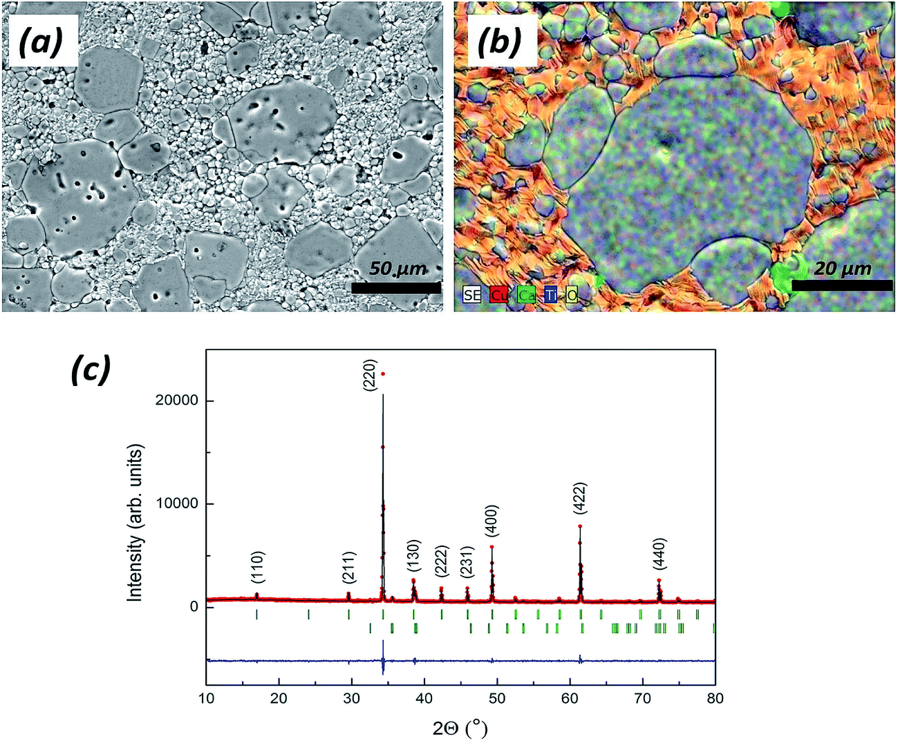 | ||
Fig. 1 Microscopy images of CCTO sample obtained with (a) SEM and (b) EDS mapping. (c) Observed (red symbols), calculated (black line) and difference (blue line) XRD patterns obtained for the CaCu3Ti4O12 sample (a = 7.393(1) Å, space group Im![[3 with combining macron]](https://www.rsc.org/images/entities/char_0033_0304.gif) ) at room temperature. Tick marks indicate the positions of allowed Bragg reflections for the main phase (upper row, the most intensive peaks are indexed) and for the CuO impurity (lower row). ) at room temperature. Tick marks indicate the positions of allowed Bragg reflections for the main phase (upper row, the most intensive peaks are indexed) and for the CuO impurity (lower row). | ||
Fig. 2 presents the real and imaginary parts of the dielectric permittivity spectra. For all the studied temperature range [86–350 K], the dielectric relaxation decays are easily identified through the huge decrease of ε′ followed by an increase of ε′′ which reaches its maximum shifting towards higher frequencies with increasing temperature. The Debye-like dielectric relaxation presents a static dielectric constant (εs), which slightly increases with temperature and reaches 7943 at 90 K. This value is sufficiently high to consider the investigated CCTO sample as a material with colossal dielectric constant. Although the values of ε′ and ε′′ increase in low frequency region (f < 1 kHz) and at temperature above 300 K, this could be explained by the appearance of Jonscher low-frequency dispersion.20 At the low frequency range, the imaginary part of the complex dielectric constant (ε′′) depends on frequency according to Jonscher's power law:
| ε′′ = K(T)ωn−1 | (4) |
f) within the several temperatures (see in Fig. 2(a)) presents the dielectric relaxation peaks at high frequency region which can be associated to the bulk dielectric response. Once this relaxation process is thermally activated, Arrhenius law was used to calculate the activation energies associated with this process. The variation of relaxation frequency (fmax) with temperature is expressed by the equation:| fmax = f0e−Ea/KT | (5) |
fmax as a function of the inverse temperature (1/T) is presented in Fig. 2(b). The analysis of fitting curve and the linearization of eqn (5) gave the activation energy value of 100 ± 2 meV for observed relaxation process. Comparing this result with the literature reporting the activation energy of polaronic relaxation process in more than 50 perovskites,21 we notice an evident proximity of CCTO to the same polaronic relaxation behaviour.
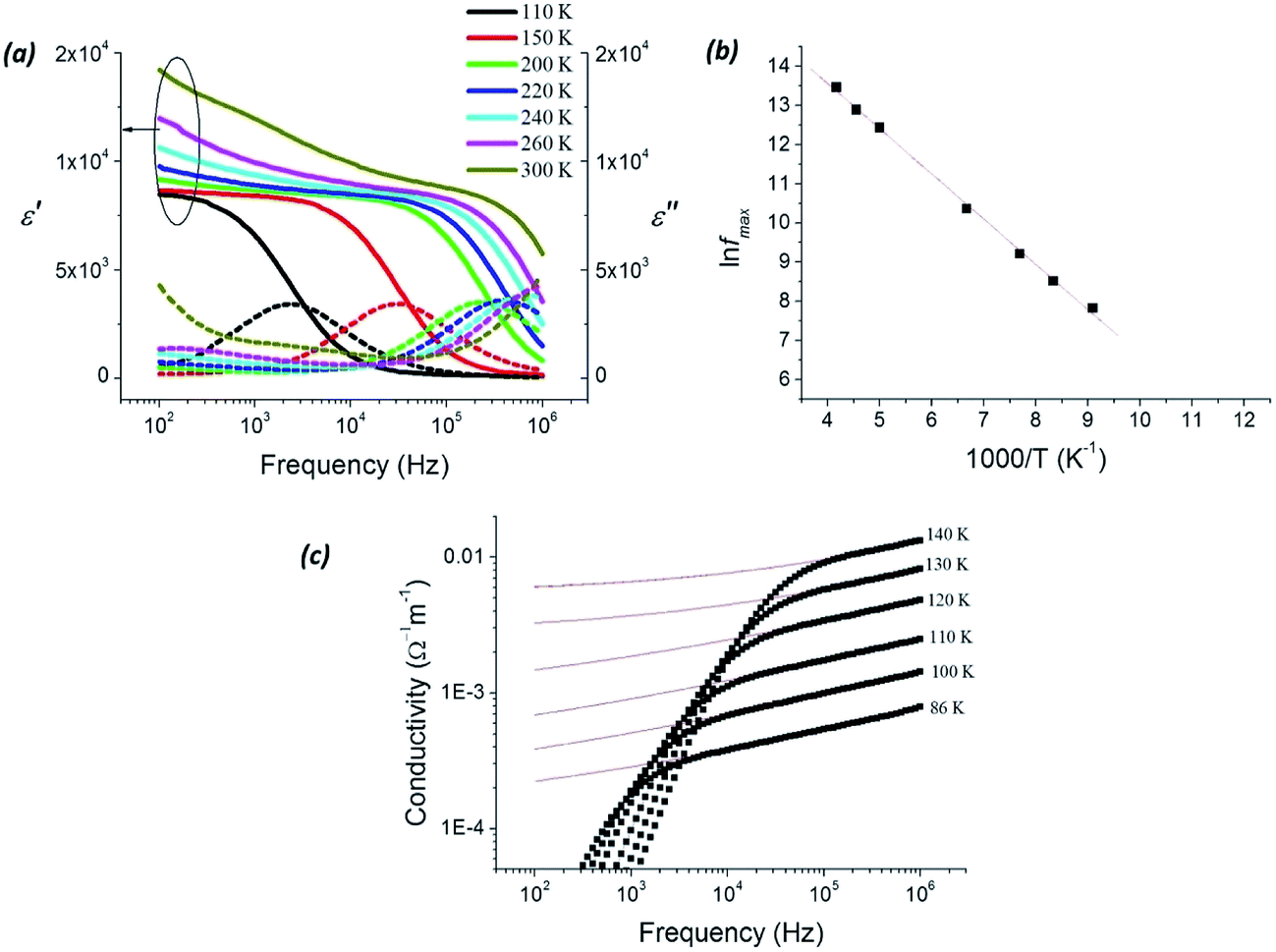 | ||
| Fig. 2 The real and imaginary dielectric permittivity spectra (a), Arrhenius law (b) and universal dielectric response (c) fittings. | ||
The experimental result on conductivity of the sample at high frequencies has also revealed a strong polaronic nature of dielectric permittivity (Fig. 2(c)). Indeed, at low temperature conditions (T < 200 K) and high frequency (f > 1 kHz) the conductivity behaviour of the CCTO sample obeys the Universal Dielectric Response (UDR):20
| σ = σdc + σ0fs | (6) |
| T (K) | σdc (Ω−1 m−1) | σ0 (Ω−1 m−1) | s | Δσdc (Ω−1 m−1) | Δσ0 (Ω−1 m−1) | Δs |
|---|---|---|---|---|---|---|
| 86 | 1.2 × 10⁻⁴ | 4.0 × 10⁻⁵ | 2.0 × 10⁻¹ | 0.2 × 10⁻⁴ | 0.5 × 10⁻⁵ | 0.7 × 10⁻⁴ |
| 100 | 1.7 × 10⁻⁴ | 9.0 × 10⁻⁵ | 1.9 × 10⁻¹ | 0.3 × 10⁻⁴ | 1.0 × 10⁻⁵ | 0.6 × 10⁻⁴ |
| 110 | 2.7 × 10⁻⁴ | 1.8 × 10⁻⁴ | 1.8 × 10⁻¹ | 0.5 × 10⁻⁴ | 0.2 × 10⁻⁴ | 0.6 × 10⁻⁴ |
| 120 | 7.9 × 10⁻⁴ | 2.8 × 10⁻⁴ | 1.9 × 10⁻¹ | 0.3 × 10⁻⁴ | 0.9 × 10⁻⁵ | 0.2 × 10⁻⁴ |
| 130 | 2.7 × 10⁻³ | 1.8 × 10⁻⁴ | 2.5 × 10⁻¹ | 0.9 × 10⁻⁴ | 0.2 × 10⁻⁴ | 0.5 × 10⁻⁴ |
| 140 | 5.4 × 10⁻³ | 1.8 × 10⁻⁴ | 2.7 × 10⁻¹ | 0.4 × 10⁻³ | 0.4 × 10⁻⁴ | 0.1 × 10⁻³ |
The employment of scanning probe microscopy technique implemented in contact atomic force microscopy and spreading resistance microscopy modes allowed the analysis of CDC phenomena at the micro- and nanoscale levels to be performed. The AFM study of the surface morphology (Fig. 3(a)) revealed a broad (ranging from 5 μm to 50 μm) grain size distribution, thus confirming the data obtained with the SEM technique (Fig. 1(a)). The current distribution correlates with topography and a clear difference between the grains and grain boundaries can be seen (Fig. 3(b)). These results are consistent with the so-called macroscale barrier layer capacitance (MBLC) mechanism of conductivity described in details in ref. 5 and 6. The MBLC mechanism is considered as controlling the conductivity behavior at the macroscale level. It is known as the main origin of CDC in CCTO materials.5–9 In agreement with the predictions given in ref. 5 and the measurements carried out in ref. 6, we revealed, by using the SPM technique, the higher concentration of charge carriers near the grain boundaries (Fig. 3(b)). This effect has been described in details by Sinclair et al.,5 which showed that during the sintering process the semiconductive grains partially oxidized and the insulating grain boundaries were formed. This phenomenon causes the arising of Schottky type barriers acting as an association of multiple micro-capacitors and resulting in electric charge carrier accumulation. Thus, in this work we show, for the first time, the evidence of the charge accumulation states near the CCTO grain boundaries which were measured experimentally at the microscale level (see Fig. 3(c and d)). The current distribution scan image within the two grains illustrates the MBLC mechanism and its conductivity pattern, including charge carriers' accumulation states at grain boundaries and insulating gap between them. An average width for the insulating gap between the grains is around 5 μm with a depth of around 500 nm. The mean current drop between the conductive and insulating states attains 0.5 nA (Fig. 3(d)).
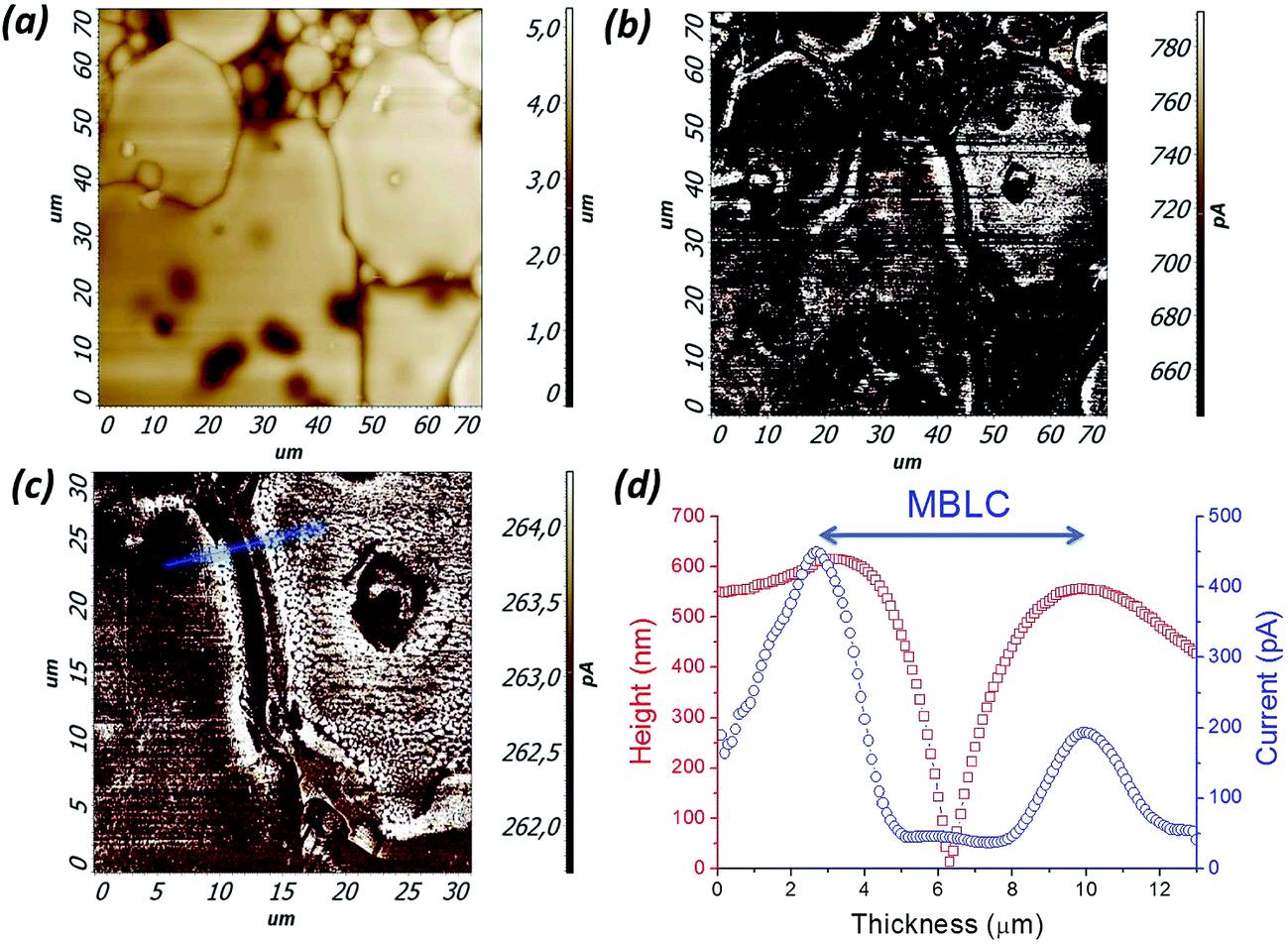 | ||
| Fig. 3 (a) Surface topography, (b and c) spreading resistance scan images and (d) MBLC height and current profiles. The scanning was done at 0.1 Hz (512 × 512 pixels) and dc bias voltage of 1 V. | ||
However, the MBLC mechanism seems not to be solely responsible for CDC properties in CCTO ceramics. The additional mechanism should originate from the existence of an insulating/conductive mesh inside CCTO grains, as can be seen from Fig. 3(c). As the scan resolution is increased, the complex topography of separate CCTO grain becomes seen (Fig. 4(a)). It has been previously reported14,15 that there are two types of surface morphologies which could be found on the surface of CCTO by using the scanning electron microscopy (SEM) and high-resolution transmission electron microscopy (HRTEM) techniques. There are terrace-ledge and bump domain morphologies associated with the spiral growth of crystals via a screw dislocation. In our research we confirm the coexistence of these morphologies via the contact AFM measurements (Fig. 4(a), Fig. 3-ESI†) and describe the bump domains (in our work we named it as “a mesh-type morphology”) as also composed of terrace-ledge domains. It has been suggested14 that grain morphology in CCTO is strongly affected by synthesis conditions. It has been pointed out that the increase in sintering time suppresses the terrace-ledge morphology and promotes changes in the state of the spiral growth dislocations.14 Moreover, it has been shown that the terrace-ledge morphology appears only under thermal etching.14 All these conditions are expected to cause a huge difference in the conductivity behavior of the areas associated with the different morphological types. In the current work we present the experimental evidence for this prediction by using the contact spreading resistance mode measurements.
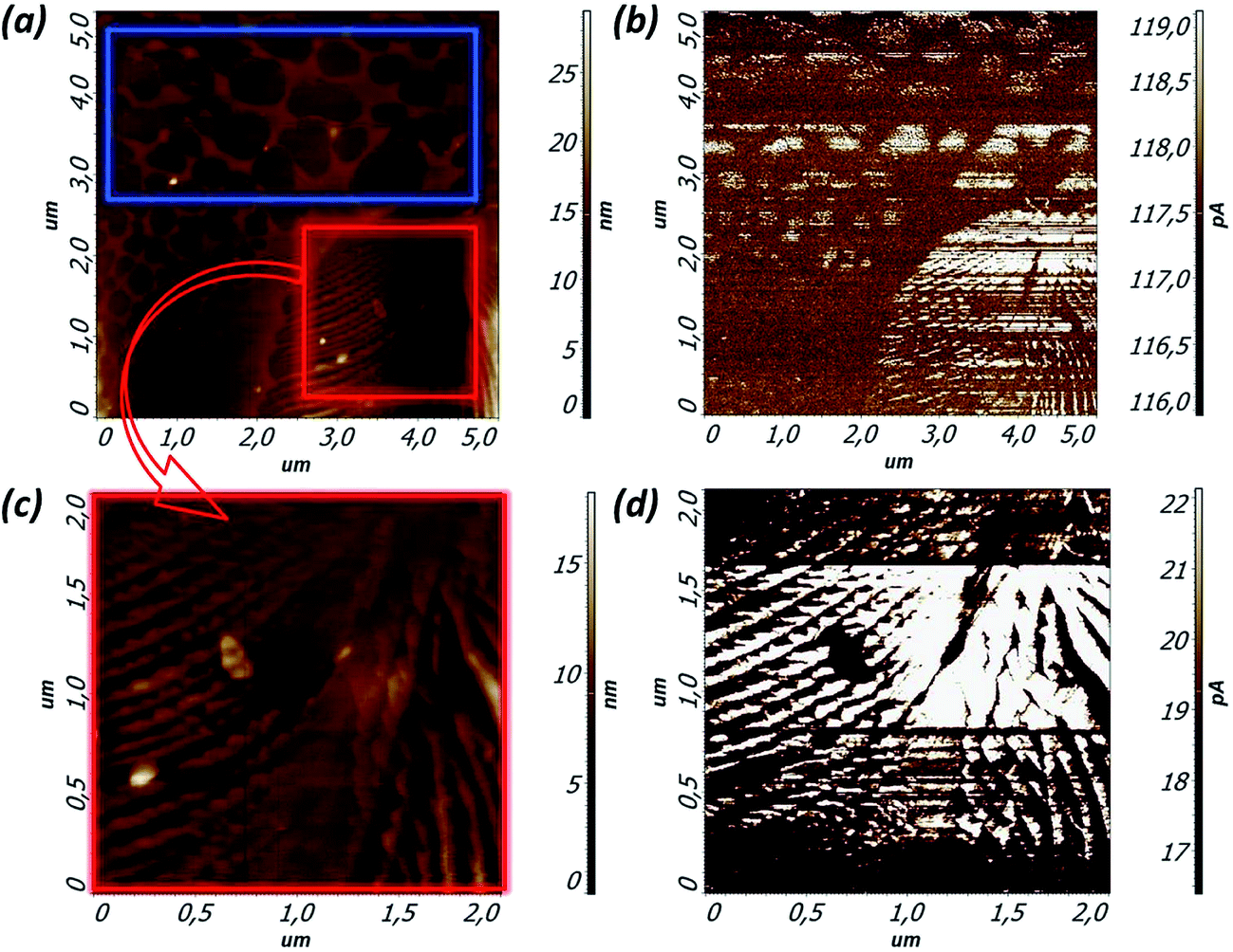 | ||
| Fig. 4 (a, c) Surface topography and (b, d) spreading resistance scan images for terrace-ledge (red square) and mesh type (blue rectangle) morphology areas of CCTO sample. The scanning was done at 0.1 Hz (512 × 512 pixels) and dc bias voltage of 1 V. | ||
As can be seen from Fig. 4(b), the current distribution matches with the topography scan image and presents a clear mapping of conductive behavior for different type of surface morphologies. A precise scan of terrace-ledge domain area was done at the region limited by a red square (see in Fig. 4(a)). The results of morphology and current distribution scans are presented in Fig. 4(c and d). As follows from the scan image analysis, the terrace-ledge domain area represents an alternation of barriers and gaps in topography image scan which correspond to the conductive and insulating stripes in current distribution image scan. An average width and height of the barriers were 100 nm and 2 nm, respectively. The corresponding current, when a dc bias voltage of 5 V was applied, was about 10 nA. Based on the previous theoretical predictions10,11 and some indirect measurements,11–15 we claim the direct evidence for the nanoscale barrier layer capacitance (NBLC) mechanism of conductivity.
Generally, the theory of NBLC mechanism is based on collective effect of negatively charged TiO5 clusters of the stacking fault substructure, which forms a polaronic defect with neighboring Cu2+ atoms.10 Moreover, it has been predicted that these defects are the most likely reason for the maintenance of the high dielectric constant at the high frequency, up to the MHz range.20 It has been shown12–15 that the conductive properties within the grains of polycrystalline CCTO are dependent on both nanoscale internal barriers and electronic conduction paths. This model has been discussed by considering a configuration that gathers conduction barrier and insulating polaronic plane.11,12 In the present work we confirm this prediction via the direct visualization of dual conductivity behavior of CCTO grain at the nanoscale level, which demonstrates the existence of conductive barriers and insulating gaps (polaronic plane). Thus, the results obtained in this work represent the first direct assessment of the NBLC electrical response, performed at the nanoscale level.
A precise scan of mesh type morphology area is presented in Fig. 5(a), where the coexistence of bump and terrace-ledge domains can be seen. However, only the terrace-ledge domain area was found to be conductive, as follows from the current distribution image scan (Fig. 5(b)). The detailed scan of terrace-ledge domain area, included in the mesh type morphology, is presented in Fig. 5(c). A clear contribution of NBLC mechanism associated with the alternation of conductive barriers and insulating gaps was revealed (Fig. 5(d)). An average width and height of the barriers were 200 nm and 2 nm, respectively. These results are quite similar to those obtained for the area shown in Fig. 4(c and d). However, the corresponding current behavior is dramatically different from that observed for the previously studied terrace-ledge morphology area. To distinguish the difference between the terrace-ledge domains, we denote those unrelated to the mesh type morphology as “terrace-ledge 1” (Fig. 4(a and c)) and those related to the mesh type morphology as “terrace-ledge 2” (Fig. 5(a and c)).
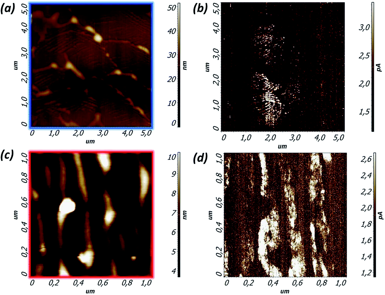 | ||
| Fig. 5 (a, c) Surface topography and (b, d) spreading resistance scan images for terrace-ledge domains embedded into the mesh type morphology area of CCTO sample. The scanning was done at 0.1 Hz (512 × 512 pixels) and dc bias voltage of 1 V. | ||
We consider that the alternate conductive barriers and insulating gaps that appear in both terrace-ledge and mesh type morphology areas have the same origin – the NBLC mechanism. The point is that there is a noticeable difference between them, as clearly revealed by the dissimilar conductivity behavior. The comparison of the two morphology areas demonstrates that when 1 V dc bias voltage is applied, a mean current response of 22 pA (Fig. 4(d)) and 2.6 pA (Fig. 5(d)) is measured for the terrace-ledge 1 and terrace-ledge 2 domains, respectively. Another difference appears in the mean width (100 nm vs. 200 nm) of conductive barriers for terrace-ledge 1 and terrace-ledge 2 domains (Fig. 6(a and b)).
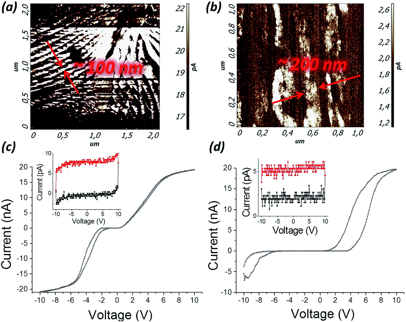 | ||
| Fig. 6 Spreading resistance scan images for (a) terrace-ledge 1 and (b) terrace-ledge 2 domains of CCTO sample. Current–voltage dependences obtained on conductive part of (c) terrace-ledge 1 and (d) terrace-ledge 2 domains of CCTO sample. Inserts show the I–V measurements performed on insulating parts. | ||
The origin of the difference in the conductivity behavior has been investigated via the local current–voltage measurements. The I–V curves have been obtained on conductive and insulating parts of NBLC structure in order to reveal the maximum current intensity and conductivity type. The current measurements on conductive barriers within the terrace-ledge 1 domain reveal a typical semiconductor I–V dependence (which is partly influenced by the Schottky contact) with the threshold voltage of 1 V and −2 V and the saturation voltage of around ±8 V (Fig. 6(c)). The I–V measurements performed on the insulating gap revealed a low current value of about 8 pA, when a 10 V dc bias voltage was applied (inset in Fig. 6(c)). On the contrary, the current–voltage measurements carried out on the terrace-ledge 2 domain structure embedded into the mesh type morphology area demonstrate another type of I–V curve. For this current–voltage dependence we assume that the conductivity behavior should be affected by both the Schottky and n-type semiconductor mechanisms. The n-type conductivity behavior was, for the first time, described in ref. 22, reporting on a clear n-type nature of the CCTO grains and ref. 23, suggesting that the majority of charge carriers in the explored area are electrons and that the main mechanism of conductivity is electron hopping. Thus, n-type conductivity behaviour with the threshold voltage of 2 V and −7 V and the saturation voltage exceeding ±10 V was detected (Fig. 6(d)). The hysteresis in the current–voltage curves is linked with the diode-like rectifying I–V characteristic, indicating a forward pass diode behaviour and a reverse diode behaviour for a backward sweep (similar to that observed in the ref. 24). It can be seen that during the measuring cycle the diode polarity can be switched in the range of 4–6 V. The I–V curve measurements for insulating gap found a low current value of about 6 pA when a 10 V dc bias voltage was applied (insert at Fig. 6(d)). Thus, we claim that the mechanism of conductivity inside the CCTO grains could be successfully described in the framework of NBLC model, but the coexistence of different-type morphology areas with the dissimilar conductivity behaviour should be taken into account.
It is worth to emphasize that the average MBLC and NBLC gap widths in the CCTO ceramics reach 5 μm and 200 nm, respectively. These are approximately 170 and 7 times larger than the Pt/Ir-coated tip apex (∼30 nm) (Fig. 4-ESI†). Moreover, not all terrace-ledge domains demonstrate a correlation between the topography and SR signal (see the cross-sections in Fig. 5-ESI†). Taking into account the small topography roughness as well as the scanning parameters described above (i.e. the large setpoint, high cantilever stiffness and low scanning rate) we consider that we maintain a permanent tight tip-surface contact during the scanning. Accordingly, we believe that our measurements adequately reflect the MBLC and NLBC mechanisms proposed. In order to confirm the origin of the SR signal and exclude the possibility that the observed effects are solely determined by the reduction in contact area at step edges, we repeated the experiments at different scan directions (Fig. 6-ESI†).
Our research is based on the phenomenology considering that the observed CDC behavior in CCTO material requires the coexistence of conductive barriers and insulating gaps caused by the twin boundaries, planar defects and slip planes within the crystallographic structure of the sample. In general, this approach has been initially proposed in ref. 9 and significantly developed in ref. 10 and 11 to yield the structural model for planar defects. Following this model, the ideal arrangement of a perfect crystal of CCTO, where the CuO4 square planes containing Cu2+ ions share corners with the TiO6 octahedra containing Ti4+ ions, could be disrupted as a result of twinning in a CCTO crystal.10–12 This disturbance may create the plane defects and make the Cu and Ti environments conductive by accommodating Cu+ and Ti3+ ions. Simultaneously, it creates the insulating barrier because of the associated charge balance which requires the existence of oxygen vacancies in the defect plane.10 Accordingly, we consider that the observed terrace-ledge 1 domain structure is originated from the twinning or slip planes against the [100] direction along the (220) plane, which is fully consistent with the previous reports.10–15 This sliding motion of one atomic plane by half unit cell – a stacking fault – can explain the dielectric and semiconducting properties of polycrystalline CCTO sample. Indeed, the main conductivity mechanism along the stacking fault ((220) plane) is an electron transfer between TiO5 cluster and Cu2+-containing adjacent structure.10–12
Another scenario is likely realized for the mesh type morphology areas, in which the terrace-ledge domains have increased barriers width and exhibit the change in the conductivity behavior. In accordance with the theoretical predictions given in ref. 10, one of the possible mechanisms for the observed phenomena could be the stacking faults that come from a twinning or slip planes against the [100] direction along the {110} planes. This consideration is generally consistent with the assumption of oxygen vacancies increasing in order to reach higher stability in group of four adjacent TiO5 square pyramids that become connected to the four O atoms of a CuO4 square plane to form four slightly distorted TiO6 octahedra.10 Therefore, the local charge neutrality would be kept by the reduction of Cu2+ to Cu1+ and the formation of oxygen vacancies. This kind of stacking fault makes the electron hopping to be the main mechanism of conductivity in such distorted structure.12,22,23 Finally, this results in n-type conductivity.
Taking into consideration the results obtained, we can construct a principle scheme explaining the conductivity behavior in polycrystalline CCTO sample (Fig. 7 (a); the spreading resistance mode is known as a surface technique (the current flows between the SPM probe and the clamping contact located on a sample surface), so only the surface current distribution was measured). This scheme represents the main mechanisms involved in CDC behavior of CCTO. Those are microscale barrier layer capacitance (MBLC) mechanism, which depends on potential grain-to-grain barriers, and nanoscale barrier layer capacitance (NBLC) mechanism, which depends on potential barriers that are created by structural defects such as twinning or slip planes. We believe that NBLC mechanism is associated with the existence of a number of intertwined domain structures which causes the alternation of conductive and insulating parts. The number of distinct intertwined domain structures should be dependent on possible disruption plane combination. It has been predicted that there should be several possibilities for plane defect along {110} planes resulting from a twinning parallel to the (100), (010), and (001) planes.10–12 In the current work we found two of them distinguished by the conductivity type.
 | ||
| Fig. 7 The principle scheme for (a) general case and (c) measured polycrystalline CCTO sample. (b) The real and imaginary impedance spectra. | ||
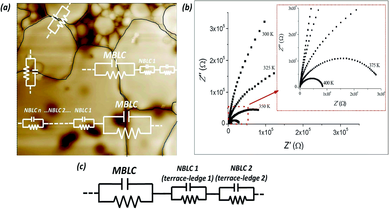
In accordance with the mechanisms proposed, we are able to construct a principle local electric scheme for the CCTO sample (Fig. 7(c)), where the MBLC is defined uniquely (see Fig. 3(c and d)) and the NBLC consists of two components associated with terrace-ledge 1 (Fig. 6(a)) and terrace-ledge 2 (Fig. 6(b)) domains. The calculated from the I–V curve values for the MBLC and NBLC-related impedance (ZMBLC ∼ 10 GΩ, ZNBLC1 ∼ 40 GΩ and ZNBLC2 ∼ 250 GΩ) demonstrate that the global impedance Z = (ZMBLC + ZNBLC1 + ZNBLC2) × S normalized on the scan area factor (S ∼ 10−6) is about 0.3 MΩ. This value is consistent with macroscopic complex impedance data presented in Fig. 7(b). Consequently, this result shows that the impedance is mainly determined by the NBLC mechanism of conductivity.
Conclusions
To sum up, we proposed the direct experimental evidence for MBLC mechanism attributable to potential grain-to-grain barriers and NBLC mechanism associated with potential barriers created by structural defects such as twinning or slip planes. The SPM study allowed two distinct types of surface morphology related to the NBLC mechanism of conductivity to be discovered. These terrace-ledge 1 and terrace-ledge 2 domains have obvious structural difference underlying the change in the conductivity mechanism from electron transfer to electron hopping. We believe that results obtained contribute to general understanding of anomalous CDC behavior in CCTO and related materials.Conflicts of interest
There are no conflicts of interest to declare.Acknowledgements
This work was supported by funds from FEDER (COMPETE 2020 Programme) and FCT-Portuguese Foundation for Science and Technology under the projects UID/CTM/50025/2013 and UID/FIS/04564/2016. M. S. I. is grateful to the Fundaçao para a Ciencia e Tecnologia (FCT) for financial support through the project “MATIS – Materiais e Tecnologias Industriais Sustentáveis (CENTRO-01-0145-FEDER-000014). V. A. K. is grateful to FCT for financial support through the FCT Investigator Programme (project IF/00819/2014/CP1223/CT0011). The authors are grateful to Dr A. L. Kholkin (University of Aveiro) for access to SPM facility.References
- P. Lunkenheimer, S. Krohns and S. Riegg, et al., Colossal dielectric constants in transition-metal oxides, Eur. Phys. J.: Spec. Top., 2009, 61, 61–89 CrossRef.
- A. P. Ramirez, M. A. Subramanian and M. Gardel, et al., Giant dielectric constant response in a copper-titanate, Solid State Commun., 2004, 115, 217–220 CrossRef.
- A. R. West, T. B. Adams and F. D. Morrison, et al., Novel high capacitance materials: BaTiO3: La and CaCu3Ti4O12, J. Eur. Ceram. Soc., 2004, 24, 1439–1448 CrossRef CAS.
- L. He, J. B. Neaton and M. H. Cohen, et al., First-principles study of the structure and lattice dielectric response of CaCu3Ti4O12, Phys. Rev. B, 2002, 65, 214112 CrossRef.
- D. C. Sinclair, T. B. Adams and F. D. Morrison, et al., CaCu3Ti4O12: One-step internal barrier layer capacitor, Appl. Phys. Lett., 2002, 80, 2153 CrossRef CAS.
- R. Schmidt, M. C. Stennett and N. C. Hyatt, et al., Effects of sintering temperature on the internal barrier layer capacitor (IBLC) structure in CaCu3Ti4O12 (CCTO) ceramics, J. Eur. Ceram. Soc., 2012, 32, 3313–3323 CrossRef CAS.
- S. I. R. Costa, M. Li and J. R. Fradeb, et al., Modulus spectroscopy of CaCu3Ti4O12 ceramics: clues to the internal barrier layer capacitance mechanism, RSC Adv., 2013, 3, 7030–7036 RSC.
- S. Krohns, P. Lunkenheimer and S. G. Ebbinghause, et al., Colossal dielectric constants in single-crystalline and ceramic CaCu3Ti4O12 investigated by broadband dielectric spectroscopy, J. Appl. Phys., 2008, 103, 084107–084109 CrossRef.
- M. Li, Z. Shen and M. Nygren, et al., Origin(s) of the Apparent High Permittivity in CaCu3Ti4O12 Ceramics: Clarification on the Contributions from Internal Barrier Layer Capacitor and Sample-Electrode Contact Effects, J. Appl. Phys., 2009, 106, 104106–104108 CrossRef.
- M.-H. Whangbo and M. A. Subramanian, Structural Model of Planar Defects in CaCu3Ti4O12 Exhibiting a Giant Dielectric Constant, Chem. Mater., 2006, 18, 3257–3260 CrossRef CAS.
- P. R. Bueno, R. Tararan and R. Parra, et al., A polaronic stacking fault defect model for CaCu3Ti4O12 material: an approach for the origin of the huge dielectric constant and semiconducting coexistent features, J. Phys. D: Appl. Phys., 2009, 42, 055404–055413 CrossRef.
- W. C. Ribeiro, E. Joanni and R. Savu, et al., Nanoscale effects and polaronic relaxation in CaCu3Ti4O12 compounds, Solid State Commun., 2011, 151, 173–176 CrossRef CAS.
- A. Tselev, C. M. Brooks and S. M. Anlage, et al., Evidence for power-law frequency dependence of intrinsic dielectric response in the CaCu3Ti4O12, Phys. Rev. B, 2004, 70, 144101 CrossRef.
- T. Fang and H.-K. Shiau, Mechanism for Developing the Boundary Barrier Layers of CaCu3Ti4O12, J. Am. Ceram. Soc., 2004, 87, 2072–2079 CrossRef CAS.
- T.-T. Fang and C. P. Liu, Evidence of the Internal Domains for Inducing the Anomalously High Dielectric Constant of CaCu3Ti4O12, Chem. Mater., 2005, 17, 5167–5171 CrossRef CAS.
- F. Amaral, C. P. L. Rubinger and M. A. Valente, et al., Enhanced dielectric response of GeO2-doped CaCu3Ti4O12 ceramics, J. Appl. Phys., 2009, 105, 3 CrossRef.
- A. Le Bail, H. Duroy and J. L. Fourquet, Ab initio structure determination of LiSbWO8 by X-ray powder diffraction, Mater. Res. Bull., 1988, 23, 447–452 CrossRef CAS.
- J. Rodríguez-Carvajal, Recent advances in magnetic structure determination by neutron powder diffraction, Phys. B, 1993, 192, 55–69 CrossRef.
- A. F. L. Almeida, P. B. A. Fevhine and J. C. Goes, et al., Dielectric properties of BaTiO3 (BTO)-CaCu3Ti4O12 (CCTO) composite screen-printed thick films for high dielectric constant devices in the medium frequency (MF) range, Mater. Sci. Eng., B, 2004, 111–113 Search PubMed.
- A. K. Jonscher, Dielectric relaxation in solids, J. Phys. D: Appl. Phys., 1999, 32, R57 CrossRef CAS.
- O. Bidault, M. Maglione and M. Actis, et al., Polaronic relaxation in perovskites, Phys. Rev. B, 1995, 52, 4191 CrossRef CAS.
- S.-Y. Chung, I.-D. Kim and S.-J. L. Kang, Strong nonlinear current–voltage behaviour in perovskite-derivative calcium copper titanate, Nat. Mater., 2004, 3, 774–778 CrossRef CAS PubMed.
- L. Zhang and Z.-J. Tang, Polaron relaxation and variable-range-hopping conductivity in the giant-dielectric-constant material CaCu3Ti4O12, Phys. Rev. B, 2004, 70, 174306 CrossRef.
- M. Salimian, M. Ivanov, F. L. Deepak, D. Y. Petrovykh, I. Bdikin, M. Ferro, A. Kholkin, E. Titus and G. Goncalves, Synthesis and characterization of reduced graphene oxide/spiky nickel nanocomposite for nanoelectronic applications, J. Mater. Chem. C, 2015, 3, 11516–11523 RSC.
Footnote |
| † Electronic supplementary information (ESI) available. See DOI: 10.1039/c7ra06385g |
| This journal is © The Royal Society of Chemistry 2017 |