DOI:
10.1039/C7RA05341J
(Paper)
RSC Adv., 2017,
7, 39666-39675
Porous silicon filled with Pd/WO3–ZnO composite thin film for enhanced H2 gas-sensing performance†
Received
11th May 2017
, Accepted 8th August 2017
First published on 14th August 2017
Abstract
Here, pure ZnO, WO3 and Pd/WO3–ZnO composite porous thin films were successfully synthesized directly on porous silicon by a reactive DC magnetron sputtering technique. A sensor based on the Pd/WO3–ZnO composite porous thin films showed remarkably improved H2 sensing performance with good stability and excellent selectivity compared to that of pure WO3 and ZnO, at a relatively lower operating temperature (200 °C) and with a low detection range of 10–1000 ppm. The enhanced response can be attributed to the heterojunction formed between two dissimilar materials. The underlying mechanism behind their good performance for H2 gas was discussed in detail.
1. Introduction
Hydrogen has been regarded as one of the most promising clean energy sources bearing in mind the zero emission energy fuel and high heat of combustion (142 kJ g−1), producing water without any harmful by-products.1–3 Therefore, the globally growing demand for clean energy has engaged widespread research in the field of H2 as a future renewable energy resource.4–7 Nevertheless, hydrogen is colorless, tasteless and odorless with a low ignition energy (0.02 mJ), high diffusion coefficient (0.60 cm2 s−1) and broad flammable range (4–75%) in air which hinders its convenient application.8–10 Thus, there is an urgent need to realize a reliable, inexpensive and fast response sensor device to detect trace amounts of hydrogen just before the explosive limit, even at low temperature.
Over the past few years, due to human demand, a huge number of materials have been extensively studied and implemented as promising sensing materials to this end. Among the various types of gas sensors, metal oxide semiconductor (MOS) based nanostructured chemiresistive gas sensors have grasped a significant position due to several attractive features such as low cost, simple fabrication, environmental benignity, high sensitivity and selectivity, industrial emission control, biomedical, household security and good compatibility towards microelectronic processes for long range of operations.11–15 Therefore, the chemiresistive gas sensors have attracted a notable attention of the researchers and become most enthusiastic research area among the scientific community since 1980s. In the present time, the developing nanotechnology promises incredible improvement in the sensor designing and capabilities. The main objective of this work is to fabricate the nanostructured composite metal oxide based H2 gas sensors under low detection limit in our environment. Among the other MOSs, WO3 and ZnO as gas sensing materials offer the promising platform towards the oxidizing as well as reducing gases. Generally, the MOS gas sensors need to be operated at relatively high temperatures (350 °C or higher).16,17 Wongchoosuk et al. fabricated a WO3 based sensor to detect hydrogen at 350 °C.18 Therefore, the main emphasis of modern research is on reducing the working temperature of the gas sensors to meet the demand of low power consumption, safety and several industrial applications. Therefore, remarkable efforts have been done to moderate the working temperature (≤200 °C) of gas sensors via formation of (n–n or n–p heterojunction at the interface) nanostructured composite material and enlightening the sensing properties by rising the adsorption and desorption rate of analyte gas molecules at the sensor surface.19,20 This leads to fabrication of the new active sensing material in order to meet the remarkable high sensing performance criteria with fast response, low power consumption, high reproducibility and reliability. Based on these investigations, the Pd decorated WO3–ZnO composite thin films may be fabricated as fast response gas sensors which can be recognized to detect low concentration (ppm) of hydrogen in storage and sensing device applications. Among the various approaches, reactive DC sputtering has been considered as an effective technique for the fabrication of high quality contamination free, highly uniform and stoichiometric growth of the composite nanostructures.21
For chemiresistive gas sensors, the sensing mechanism strongly depends on the change in the resistance caused by strong adsorption and effective diffusion of the analyte gas molecules exposed over the top surface of nanostructured composite materials.10,22 Recently, the performance of the gas sensor predominantly depends on various factors such as the surface morphology, crystal structure, composition of the sensing material, porosity and exposed surface area.23,24 Therefore, the synthesis of nanostructured materials having large surface area with high porosity has been attributed to explore and innovate the new functional materials for highly sensitive and fast response gas sensors.25,26
In the present work, we demonstrated the highly porous bare ZnO, WO3 and Pd/WO3–ZnO composite sensors on the hydrophobic porous silicon substrates fabricated by reactive magnetron DC sputtering technique. Herein, the hydrogen sensing properties of prepared ZnO, WO3 and Pd/WO3–ZnO composite microspheres for an working temperature range of (30–350 °C) under the low detection limit (10–1000 ppm) have been studied in detail. Furthermore, we have studied the variation in the response for hydrogen under several humidity conditions (0–90% RH) at the optimum temperature (200 °C). In addition, we expect that the role of hydrophobic nature of porous silicon substrate established the drastic improvement in stability and recovery process towards H2 sensing thin films. Therefore, this work may provide a new insight into gas sensing mechanism and opens up a promising way to fabricate the low temperature gas sensors.27
2. Experimental
2.1 Materials and chemicals
Tungsten (W) and zinc (Zn) targets of (2′′ diameter, 5 mm thickness) with high purity (99.99%) were purchased from (Testbourne Ltd. UK). The hydrofluoric acid (48%) and ethanol solution were obtained from Merck, India. The p-type (100) oriented silicon wafers (0.68 mm thick, 15–20 Ω cm) were purchased from Bayville Chem, USA.
2.2 Sensor fabrication
The synthesis of porous silicon (PS) substrates was already discussed in authors' previous study.28 Porous silicon can be formed either nanoporous or macroporous structures depending on the formation parameters and the forming solution. It's usually different structures exhibit very high surface to volume ratio, ease of fabrication and compatibility to silicon IC technology leading to smart sensors have been fascinating the researchers worldwide for more than a decade.29,30 Macroporous silicon is one of the most promising candidate for the fabrication of numerous gas sensors.31,32 Herein, we fabricate the porous silicon using electrochemical anodization and it significantly enhance the active surface area for adsorption of analyte gas molecules.33,34 The porous silicon substrates provide the base for the composite material to grow in dome like shape and helps to trap the gas molecules between the gaps. This leads to high sensitivity of the sensing device. After anodization, the fabrication process of sensing material was systematically carried out in a custom designed (12′′ diameter) sputtering chamber (Excel Instruments) using high purity (99.99%) W, Zn and Pd sputter targets (2′′ diameter, 5 mm thick). Prior to deposition, the prepared PS substrates were rinsed in deionized water and kept inside the chamber at fix distance of 6 cm from the W and Zn targets. The bare ZnO, WO3 and Pd decorated WO3–ZnO composite samples were sputtered on the porous silicon substrates using reactive DC magnetron sputtering technique. During all depositions, the synthesis temperature, pressure and time were maintained at room temperature, 10 mTorr and 45 minutes respectively, with continuous flow of high purity (99.99%) Ar![[thin space (1/6-em)]](https://www.rsc.org/images/entities/char_2009.gif) :O2 (4:1) using mass flow controller (MKS). Firstly, the bare WO3 and ZnO thin films were fabricated on porous silicon substrates using the sputtering power of 60 W and 50 W, respectively. Thereafter, the varied composition ratio of WO3:ZnO (1:1, 1:2, and 2:1) have been fabricated on the porous silicon by co-sputtering the W and Zn targets simultaneously for a time period of 45 minutes using varying the sputtering power of 50–70 W and 45–65 W, respectively.35 Later on, the Pd layer of small thickness (∼5 nm) was deposited on WO3–ZnO (1:1) composite thin films for a period of 3–5 seconds using working power and pressure of 30 W and 5 mT respectively, with Ar gas flow rate of 20 sccm. To measure the electrical resistance, the device schematic view of the Pd/WO3–ZnO composite sensor is demonstrated in Fig. S-4.† Herein, the composite sample nominated as “Pd/WO3–ZnO” right through in the manuscript indicates the one of WO3–ZnO (1:1).
:O2 (4:1) using mass flow controller (MKS). Firstly, the bare WO3 and ZnO thin films were fabricated on porous silicon substrates using the sputtering power of 60 W and 50 W, respectively. Thereafter, the varied composition ratio of WO3:ZnO (1:1, 1:2, and 2:1) have been fabricated on the porous silicon by co-sputtering the W and Zn targets simultaneously for a time period of 45 minutes using varying the sputtering power of 50–70 W and 45–65 W, respectively.35 Later on, the Pd layer of small thickness (∼5 nm) was deposited on WO3–ZnO (1:1) composite thin films for a period of 3–5 seconds using working power and pressure of 30 W and 5 mT respectively, with Ar gas flow rate of 20 sccm. To measure the electrical resistance, the device schematic view of the Pd/WO3–ZnO composite sensor is demonstrated in Fig. S-4.† Herein, the composite sample nominated as “Pd/WO3–ZnO” right through in the manuscript indicates the one of WO3–ZnO (1:1).
2.3 Characterization
The X-ray diffraction (XRD) patterns of as deposited bare WO3 and Pd/WO3–ZnO (1:1) composite thin films were characterized using X-ray diffractometer (Bruker AXS, D8 advance) in (θ–2θ) geometry with Cukα radiation (λ = 1.5418 Å). The surface microstructure and cross-section view of the both thin films were investigated using field emission scanning electron microscopy (FESEM, Carl Zeiss, Ultra Plus). The elemental composition and mapping analysis of these samples were examined using an energy dispersive spectroscopy analysis (EDS, Oxford Instruments). The Raman spectra of Pd/WO3–ZnO composite was recorded using Raman spectroscopy (Renishaw, United Kingdom) using 514 nm laser as an excitation wavelength. The change in electrical resistance of ZnO, WO3 and Pd/WO3–ZnO thin films synthesized on porous silicon were studied in a custom designed sensing setup (volume of 300 cm3) equipped with PID controlled electric heater with two probe system using source meter (Keithley 2400) and a nanovoltmeter (Keithley 2182 A).36 The schematic representation of the gas sensing test setup is described in authors' previous study. Prior to sensing test, the sensing chamber was evacuated to 3 × 10⁻¹ Torr using mechanical rotary vacuum pump. Thereafter, the mixed ratio of highly pure H2 and synthetic air was introduced inside the sensing chamber at different humidity conditions. The mixed gas flow rate of 50 cm3 min−1 was controlled using mass flow controller (MKS, USA). The sensor response is defined as the ratio of the device resistance in synthetic air (Ra) to the gas resistance (Rg) after exposure to hydrogen gas molecules. The response and recovery time is defined as the elapsed time to reach the signal up to 90% change of the total saturated sensing response during adsorption and desorption process, respectively.37 Moreover, all hydrogen sensing measurements were repeated four times and about 3% variation in the sensing properties was observed.
3. Result and discussion
3.1 Structural properties
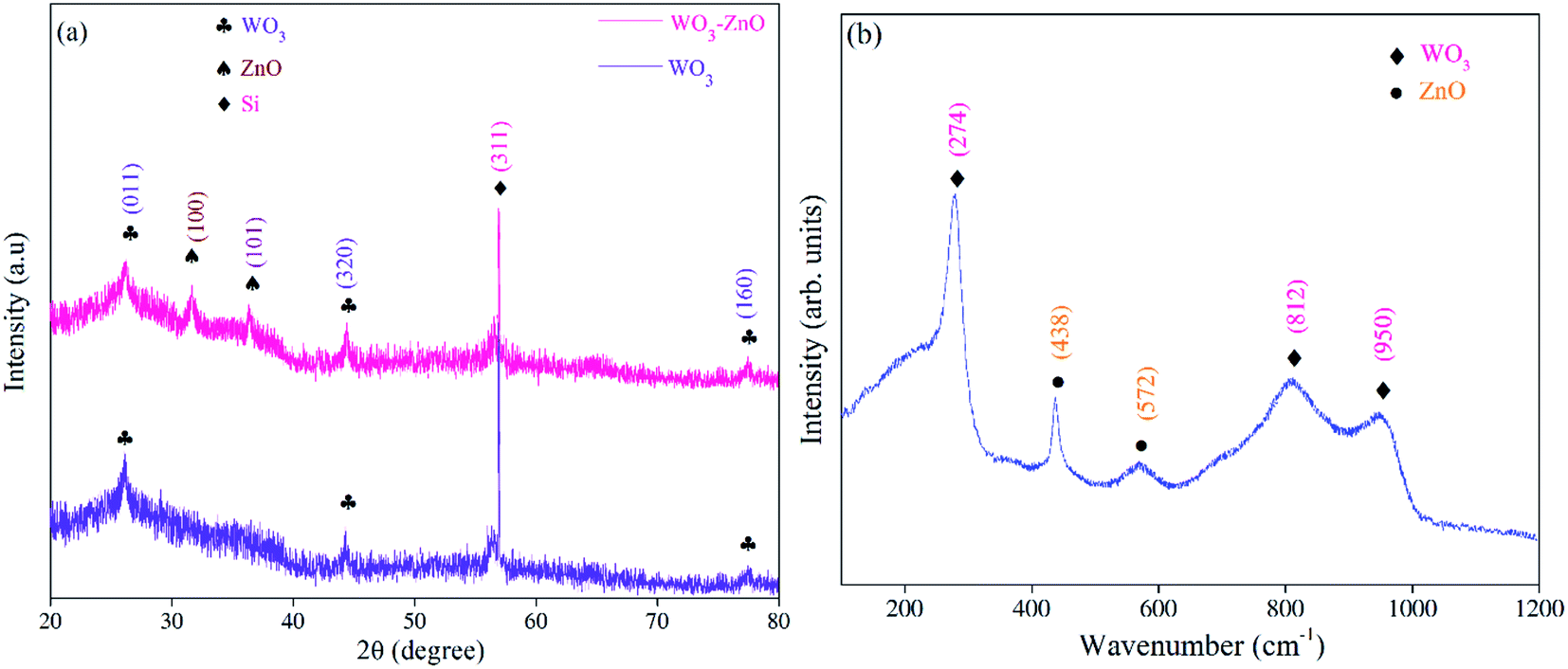
Fig. 1a depicts the XRD patterns of bare WO3 and Pd/WO3–ZnO composite thin films consists of monoclinic phase of WO3 corresponding to (011), (320) and (160) planes at 26.12°, 44.42° and 77.42° (JCPDS ICDD no. 00-005-0364). The Pd/WO3–ZnO composite thin film also consists of hexagonal phase of ZnO corresponding to (100) and (101) planes at 31.72° and 36.35° (JCPDS ICDD no. 00-003-0888). In addition, Fig. 1a shows the cubic phase of Si corresponding to (311) plane at 56.72° (JCPDS ICDD no. 00-002-0561). Here, no any XRD peak of Pd was detected due to small thickness (∼5 nm) of Pd in comparison to WO3–ZnO composite layer.
 |
| | Fig. 1 (a) XRD spectra of WO3 and Pd/WO3–ZnO thin films, and (b) Raman spectra of Pd/WO3–ZnO thin film. | |
A room temperature Raman spectra of as deposited Pd/WO3–ZnO composite layer was recorded to reveal more about the structural properties of the thin film. Fig. 1b depicts the Raman spectra of Pd/WO3–ZnO composite thin film from 100–1200 cm−1 to determine the phase of the sensing layer. The Raman spectrum of the sample demonstrates the vibrational peaks at 278, 438, 574, 812 and 950 cm−1. In this spectrum, the strongest band at 272 cm−1 assigned to the bending vibration modes of O–W5+–O indicate the existence of oxygen vacancies.38 The band observed at 812 cm−1 corresponds to the bridging stretching modes of O–W6+–O.39 Furthermore, the peak at 950 cm−1 can be attributed to the stretching modes of W6+![[double bond, length as m-dash]](https://www.rsc.org/images/entities/char_e001.gif) O terminal.38 On the other hand, the peak observed at 438 cm−1 was assigned as E2 band which belongs to wurtzite structure of zinc oxide. The E2 peak is often associated to the oxygen atoms only. The A1 (LO) mode at 574 cm−1 denotes the polar mode of vibrations of Zn and O atoms of ZnO which can be ascribed to the deficiency of oxygen vacancies in ZnO matrix.40 These result demonstrates that the structure of tungsten oxide and zinc oxide can be well indexed corresponding to a monoclinic and hexagonal phase respectively. Therefore, the observed Raman spectrum is well consistent with the XRD results.
O terminal.38 On the other hand, the peak observed at 438 cm−1 was assigned as E2 band which belongs to wurtzite structure of zinc oxide. The E2 peak is often associated to the oxygen atoms only. The A1 (LO) mode at 574 cm−1 denotes the polar mode of vibrations of Zn and O atoms of ZnO which can be ascribed to the deficiency of oxygen vacancies in ZnO matrix.40 These result demonstrates that the structure of tungsten oxide and zinc oxide can be well indexed corresponding to a monoclinic and hexagonal phase respectively. Therefore, the observed Raman spectrum is well consistent with the XRD results.
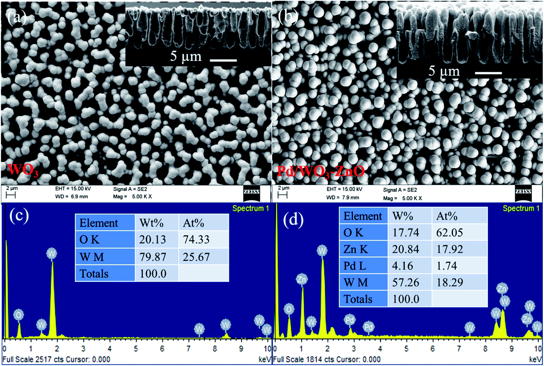
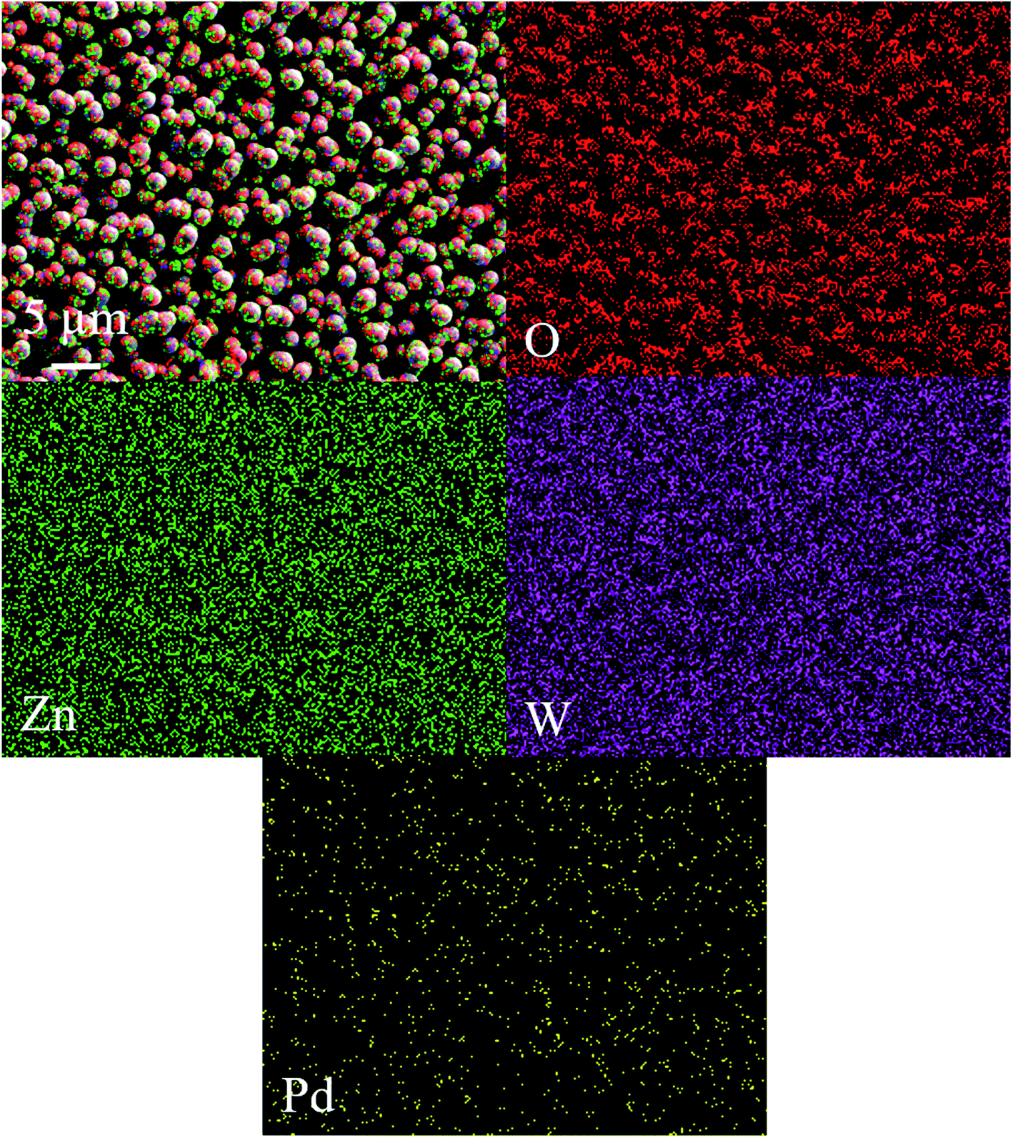
Fig. 2a and b depicts the FE-SEM images and corresponding cross-section view of as deposited bare WO3 and Pd/WO3–ZnO composite sensing layers. The porous silicon substrate (12 μm depth, 3 μm width) were filled with the bare WO3 composite layer of Pd/WO3–ZnO. The uniform and homogeneously distributed grain growth of WO3 and Pd/WO3–ZnO composite samples indicating the porous and dense packing microstructure with good monodispersity that collaborate to the low temperature fabrication of sensing thin films. The compositional study of bare WO3 and Pd/WO3–ZnO composite sensing film was examined using EDAX measurements, as shown in Fig. 2c and d. Only four elements, W, Zn, O and Pd are identified in this spectrum. The FE-SEM micrograph and EDS analyses of pure ZnO sample is shown in Fig. S1.† In addition, Fig. 3 depicts the mapping analysis of top view of Pd/WO3–ZnO composite sensing layer. Similarly, Fig. 4 shows the elemental mapping analysis of cross-sectional cut of Pd/WO3–ZnO composite sensing layer. These results reveal that all the elements are uniformly distributed inside the silicon pores. Therefore, it may be inferred that the Pd/WO3–ZnO composite sensor on porous silicon can absorb and desorb the H2 reversibly for a long time.
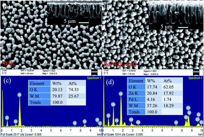 |
| | Fig. 2 (a and b) FE-SEM images with corresponding cross section images, and (c and d) EDS spectra of WO3 and Pd/WO3–ZnO thin films, respectively. | |
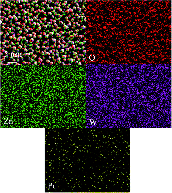 |
| | Fig. 3 Elemental mapping of surface images of Pd/WO3–ZnO thin film. | |
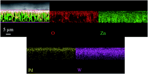 |
| | Fig. 4 Elemental mapping of cross sectional images of Pd/WO3–ZnO thin film. | |
3.2 Sensing performance
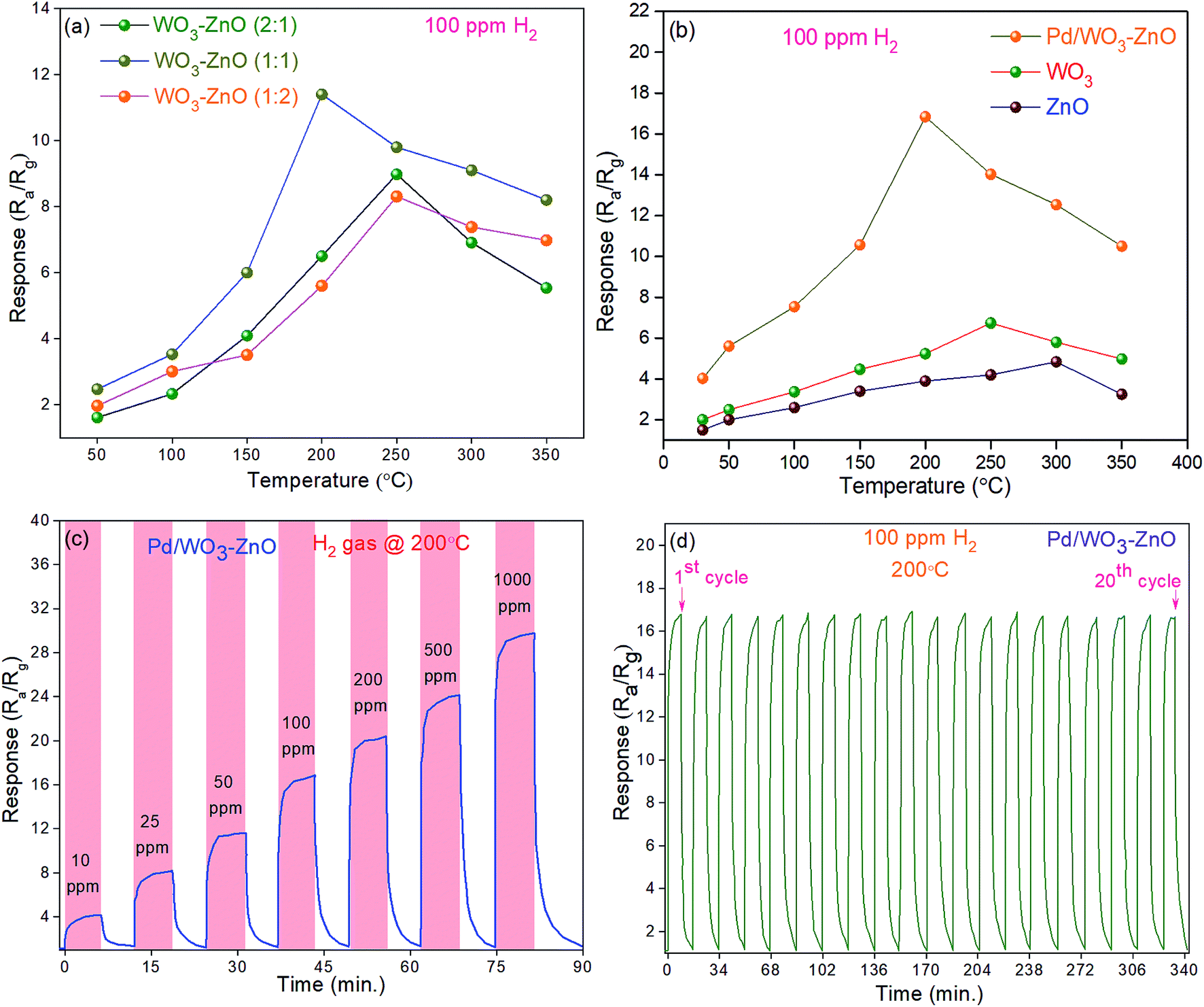
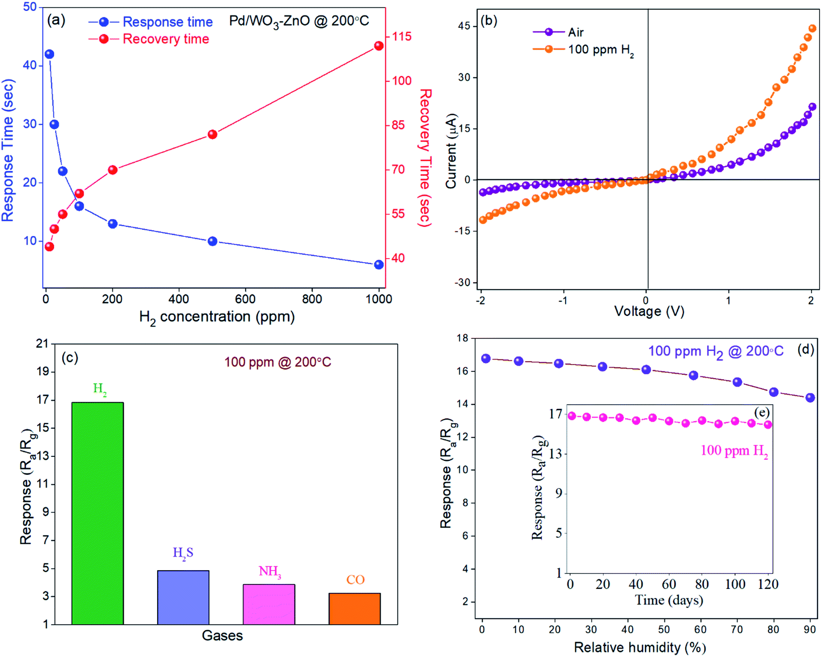
Fig. 5a depicts the gas response curve of WO3–ZnO (2:1), WO3–ZnO (1:1) and WO3–ZnO (1:2) thin film sensors as a function of operating temperature to 100 ppm H2 in dry air. Here, we observed that the WO3–ZnO (1:1) sensor exhibit the highest response due to same at% of W and Zn elements present in the sensing layer towards 100 ppm H2 at 200 °C. However, WO3–ZnO (2:1) and WO3–ZnO (1:2) thin film sensors exhibit the highest response at 250 °C. Due to formation of the heterojunction between two dissimilar materials the composite gas sensors will have better sensing performances than those of their individual components alone. It is customary that the sensor response will significantly depends on the elemental composition. In addition, the composite sensor exhibits the maximum response only when the catalytic action of the present components counterpart to each other.23 Therefore, WO3–ZnO (1:1) can show the best sensor response due to complement catalytic reaction of WO3 and ZnO would takes place at about equal elemental compositions. It might be due to more activation sites are available on WO3–ZnO (1:1) composite surface for oxygen adsorption at 200 °C. Thus, we have to choose WO3–ZnO (1:1) for further analysis through. Furthermore, we varied the Pd concentration from 0.97 at% to 2.95 at%. The result shows that the response increases with the Pd concentration up to 1.74 at%. Thereafter, response starts to decline as Pd concentration further increases to 2.95 at% [see Fig. S2(c)†]. It can be due to reduce the magnitude of activated sites on WO3–ZnO composite surface for oxygen adsorption as the number of attached Pd nanoparticles increases, and vice versa.41,42 Thereafter, the variation in the sensor response of bare ZnO, WO3 and Pd/WO3–ZnO (1:1) composite gas sensors was investigated at different operating temperatures to 100 ppm H2 in synthetic air (Fig. 5b). It can be observed that the gas sensors reveal the noticeable rise in the sensing response with rising the operating temperature. Meanwhile, the response turns to decline gradually if we further increase the temperature. Initially, it might be observed due to slow chemical activation between adsorbed analyte gas molecules and sensor surface at low temperatures.43 However, upon exposure to analyte gas the adsorbed gas molecules might be escape before reactions take place on the sensor surface at too high operating temperatures and hence the poor response as well.43 Based on these investigations, bare ZnO and WO3 sensors depict the maximum response at 300 °C and 250 °C, respectively, while for Pd/WO3–ZnO composite sensor the sensing response seems to be maximum at 200 °C (Fig. 5b). It indicates that the Pd/WO3–ZnO composite sensor depicts the high response to H2 as compare to bare ZnO and WO3 sensor through the whole temperature regime.44 This could be due to increase in the number of charge carriers in the depletion layer at the heterojunction, leading to remarkable enhance the response. Fig. 5c shows the sensing response characteristics of Pd/WO3–ZnO composite gas sensors upon exposure to the various concentration of H2 in synthetic air. These results reveals that the gas sensor might be able to detect the trace amount of hydrogen down to 10 ppm and exhibit a high response in the range of 10–1000 ppm at 200 °C. Fig. 5d depicts that Pd/WO3–ZnO composite sensor exhibit the stable response over 20 cycles towards 100 ppm of H2 at 200 °C. It indicates that the composite thin films exhibit the excellent repeatability to 100 H2 at 200 °C. The response and recovery time curves at various H2 concentrations were investigated in the range of 10–1000 ppm at 200 °C (Fig. 6a). For Pd/WO3–ZnO composite gas sensor, the fast response and recovery time was achieved to be 16 s and 62 s respectively towards 100 ppm H2 at 200 °C. The diffusion-limited kinetics at low hydrogen concentration can be attributed to achieve the high response time with reducing the target gas concentration.3 Fig. 6b depicts the I–V characteristics of the Pd/WO3–ZnO composite sensor, exhibits the rectifying diode behavior in absence/presence of hydrogen (100 ppm) at 200 °C. As shown in Fig. 6c, the selectivity of the sensors was also measured towards H2 gas with respect to other potentially hazardous gases such as carbon monoxide (CO), hydrogen sulfide (H2S) and ammonia (NH3) upon exposure to 100 ppm concentration at 200 °C. The Pd/WO3–ZnO composite sensor exhibited a remarkably high response (Ra/Rg = 16.8 ± 0.2) towards H2 and a weak response (Ra/Rg < 4.5 ± 0.3) with respect to other potentially interfering gases. This result shows that the Pd/WO3–ZnO sensor is highly selective towards H2 gas. The effect of moisture on the sensing response was examined under different humidity (0–90%) conditions towards 100 ppm H2 in synthetic air at 200 °C (Fig. 6d). This result indicate that about 15% decline in the response was observed for Pd/WO3–ZnO composite gas sensor. It can be explained as follow: when the active layer is exposed to a mixed gas, more water molecule get adsorbed on the sensor surface under high humidity conditions. Thereafter, the reaction between the water molecules and surface oxygen species deteriorated which contribute to fall in baseline resistance of the sensor and consequences in a decrease of its sensitivity.45 It can be due to the water vapors decline the sensor response by preventing the adsorption of target gas molecules on the sensor surface. Therefore, the change in sensor response and baseline resistance is mostly accredited to the high adsorption of water molecules on the top surface of the sensing layer in humid environment.46 Moreover, the response/recovery time versus relative humidity tests were also performed towards 100 ppm H2 gas in various humid conditions (dry air to 90% RH). At the same H2 concentration, results depict that the response and recovery time continuously rises with increasing RH (see Fig. S-3†). It may be due to the water molecules act as a barrier against the H2 adsorption and hence the migration of H2 molecules on the composite surface become rather difficult.47 Thus, the response and recovery of the proposed sensor to the mixed environment of H2 with dry air is rather faster than that of H2 with humidity. Furthermore, the stability test of the sensor was carried out at 100 ppm H2 concentration for four months (Fig. 6e). During the measurements, it indicate nearly constant response (∼5% change), demonstrating the remarkable long term stability of the composite sensor. The decrease in response may be due to heating the active sensing material after long time working at 200 °C temperature.48 Moreover, we have used porous silicon substrates to manipulate the structure of the oxide films and enhance the active surface area for the analyte gas molecules (high surface to volume ratio).32,33 Furthermore, the porous silicon may provide the reproducibility as well as long term stability towards H2 gas at 200 °C. Therefore, the Pd/WO3–ZnO composite thin film sensor is used for detecting the trace amount (10–1000 ppm) of H2 gas under harsh environment. The hydrogen sensing measurements were repeated four times and about 3% variation in the sensing properties was detected. Moreover, the proposed sensor can be established as a promising candidate for H2 sensing device application. The comparison of the WO3 and ZnO sensor systems for H2 gas is shown in Table S1.†
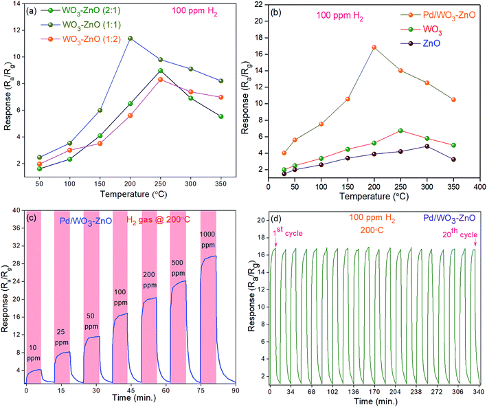 |
| | Fig. 5 (a) Gas response curve oFf WO3–ZnO (2:1), WO3–ZnO (1:1) and WO3–ZnO (1:2) thin film sensors as a function of operating temperature to 100 ppm H2 in dry air, (b) gas response curve of the bare ZnO, WO3 and Pd/WO3–ZnO (1:1) thin film sensor vs. operating temperatures to 100 ppm H2 gas in dry air, (c) gas response curve of Pd/WO3–ZnO thin film sensor as a function of the hydrogen concentration (10–1000 ppm) at 200 °C in dry air, (d) cyclic response curve of Pd/WO3–ZnO thin film sensor towards H2 with a gas concentration of 100 ppm at 200 °C in dry air. | |
 |
| | Fig. 6 (a) Response–recovery time curve of the Pd/WO3–ZnO (1:1) thin film sensor vs. H2 gas concentrations in dry air, (b) I–V curve of the Pd/WO3–ZnO (1:1) thin film sensor in 100 ppm H2 gas and dry air, (c) cross sensitivity curve of Pd/WO3–ZnO thin film sensor towards H2, CO, H2S and NH3 with a gas concentration of 100 ppm at 200 °C in dry air, (d) gas response curve of Pd/WO3–ZnO (1:1) thin film sensor as a function of the relative humidity in 100 ppm H2 at 200 °C, (e) stability curve of the Pd/WO3–ZnO (1:1) thin film sensor in 100 ppm H2 gas concentration in dry air at 200 °C. | |
3.3 Sensing mechanism
The basic reaction mechanism of n-type semiconductor sensors has been well documented using depletion layer or space charge model.49–51 Generally, the adsorption and desorption process of analyte gas molecules on the sensor surface played the prominent role in changing the resistance of sensor device. Therefore, the basic working principle of bare WO3 layer towards H2 involves the following steps: firstly, the oxygen molecules present in air environment can adsorbed on the top surface of WO3 and extract the electron from the conduction band of WO3, leading to reduce the electron concentration and hence the initial resistance increases.52 Secondly, when these chemisorbed oxygen species react with the H2 molecules, releasing the electron back to the conduction band of WO3, thereby increasing the electron conductivity caused to declines in resistance of sensing thin film.| | |
O2(gas) → 2O(adsorbed)
| (1) |
| | |
O(adsorbed) + e(from WO3)− → O−
| (2) |
| | |
H2 + O− → H2O + e(to WO3)−
| (3) |
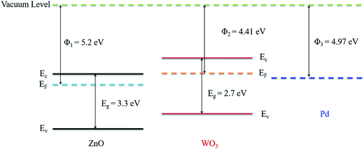
But the sensor working mechanism of WO3–ZnO composite becomes rather different from the bare WO3 or ZnO oxide layer. In WO3–ZnO composite layer, heterojunctions are created at the grain boundaries between WO3 and ZnO which can significantly contribute to the reducing gas effect in oxide composite materials. It might be due to the formation of n–n heterojunction between two dissimilar materials n-ZnO and n-WO3 having different work function of 4.41 eV and 5.2 eV respectively.53,54 The value of energy band gap for ZnO and WO3 are about 3.3 eV and 2.7 eV, respectively.55 When two dissimilar materials WO3 and ZnO formed an electrical connection at the interface, then the electrons will start to flow from high energy conduction band to the lower energy conduction band (from WO3 to ZnO) until the Fermi levels have equilibrated. Due to lower work function of WO3, a depletion region is created towards WO3 at the n–n heterostructures interface whereas an accumulation region is formed towards ZnO caused by transfer the electrons from WO3 to ZnO. This results in bending the energy band at the WO3/ZnO heterojunction which leads to higher resistance state of the sensing material than bare WO3.56 In ambient air, the oxygen species adsorbed at the grain boundaries of WO3 and ZnO and shield the WO3/ZnO heterojunctions such that the conducting electrons being trapped, and the composite layer become more resistive.55,57 This results to create the barrier height at the WO3/ZnO heterojunction. Thereafter, the exposed H2 gas molecules will reduce the adsorbed oxygen species on the surface. It can be suggested that due to surface reaction the electrons will be generated and flow along the WO3/ZnO interfaces, resulting in shrinkage of the electron-depletion layer and barrier height between ZnO and WO3. This result to decreases the overall sensor resistance, when a reducing gas is supplied.
Furthermore, when Pd nanoparticles were decorated on the WO3–ZnO (1:1) sensor surface, the electron starts to flow from WO3 to Pd nanoparticles, which leads to expand the depletion layer towards WO3. As we know the work function of Pd is 4.97 eV. This will further enhance the device resistance of WO3–ZnO (1:1) composite sensor. Moreover, the thin layer of Pd nanoparticles on the WO3–ZnO (1:1) sensor surface can easily dissociate the H2 molecules into Hads+ ions via catalytic reaction.58 Thereafter, a bend bending occurs due to difference in Fermi levels of the materials, leads to a formation of potential energy barrier at the interface.59 This process can facilitates the significant adsorption of oxygen species on the Pd/WO3–ZnO sensor surface thereby improving the charge transfer dynamics between the analyte gas molecules and the sensor surface. This enhances the initial device resistance of the Pd/WO3–ZnO composite sensor. Fig. 7 show the energy band diagram of the mechanism involved at the Pd/WO3–ZnO heterojunctions. In addition, the banding diagram of the Pd/WO3–ZnO sensor which establish the bending of the band after the equalization of the Fermi level is illustrated in Fig. 8. Therefore, it is suggested that the conduction band near the boundaries will bend upward, increasing the energy difference between the Fermi level and conduction band.
 |
| | Fig. 7 Energy band diagram of Pd/WO3–ZnO thin film sensor before thermal equilibrium. | |
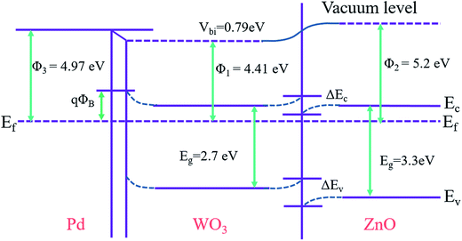 |
| | Fig. 8 The energy banding diagram of the Pd/WO3–ZnO sensor which establish the bending of the band after the equalization of the Fermi levels. | |
Owing to the contribution of n–n heterojunction, the enhancement in the sensing response of Pd/WO3–ZnO composite towards H2 gas is noteworthy. The main contributing mechanisms involved at n–n junction is following: the adsorbed oxygen ions react with the exposed reducing H2 gas molecules on the Pd/WO3–ZnO hetero-junction sensor surface and releasing the electron back to the Pd/WO3–ZnO composite layer. This result to decreases the overall sensor resistance, when a reducing gas is supplied. Furthermore, during the recovery process, in absence of H2 gas the electron concentration on the junction declines, caused to recover the original resistance of the sensor.
4. Conclusion
In summary, we have synthesized a bare ZnO, WO3 and Pd/WO3–ZnO composite heterostructures on porous silicon substrates using reactive DC sputtering technique and their sensing properties towards H2 was investigated in detail. At low temperature, the excellent hydrogen sensing behavior of Pd/WO3–ZnO composite sensor is attributed to the formation of n–n heterojunction at the interface. Here, the formation of depletion layer at the n–n heterojunction significantly enhances the sensor response in comparison with a bare ZnO and WO3 sensors. Such gas sensor can exhibit high response (Ra/Rg ∼16.8) with fast response time (16 s) and good selectivity to 100 ppm H2 at 200 °C. This study has also demonstrated the highly stable (120 days) and reproducible (20th cycles) sensor response towards 100 ppm H2 at low temperature of 200 °C. Therefore, the porous silicon sensor systems clearly demonstrate a new approach to design and fabricate the low temperature chemiresistive gas sensors with remarkable performance.
Conflicts of interest
The authors declare no competing financial interests.
Acknowledgements
The author A. K. would like to acknowledge the financial support from the University Grant Commission, India (Grant code: 7412-30-044).
References
- C. E. Gregoire-Padró, Energy Fuels, 1998, 12, 1–2 CrossRef.
- S. Yi, S. Tian, D. Zeng, K. Xu, X. Peng, H. Wang, S. Zhang and C. Xie, Sens. Actuators, B, 2014, 204, 351–359 CrossRef CAS.
- S.-J. Choi, S. Chattopadhyay, J. J. Kim, S.-J. Kim, H. L. Tuller, G. C. Rutledge and I.-D. Kim, Nanoscale, 2016, 8, 9159–9166 RSC.
- L. Schlapbach and A. Zuttel, Nature, 2001, 414, 353–358 CrossRef CAS PubMed.
- A. S. Arico, P. Bruce, B. Scrosati, J.-M. Tarascon and W. van Schalkwijk, Nat. Mater., 2005, 4, 366–377 CrossRef CAS PubMed.
- L.-F. Wang, J.-Z. Qiu, J.-L. Liu, Y.-C. Chen, J.-H. Jia, J. Jover, E. Ruiz and M.-L. Tong, Chem. Commun., 2015, 51, 15358–15361 RSC.
- Z. Zhang, X. Zou, L. Xu, L. Liao, W. Liu, J. Ho, X. Xiao, C. Jiang and J. Li, Nanoscale, 2015, 7, 10078–10084 RSC.
- B. Sakintuna, F. Lamari-Darkrim and M. Hirscher, Int. J. Hydrogen Energy, 2007, 32, 1121–1140 CrossRef CAS.
- D. Jung, M. Han and G. S. Lee, Sens. Actuators, B, 2014, 204, 596–601 CrossRef CAS.
- A. Sanger, P. K. Jain, Y. K. Mishra and R. Chandra, Sens. Actuators, B, 2017, 242, 694–699 CrossRef CAS.
- M. Law, H. Kind, B. Messer, F. Kim and P. Yang, Angew. Chem., 2002, 114, 2511–2514 CrossRef.
- Q. Kuang, C. Lao, Z. L. Wang, Z. Xie and L. Zheng, J. Am. Chem. Soc., 2007, 129, 6070–6071 CrossRef CAS PubMed.
- S.-W. Choi, A. Katoch, J.-H. Kim and S. S. Kim, J. Mater. Chem. C, 2015, 3, 1521–1527 RSC.
- S. Jain, A. Sanger, S. Chauhan and R. Chandra, Mater. Res. Express, 2014, 1, 035046 CrossRef.
- W. M. Tang, P. T. Lai, J. P. Xu and C. L. Chan, Sens. Actuators, A, 2005, 119, 63–67 CrossRef CAS.
- Y.-H. Choi and S.-H. Hong, Sens. Actuators, B, 2007, 125, 504–509 CrossRef CAS.
- Z. H. Lim, Z. X. Chia, M. Kevin, A. S. W. Wong and G. W. Ho, Sens. Actuators, B, 2010, 151, 121–126 CrossRef CAS.
- C. Wongchoosuk, A. Wisitsoraat, D. Phokharatkul, A. Tuantranont and T. Kerdcharoen, Sensors, 2010, 10, 7705 CrossRef CAS PubMed.
- Z. Wang, Z. Li, J. Sun, H. Zhang, W. Wang, W. Zheng and C. Wang, J. Phys. Chem. C, 2010, 114, 6100–6105 CAS.
- A. Katoch, J.-H. Kim, Y. J. Kwon, H. W. Kim and S. S. Kim, ACS Appl. Mater. Interfaces, 2015, 7, 11351–11358 CAS.
- M. Horprathum, T. Srichaiyaperk, B. Samransuksamer, A. Wisitsoraat, P. Eiamchai, S. Limwichean, C. Chananonnawathorn, K. Aiempanakit, N. Nuntawong, V. Patthanasettakul, C. Oros, S. Porntheeraphat, P. Songsiriritthigul, H. Nakajima, A. Tuantranont and P. Chindaudom, ACS Appl. Mater. Interfaces, 2014, 6, 22051–22060 CAS.
- A. Kumar, A. Sanger, A. Kumar and R. Chandra, RSC Adv., 2016, 6, 47178–47184 RSC.
- C. Wang, L. Yin, L. Zhang, D. Xiang and R. Gao, Sensors, 2010, 10, 2088 CrossRef CAS PubMed.
- Q. Xu, D. Ju, Z. Zhang, S. Yuan, J. Zhang, H. Xu and B. Cao, Sens. Actuators, B, 2016, 225, 16–23 CrossRef CAS.
- T. Wagner, S. Haffer, C. Weinberger, D. Klaus and M. Tiemann, Chem. Soc. Rev., 2013, 42, 4036–4053 RSC.
- D. J. Wales, J. Grand, V. P. Ting, R. D. Burke, K. J. Edler, C. R. Bowen, S. Mintova and A. D. Burrows, Chem. Soc. Rev., 2015, 44, 4290–4321 RSC.
- J. Zhang, X. Liu, G. Neri and N. Pinna, Adv. Mater., 2016, 28, 795–831 CrossRef CAS PubMed.
- A. Sanger, A. Kumar, S. Chauhan, Y. K. Gautam and R. Chandra, Sens. Actuators, B, 2015, 213, 252–260 CrossRef CAS.
- K. Seong-Jeen, P. Jae-Yoon, L. Sang-Hoon and Y. Seung-Hwan, J. Phys. D: Appl. Phys., 2000, 33, 1781 CrossRef.
- J. Das, S. M. Hossain, S. Chakraborty and H. Saha, Sens. Actuators, A, 2001, 94, 44–52 CrossRef CAS.
- T. Karacali, U. C. Hasar, I. Y. Ozbek, E. A. Oral and H. Efeoglu, J. Lightwave Technol., 2013, 31, 295–305 CrossRef CAS.
- S. E. Lewis, J. R. DeBoer, J. L. Gole and P. J. Hesketh, Sens. Actuators, B, 2005, 110, 54–65 CrossRef CAS.
- I. Schechter, M. Ben-Chorin and A. Kux, Anal. Chem., 1995, 67, 3727–3732 CrossRef CAS.
- K. Luongo, A. Sine and S. Bhansali, Sens. Actuators, B, 2005, 111, 125–129 CrossRef.
- A. Sanger, A. Kumar, A. Kumar, P. K. Jain, Y. K. Mishra and R. Chandra, Ind. Eng. Chem. Res., 2016, 55, 9452–9458 CrossRef CAS.
- A. Sanger, A. Kumar, A. Kumar and R. Chandra, Sens. Actuators, B, 2016, 234, 8–14 CrossRef CAS.
- A. Kumar, A. Sanger, A. Kumar and R. Chandra, RSC Adv., 2016, 6, 77636–77643 RSC.
- M. Li, M. Hu, D. Jia, S. Ma and W. Yan, Sens. Actuators, B, 2013, 186, 140–147 CrossRef CAS.
- F. Guojia, L. Zuli and K. L. Yao, J. Phys. D: Appl. Phys., 2001, 34, 2260 CrossRef.
- Z. Zulkifli, M. Subramanian, T. Tsuchiya, M. S. Rosmi, P. Ghosh, G. Kalita and M. Tanemura, RSC Adv., 2014, 4, 64763–64770 RSC.
- C.-M. Chang, M.-H. Hon and I.-C. Leu, ACS Appl. Mater. Interfaces, 2013, 5, 135–143 CAS.
- T.-R. Rashid, D.-T. Phan and G.-S. Chung, Sens. Actuators, B, 2013, 185, 777–784 CrossRef CAS.
- L. Liu, S. Li, J. Zhuang, L. Wang, J. Zhang, H. Li, Z. Liu, Y. Han, X. Jiang and P. Zhang, Sens. Actuators, B, 2011, 155, 782–788 CrossRef CAS.
- X. Liu, J. Zhang, X. Guo, S. Wang and S. Wu, RSC Adv., 2012, 2, 1650–1655 RSC.
- J. Gong, Q. Chen, M.-R. Lian, N.-C. Liu, R. G. Stevenson and F. Adami, Sens. Actuators, B, 2006, 114, 32–39 CrossRef CAS.
- A. Sanger, A. Kumar, A. Kumar, J. Jaiswal and R. Chandra, Sens. Actuators, B, 2016, 236, 16–26 CrossRef CAS.
- Q. Qi, T. Zhang, X. Zheng, H. Fan, L. Liu, R. Wang and Y. Zeng, Sens. Actuators, B, 2008, 134, 36–42 CrossRef CAS.
- J. Guo, J. Zhang, M. Zhu, D. Ju, H. Xu and B. Cao, Sens. Actuators, B, 2014, 199, 339–345 CrossRef CAS.
- D. Ju, H. Xu, J. Zhang, J. Guo and B. Cao, Sens. Actuators, B, 2014, 201, 444–451 CrossRef CAS.
- Z. Li, Q. Zhao, W. Fan and J. Zhan, Nanoscale, 2011, 3, 1646–1652 RSC.
- X. Li, X. Zhou, H. Guo, C. Wang, J. Liu, P. Sun, F. Liu and G. Lu, ACS Appl. Mater. Interfaces, 2014, 6, 18661–18667 CAS.
- K. Suematsu, N. Ma, M. Yuasa, T. Kida and K. Shimanoe, RSC Adv., 2015, 5, 86347–86354 RSC.
- D.-X. Ju, H.-Y. Xu, Z.-W. Qiu, Z.-C. Zhang, Q. Xu, J. Zhang, J.-Q. Wang and B.-Q. Cao, ACS Appl. Mater. Interfaces, 2015, 7, 19163–19171 CAS.
- H. Li, W. Xie, T. Ye, B. Liu, S. Xiao, C. Wang, Y. Wang, Q. Li and T. Wang, ACS Appl. Mater. Interfaces, 2015, 7, 24887–24894 CAS.
- C. Feng, X. Li, J. Ma, Y. Sun, C. Wang, P. Sun, J. Zheng and G. Lu, Sens. Actuators, B, 2015, 209, 622–629 CrossRef CAS.
- N. Dac Dien, D. Duc Tho, V. Xuan Hien, D. Duc Vuong and N. Duc Chien, Adv. Nat. Sci.: Nanosci. Nanotechnol., 2016, 7, 015004 CrossRef.
- Y. Liu, J. Yu and P. T. Lai, Int. J. Hydrogen Energy, 2014, 39, 10313–10319 CrossRef CAS.
- A. S. M. I. Uddin, U. Yaqoob and G.-S. Chung, Sens. Actuators, B, 2016, 226, 90–95 CrossRef CAS.
- W. Tang, J. Wang, P. Yao and X. Li, Sens. Actuators, B, 2014, 192, 543–549 CrossRef CAS.
Footnote |
| † Electronic supplementary information (ESI) available. See DOI: 10.1039/c7ra05341j |
|
| This journal is © The Royal Society of Chemistry 2017 |
Click here to see how this site uses Cookies. View our privacy policy here. 
 Open Access Article
 This Open Access Article is licensed under a
  ,
Ashwani Kumar
,
Ashwani Kumar