DOI:
10.1039/C7RA05429G
(Paper)
RSC Adv., 2017,
7, 39657-39665
Multi-band visible photoresponse study of Co2+ doped ZnO nanoparticles
Received
13th May 2017
, Accepted 5th August 2017
First published on 14th August 2017
Abstract
In this article, near UV (NUV) and near UV-visible photodetectors (PDs) were fabricated using pure (ZnO) and Co doped ZnO (Zn1−xCoxO) nanoparticles synthesised by co-precipitation method. The structural, morphological, compositional and chemical state analysis of the nanoparticles were done using X-ray diffractometry, transmission electron microscopy, energy dispersive spectrometry and X-ray photoelectron spectrometry respectively. The optical spectra which were recorded using a UV-Vis spectrometer exhibited the presence of absorption peaks in the visible region for Co doped ZnO due to d–d transitions. Enhanced photoresponse in the NUV region was found in lower doping concentrations and all the Co doped ZnO photodetectors showed a noticeable response to visible light sources. A maximum responsivity of 63 mA W−1 and quantum efficiency of ∼20% was achieved in the NUV region for the PD fabricated with 2 at% Co doping. The 2 at% Co doped ZnO based photodetector showed efficiency in the range 11–35% for the wavelengths from 401 to 634 nm.
1. Introduction
Semiconductor based photodetectors (PDs) have caught much research attention for the past few decades. In recent years much effort has been devoted to ZnO owing to its remarkable and unique opto-electronic properties, non-toxicity, high thermal and chemical stability, ability for use in harsh environments, radiation hardness, eco friendliness, low cost, availability etc. ZnO is an intrinsically n-type semiconductor having a hexagonal wurtzite structure with a large direct band gap of ∼3.37 eV. It exhibits a large excitonic binding energy of ∼60 meV at room temperature.1–4 The wide band gap limits its light absorption at the near ultra-violet (NUV) region, hence ZnO is most preferred for UV light detection and many works have reported on the fabrication of ZnO based UV PDs.5–8 Through the suitable addition of impurities through doping or alloying, the properties of ZnO can be effectively controlled and also the absorbing spectral region can be shifted or extended.9–11 Many research groups have reported the fabrication of ZnO based PDs in the deep UV region by increasing the bandgap with Mg doping.12–14 Recently, Shewale et al. reported the fabrication of Mg doped ZnO nanorod array film based PDs by pulsed laser deposition (PLD) at different growth times and achieved a maximum responsivity of 22.33 mA W−1.15
Considering the wide range of applications like flame detection, environmental monitoring and image sensing, visible light detection is also much necessary and the works on ZnO based visible detectors are very few.16 With Cd doping, the bandgap of ZnO can be red shifted to extend the absorption towards blue region; still further shifting is again limited.17,18 In our previous work, with Cd alloying the ZnO thin film band gap was shifted to 2.66 eV and the fabricated PDs exhibited enhanced photoresponse in NUV and blue regime.19 Studies on the optical properties of Co doped ZnO reports the presence of absorption peaks in the visible region due to 3d ligand field split states.20–22 This can be utilized for the fabrication of visible light detectors without losing the other advantages of ZnO. Also, doping with transition metals like Co hinders the recombination of electron hole pair generated from optical absorption which also improves the optical properties of ZnO.23 The ionic and covalent radius of Co (0.072 nm and 0.116 nm) matches with that of Zn (0.074 nm and 0.125 nm), so it can be properly alloyed to the lattice without disturbing the crystal structure of ZnO and not much changing the lattice strain. Johnson et al. studied the temperature dependant visible light photoconductivity of ZnO films with varying Co doping concentration and obtained maximum light conversion efficiency at lower concentration, which is much smaller than the achievable solubility limit of Co2+ ions in ZnO lattice.24 So far, no works have been reported on the fabrication of Co alloyed ZnO visible light detectors. The present work aims at analysing the material properties of pure and Co alloyed ZnO, and attempts for the first time to fabricate PDs for detection in NUV as well visible regime.
2. Materials and methods
ZnO nanoparticles were synthesised by co-precipitation method using zinc acetate di-hydrate (Zn(CH3COO)2·2H2O), cobalt chloride (CoCl2) and sodium hydroxide (NaOH) as precursors. 0.2 M zinc acetate di-hydrate and cobalt chloride corresponding to Co/Zn atomic percentage of 0, 1, 2, 3, and 4 were dissolved in 100 ml deionized (DI) water for the synthesis of Zn1−xCoxO for x = 1, 2, 3 and 4 respectively. 0.4 M NaOH prepared in 100 ml DI water was added to it drop wise and the resultant solution with precipitate was stirred for 4 h again. The precipitate was washed many times in DI water and ethanol followed by filtering and drying at 150 °C for 1 h. The Zn1−xCoxO nanoparticles thus obtained were annealed in muffle furnace at 500 °C for 2 h.
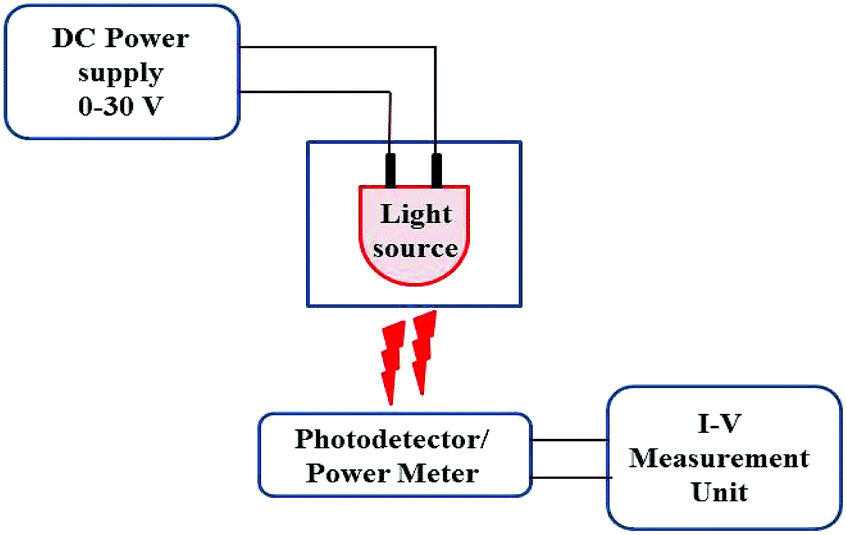
The material properties of synthesised nanoparticles were investigated using X-ray diffractometer (XRD), transmission electron microscope (TEM), energy dispersive spectrometer (EDS), X-ray photoelectron spectrometer (XPS) and UV-Vis spectrometer in Diffuse Reflectance Spectroscopy (DRS) mode. For the fabrication of PDs 10 mm circular pellets of these nanoparticles were made using pelletizer at an applied pressure of 80 kg cm−2 followed by annealing at 500 °C for 2 h to densify the pellet, interdigitated electrodes were made over the pellet using silver paste. Photo-response behaviour of PDs towards different wavelength lights were studied using Agilent B2901A Precision I–V (current–voltage) measurement unit with UV and visible LEDs as light source. The measuring procedure and details of the source LED parameters were explained in our previous work.19 The wavelength and power values of LED sources are given in Fig. 1 and Table 1, respectively. The combined schematic for power measurement of LEDs and photoresponse studies of fabricated PDs is shown in Fig. 2.
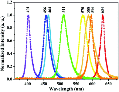 |
| | Fig. 1 Emission spectra of LED light sources. | |
Table 1 Output power of LED sources at different forward voltages
| Forward voltage, V (volts) and output power, P (mW) for different LED sources |
| 401 nm |
456 nm |
465 nm |
511 nm |
570 nm |
588 nm |
596 nm |
634 nm |
| V |
P |
V |
P |
V |
P |
V |
P |
V |
P |
V |
P |
V |
P |
V |
P |
| 3.2 |
3.46 |
2.8 |
1.038 |
2.6 |
0.12 |
3.2 |
1.33 |
2.2 |
1.88 |
2 |
0.395 |
2.2 |
0.777 |
1.8 |
0.2 |
| 3.4 |
11.02 |
3 |
6.18 |
2.8 |
1.2 |
3.4 |
2.33 |
2.4 |
6.155 |
2.2 |
1.086 |
2.3 |
1.271 |
1.9 |
0.84 |
| 3.6 |
14.09 |
3.2 |
10.77 |
3 |
3.088 |
3.6 |
3.33 |
2.6 |
9.008 |
2.4 |
2.38 |
2.4 |
3.775 |
2 |
1.68 |
| 3.8 |
19.35 |
3.4 |
19.6 |
3.2 |
6.612 |
3.8 |
4.33 |
2.8 |
10.16 |
2.6 |
4.29 |
2.5 |
10.02 |
2.1 |
6.72 |
| 4 |
23.66 |
3.6 |
27.23 |
3.4 |
10.92 |
4 |
5.33 |
3 |
12.06 |
|
|
|
|
|
|
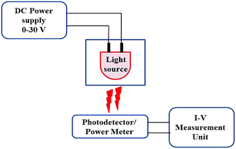 |
| | Fig. 2 Schematic of LED power measurement and photodetection studies of PDs. | |
3. Results and discussions
3.1. Characterization of ZnxCo1−xO nanoparticles
ZnO nanoparticles alloyed with Co (Zn1−xCoxO) at 1, 2, 3 and 4 atomic percentages (Zn0.99Co0.01O, Zn0.98Co0.02O, Zn0.97Co0.03O and Zn0.96Co0.04O) are represented as ZC1, ZC2, ZC3 and ZC4 respectively.
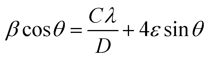
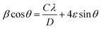
The XRD pattern shown in Fig. 3 confirms the formation of Zn1−xCoxO nanoparticles with hexagonal wurtzite structure. No additional peaks have been observed in Co alloyed nanoparticles indicating the absence of secondary phase formation like CoO or Co-metal/metal clusters. Also, the crystallinity of ZnO has not changed much after Co addition which can be attributed to the substitution of similar ionic radii Co2+ in Zn2+ site. The observance of sharp peaks indicates the high crystalline nature of synthesized nanopowders. The average crystallite size (D) of nanoparticles were estimated using Williamson and Hall (W–H) plot (Fig. 4) from the Cauchy–Lorentzian relation.25
| |
 | (1) |
where,
C is the shape factor,
θ is the diffraction angle and
λ is the X-ray wavelength. The change in crystallite size with alloy composition is shown in
Fig. 4. An increase in crystallite size was observed with increase in concentration of Co (
Fig. 5), which is similar to the previously reported studies.
26 However as the doping concentration increased up to 4 at% a reduction in size was seen, which may be due to the hindrance in grain growth or grain splitting effect with more Co concentration.
27
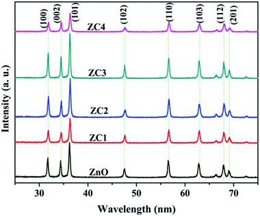 |
| | Fig. 3 XRD pattern of Zn1−xCoxO nanopowders. | |
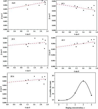 |
| | Fig. 4 W–H plots and crystallite size of Zn1−xCoxO nanopowders at different doping concentrations. | |
 |
| | Fig. 5 TEM and EDS data of Zn1−xCoxO nanopowders. | |
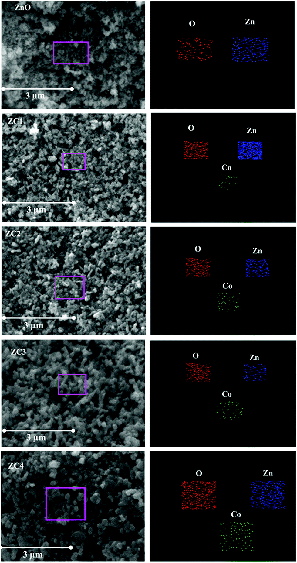
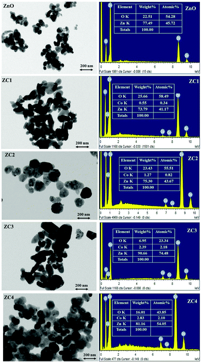
The morphology of the nanoparticles obtained using TEM imaging and the elemental composition determined using EDS analysis is shown in Fig. 5. Homogeneously distributed disc shaped nanoparticles with an average diameter in the range of 40–50 nm was observed from TEM analysis. All the compositions, the morphology of the system is found to be same and also the size distributions between the nanodiscs of different compositions are found to be in narrow range which will not remarkably affect the system efficiency. EDS analysis confirmed the presence of Zn, Co and O in the synthesized nanopowders. The atomic percentage obtained from EDS is shown in the inset of Fig. 5. Elemental mapping was performed to view the relative elemental distribution in nanoparticles and is revealed in Fig. 6. It shows that the elements Zn, O and CO are homogeneously distributed and also clearly depicts the increase in concentration of Co atoms in the nanoparticle upon increasing the doping concentration.
 |
| | Fig. 6 Elemental mapping of Zn1−xCoxO nanopowders. | |
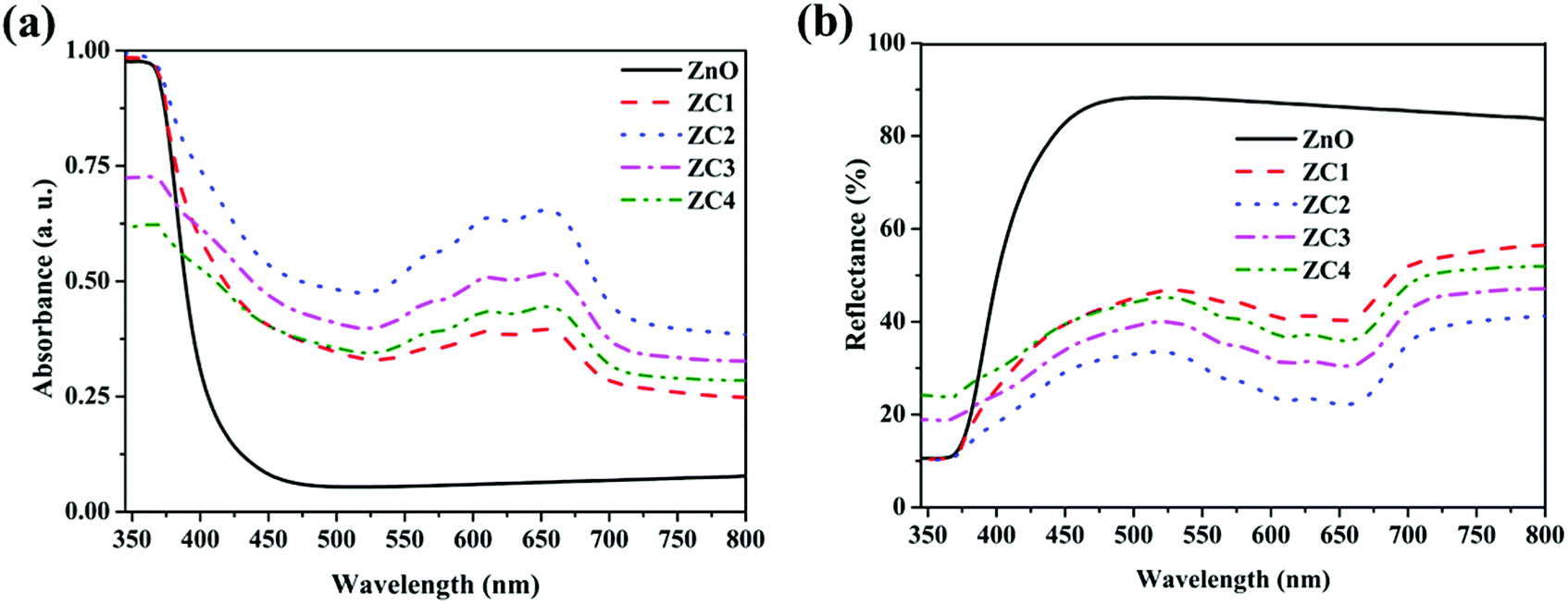
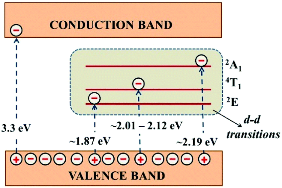
Fig. 7a and b shows the optical absorbance and reflectance spectra of Zn1−xCoxO nanoparticles recorded in DRS mode, respectively. With Co doping, the three characteristic absorption peaks corresponds to the d–d transition of Co2+ ions in tetrahedral co-ordination has been observed (563 nm, 610 nm and 657 nm) in the visible region.28 This confirms that most of the Co2+ occupies the Zn2+ sites in ZnO lattice, rather than precipitating as cobalt oxide (CoO) or Co metal.29 The series of absorption is due to the crystal field transitions from 2A1, 4T1 and 2E multiplets.20 Fig. 8 shows the schematic of absorption levels of Co2+ ions in ZnO lattice. The intensity of these peaks and UV absorption peak is found to be increased with Co doping up to 2% and then decreases due to the increased Co content.24 The decreased absorption in ZC3 might also have resulted from the increased agglomeration as seen from the TEM images which reduces the surface area for absorption.30 For 4% doping, the decreased crystallinity indicated by the reduced XRD peak intensity of ZC4 may also be a reason behind the decrease in absorbance.24
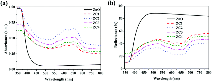 |
| | Fig. 7 (a) Absorbance and (b) reflectance spectra of Zn1−xCoxO nanopowders. | |
 |
| | Fig. 8 Schematic of Co2+ absorption levels in ZnO lattice. | |
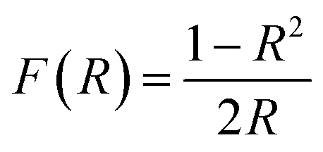
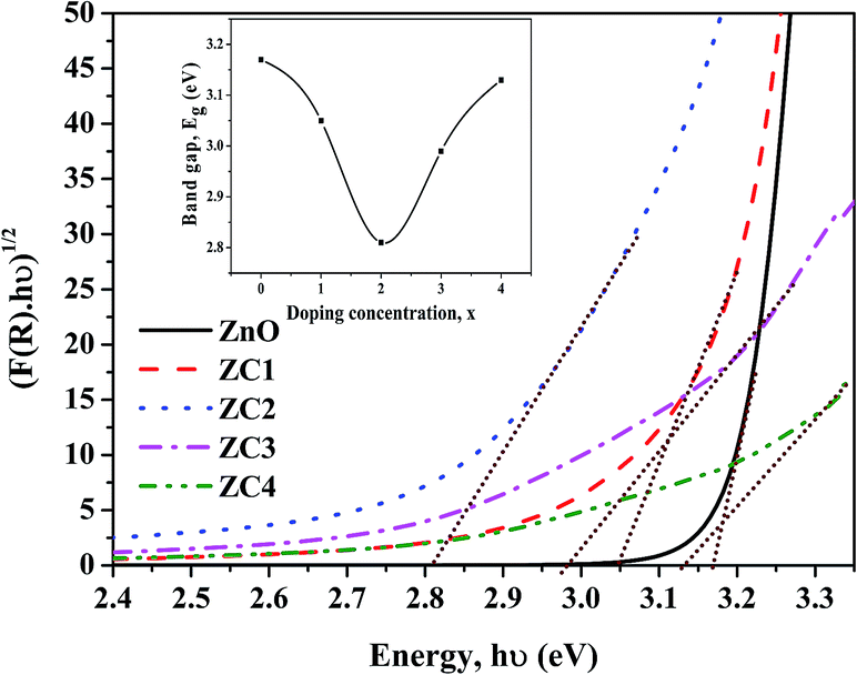
From the DRS data the bandgap of Zn1−xCoxO nanopowders was estimated using Kubelka Monk relation,31
| |
 | (2) |
where,
F(
R) is the Kubelka Munk function and
R is the reflectance. The inset of Kubelka Monk plot (
Fig. 9) shows the bandgap variation with doping concentration. It can be seen that the bandgap of ZnO has decreased with the incorporation of Co
2+ ions, which can be attributed to the decrease of spin-up band.
32 Further, the red shift is seen to be less at higher concentration, which can be due to the influence of Burstein–Moss effect.
27
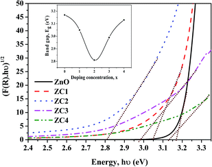 |
| | Fig. 9 Kubelka monk plot for Zn1−xCoxO nanopowders (inset: bandgap variation of Zn1−xCoxO nanopowders with doping concentration). | |
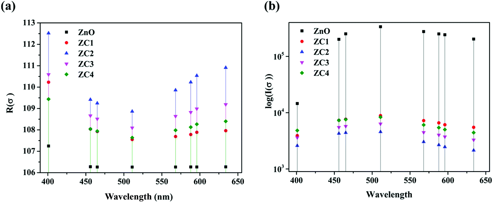
From the DRS data the optical conductivity (σ) of the Zn1−xCoxO nanopowders at each source wavelengths were estimated using the relations.33
where,
ω = (2
c/
λ) is the angular frequency,
c is the velocity of light,
ε is the permittivity and
ε0 is the permittivity of free space.
Fig. 10 shows that the improvement in the optical conductivity of ZnO, at smaller concentrations of Co doping which is in line with the previous reports.
24,34 Johnson
et al. reported that this increase in photoconductivity with Co incorporation can be further enhanced at higher temperatures by a thermally assisted ionization process. Since our work focus on room temperature photodetection, variable temperature studies have not been performed.
35
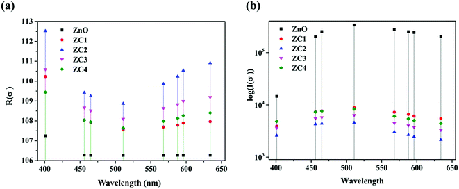 |
| | Fig. 10 (a) Real and (b) log or imaginary part of conductivity of Zn1−xCoxO nanopowders. | |
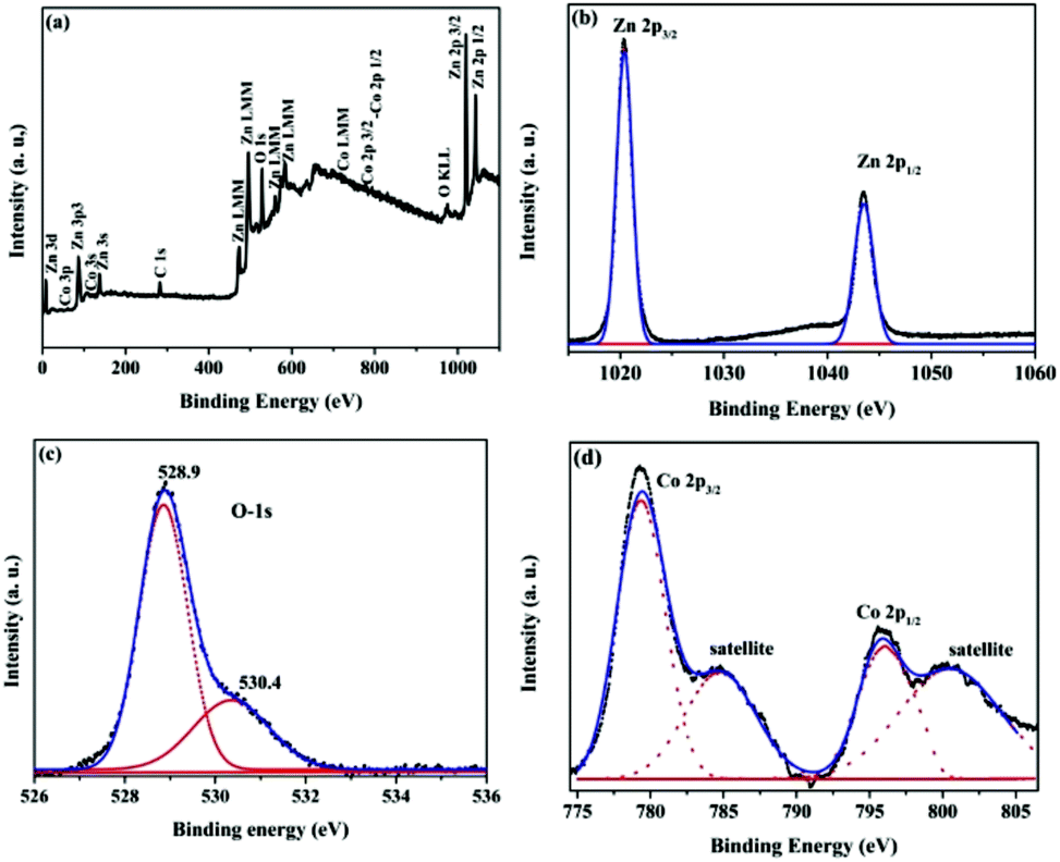
Further, to confirm the presence of elements and to examine its chemical states in the obtained nanopowders, XPS study has been carried out. C 1s hydrocarbon photoelectron peak at 284.6 eV is used as reference for analysis. Fig. 11a represents the survey spectrum of ZC2, which shows the existence of Co ions in ZnO with obtained peaks around 779.32 eV and 795.83 eV corresponding to the 2p3/2 and 2p1/2 electronic states.36
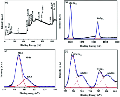 |
| | Fig. 11 (a) XPS survey spectrum of Zn0.98Co0.02O nanoparticles, (b), (c) and (d) high resolution spectra of Zn, O and Co, respectively. | |
The high resolution spectra of Zn 2p, O 1s and Co 2p are given in Fig. 11b, c and d, respectively. Due to strong spin orbit coupling, the Zn 2p peaks have been split into two at 1020.35 eV and 1043.43 eV which can be assigned to the 2p3/2 and 2p1/2 binding states.37 Moreover, the energy difference of ∼23 eV between two peaks is in well agreement with the standard value of ZnO and it strongly indicates the +2 oxidation state of Zn.38 The high resolution O 1s spectra can be resolved into two components at 528.9 eV and 530.4 eV which corresponds to the O2− ions in the Zn0.98Co0.02O lattice (Zn–O, Co–O bonds) and the adsorbed oxygen on the Zn0.98Co0.02O nanopowder surface, respectively.39,40 In the high resolution spectra of Co, the energy difference of ∼16 eV between the energy states confirms the incorporation of cobalt ions into ZnO lattice at +2 oxidation state.41 In addition to the two major peaks at 779.08 eV and 795.7 eV due to spin orbit splitting of cobalt, two satellite peaks located at ∼785 eV and ∼800 eV were appeared. These characteristic peaks also known as shake-up resonance transitions resulted from the transition of valence electrons and core holes.36,40 XPS and XRD investigations concurrently confirms that Co2+ ions have been incorporated into ZnO lattice by substituting Zn2+ ions with no additional phase or impurities.
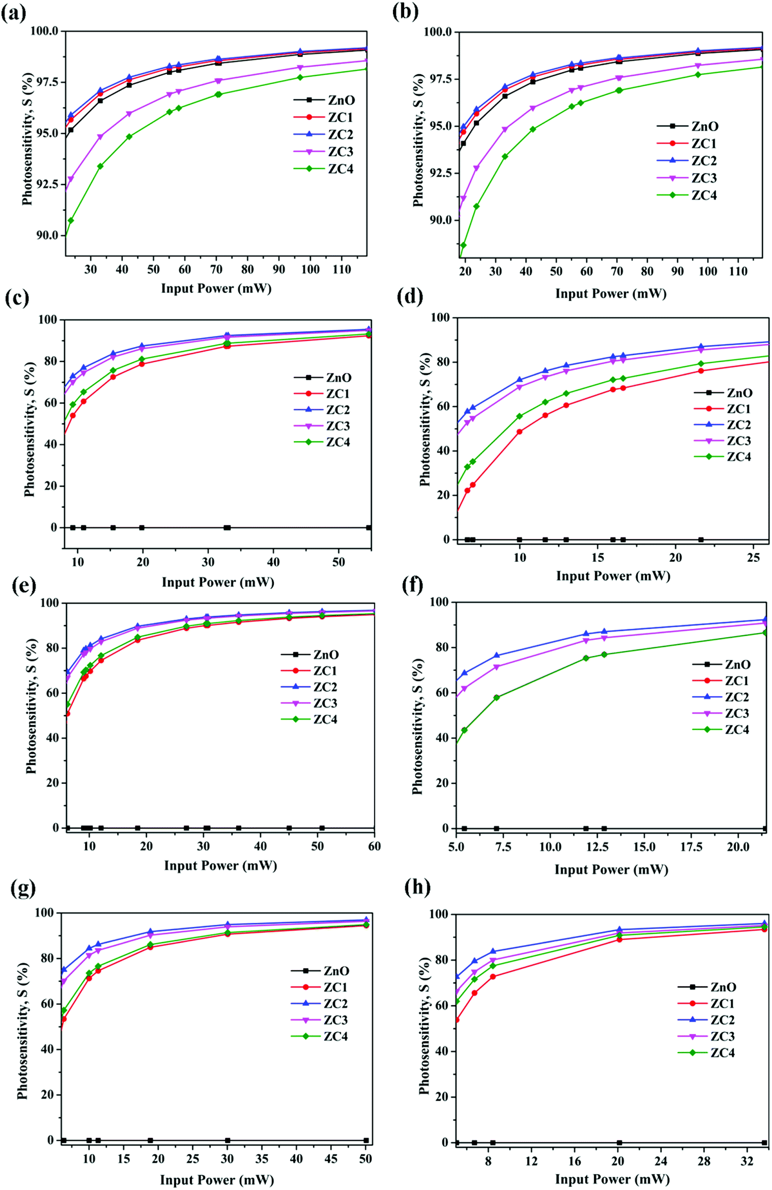
3.2. Photoresponse studies
The photodetection studies of the fabricated PDs were performed under dark, NUV and different visible wavelength light sources. The LEDs were kept at a distance of 4 cm from the PDs biased at 5 V and the photocurrent was measured at different input powers.
The photosensitivity (S) was calculated from the obtained dark and light environment resistance values Rd and Rl, respectively for different source power as,
| |
 | (5) |
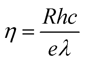
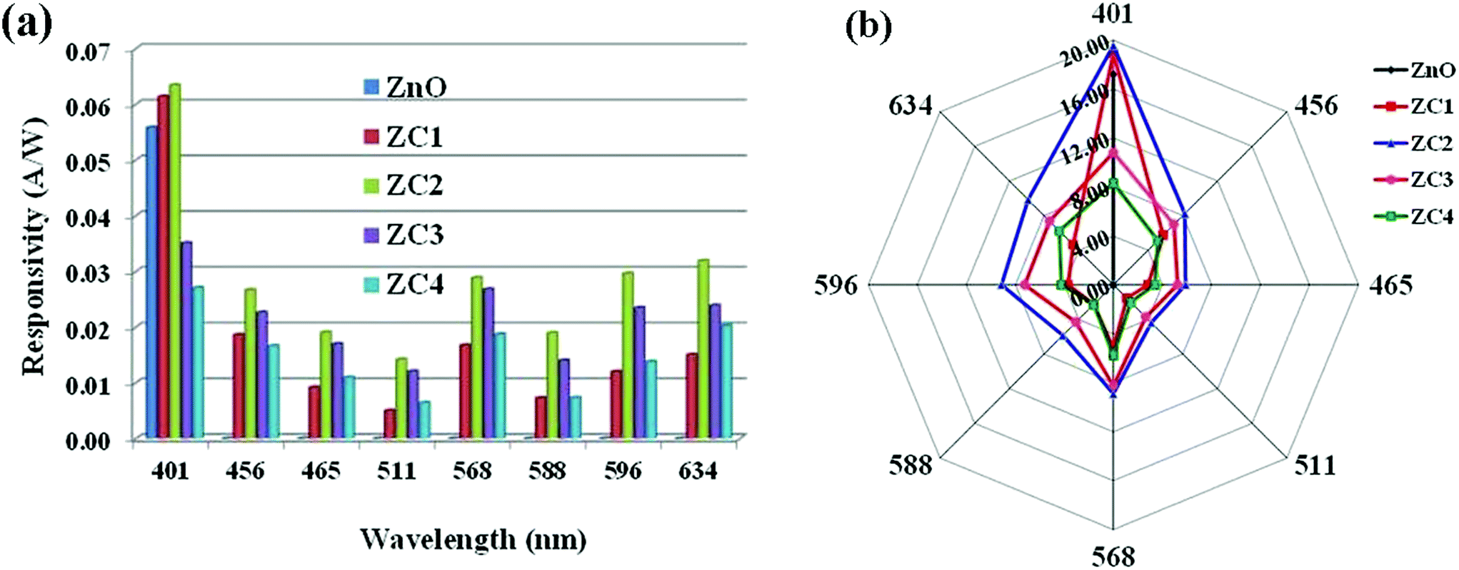
The photoresponse of PDs towards different wavelength was seen to be consistent with the obtained DRS optical response (Fig. 12). The parameters responsivity (R) and quantum efficiency (η) of the PDs at different wavelengths were calculated using the relations,42
| |
 | (6) |
| |
 | (7) |
where,
Id and
Il are the photocurrents under dark and light conditions, respectively.
Pin is the power input to PD,
h is the Plank's constant,
c is the velocity of light,
e is the electron charge and
λ is the source wavelength. The
R and
η values of PDs at different wavelengths are shown in
Fig. 13a and b. In the NUV regime, ZC1 and ZC2 PDs exhibited enhanced photoresponse and increased
η compared to ZnO PD, which is due to the improvement in photoconductivity of ZnO (as seen in
Fig. 10) by doping with smaller concentration of transition metal. Also, due to the shift in absorption edge and presence of absorption bands arose from ligand field split states, appreciable visible light absorption is obtained with Co doping. As expected from the optical spectrum, the visible absorption is increased up until 2% doping of Co and decreased with further increase in concentration. In the visible regime, all the Co doped ZnO PDs showed good response, whereas towards higher wavelengths (>565 nm) the PDs exhibit better response due to the d–d transition of Co
2+ ions. Thus doping with Co at lower concentration can significantly enhance the photoresponsivity of ZnO PDs in NUV and visible regime.
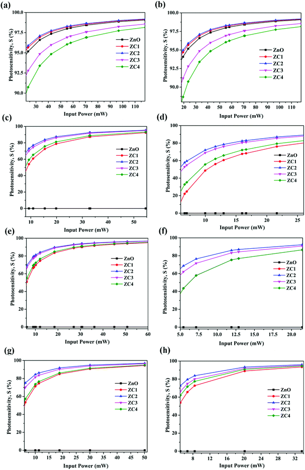 |
| | Fig. 12 Photosensitivity of fabricated PDs towards LED sources (a) 401 nm (b) 456 nm (c) 465 nm (d) 511 nm (e) 570 nm (f) 588 nm (g) 598 nm and (h) 634 nm towards varying input power. | |
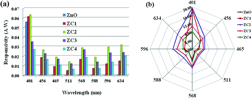 |
| | Fig. 13 (a) Responsivity and (b) quantum efficiency of the fabricated photodetectors. | |
Literature reports show the fabrication of various photodetectors based on ZnO nanostructures with different architectures and synthesis methods. Due to the wide bandgap, pure ZnO itself acts as a good UV detector. Dopants like magnesium,42–45 iron,46 vanadium,47 gallium,48 lanthanum,49 manganese,50 antimony,51 titanium,15 etc., in ZnO have been reported for the improvement of ZnO response in the UV region. When it comes to visible detection, the reports on successful fabrication of visible detectors based on ZnO are very scarce. Our first attempt for the fabrication of ZnO based visible detector was with cadmium (Cd) doping, which red shifted the band gap and extended the detection up to blue region (2.66 eV). But further shifting towards visible region was still not feasible.19 In the present work, Co doping improves detection in multiple visible bands simultaneously with UV, which is a remarkable achievement for the various applications of visible detectors as discussed in the introduction. Merging with other functionalities or technologies like plasmonic enhancement, self-powering, portable PDs which stands on flexible electronics the performance of these detectors can be still improved.49,50,52–58
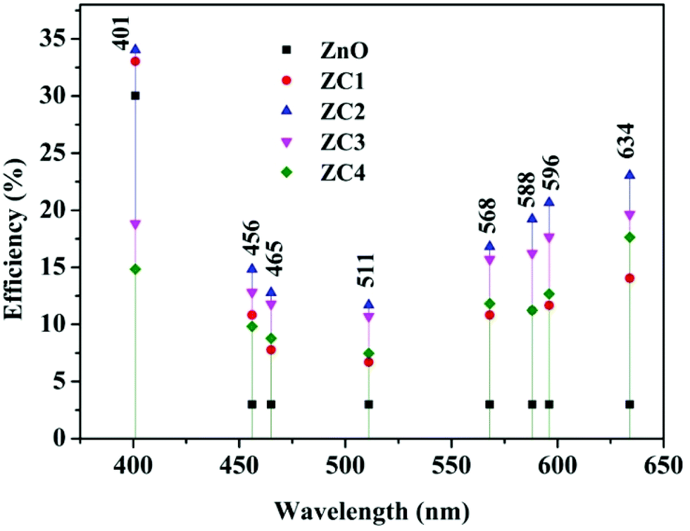
Fig. 14 shows the efficiency of fabricated PDs at different wavelengths. Compared to pure ZnO, an increase of ∼3% and 4% was obtained with ZC1 and ZC2 PDs respectively in the NUV regime. Remarkable visible light response was observed with all PDs, especially at higher wavelengths. Among all, ZC2 PD exhibited higher photoresponse in NUV as well visible region, for which an efficiency of 23% was achieved at 634 nm. These results give a strong foundation for the fabrication of Co doped ZnO NUV-Vis PDs for various applications. Though silicon (1.1 eV) and germanium (0.67 eV) based light detectors are commercially available, the low band gaps lead to undesirable near-IR light response which has to be eliminated and that again complex the architecture and increases the expenditure.59 This study proposes a panacea for the design of efficient visible light detection at multiple energy bands.
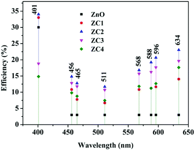 |
| | Fig. 14 Efficiency of fabricated photodetectors. | |
4. Conclusions
Zn1−xCoxO (x = 0, 1, 2, 3 & 4) nanoparticles having hexagonal wurtzite structure were synthesized by co-precipitation method. Upon Co doping in addition to the NUV absorption, broad visible absorptions around ∼571 nm, 618 nm and 682 nm has also been observed due to d–d transition of Co2+ ions. At the Co doping concentration of 1 and 2%, the near UV detection efficiency of PDs was improved by 3–4% and Zn0.98Co0.02O gave a maximum responsivity value of about 63 mA W−1. The Zn1−xCoxO PDs showed good response to visible lights among which x = 2 exhibited maximum efficiency of 23% at 634 nm. Thus, the advantage of ligand field splitting states of Co doped ZnO in the visible region was utilized for the fabrication of ZnO based NUV-Vis PDs. The investigation from this work put forwards that the efficient visible photodetectors with enhanced photoabsorption can be fabricated with Co doped ZnO nanoparticles. Combining with other functionalities or technologies like self-powered PDs, portable PDs with flexible electronics etc., fabrication of still improved visible light PDs can be achieved.
Conflicts of interest
There are no conflicts to declare.
Acknowledgements
The authors would like to acknowledge the Department of Science and technology (DST), New Delhi, India for providing the financial support through FIST (Fund for Improvement of S&T Infrastructure in Higher Educational Institutions) project [SR/FST/ETI-015/2011].
References
- N. Bi, L. Zhang, Q. Zheng, F. Zhuge, J. Li, X. P. Gao and J. Du, J. Mater. Sci. Technol., 2017 DOI:10.1016/j.jmst.2017.03.024.
- M. Cao, F. Wang, J. Zhu, X. Zhang, Y. Qin and L. Wang, Mater. Lett., 2017, 192, 1 CrossRef CAS.
- M. Kahouli, A. Barhoumi, A. Bouzid, A. Al-Hajry and S. Guermazi, Superlattices Microstruct., 2015, 85, 7 CrossRef CAS.
- A. Bedia, F. Z. Bedia, M. Aillerie, N. Maloufi and B. Benyoucef, Energy Procedia, 2015, 74, 529 CrossRef CAS.
- G. H. He, H. Zhou, H. Shen, Y. J. Lu, H. Q. Wang, J. C. Zheng, B. H. Li, C. X. Shan and D. Z. Shen, Appl. Surf. Sci., 2017, 412, 554 CrossRef CAS.
- A. Bedia, F. Z. Bedia, B. Benyoucef and S. Hamzaoui, Electrical characteristics of ultraviolet photodetector based on ZnO nanostructures, Phys. Procedia, 2014, 55, 53 CrossRef CAS.
- Z. Zhang, Q. Liao, Y. Yu, X. Wang and Y. Zhang, Nano Energy, 2014, 9, 237 CrossRef CAS.
- H. Chen, K. Liu, L. Hu, A. A. Al-Ghamdi and X. Fang, Mater. Today, 2015, 18, 493 CrossRef CAS.
- T. Makino, Y. Segawa, M. Kawasaki, A. Ohtomo, R. Shiroki, K. Tamura, T. Yasuda and H. Koinuma, Appl. Phys. Lett., 2001, 78, 1237 CrossRef CAS.
- Y. Wang, J. Chen, S. Yu, E. J. Alcocer, M. Shahid, Z. Wang and W. Pan, Sci. Rep., 2016, 6, 2 CrossRef PubMed.
- N. Nithya and S. R. Radhakrishnan, International Journal of Engineering Research and Technology, 2013, 2, 1649 Search PubMed.
- J. S. Shiau, S. Brahma, C. P. Liu and J. L. Huang, Thin Solid Films, 2016, 620, 170 CrossRef CAS.
- J. D. Hwang, S. Y. Wang and S. B. Hwang, J. Alloys Compd., 2016, 656, 618 CrossRef CAS.
- P. S. Shewale and Y. S. Yu, Ceram. Int., 2016, 42, 7125 CrossRef CAS.
- P. S. Shewale and Y. S. Yu, J. Alloys Compd., 2016, 654, 79 CrossRef CAS.
- L. U. Khan, Digital Communications and Networks, 2017, 3, 78 CrossRef.
- S. Gowrishankar, L. Balakrishnan and N. Gopalakrishnan, Ceram. Int., 2014, 40, 2135 CrossRef CAS.
- N. Kumar and A. Srivastava, J. Alloys Compd., 2017, 706, 438 CrossRef CAS.
- A. A. Jacob, L. Balakrishnan, S. R. Meher, K. Shambavi and Z. C. Alex, J. Alloys Compd., 2017, 695, 3753 CrossRef CAS.
- P. Koidl, Phys. Rev. A, 1977, 15, 2493 CAS.
- V. Y. Ivanov, A. J. Zakrzewski, B. S. Witkowski and M. Godlewski, Opt. Mater., 2016, 59, 15 CrossRef CAS.
- H. Yang and S. Nie, Mater. Chem. Phys., 2009, 114, 279 CrossRef CAS.
- W. Li, G. Wang, C. Chen, J. Liao and Z. Li, Nanomaterials, 2017, 7, 20 CrossRef PubMed.
- C. A. Johnson, A. Cohn, T. Kaspar, S. A. Chambers, G. M. Salley and D. R. Gamelin, Phys. Rev. B: Condens. Matter Mater. Phys., 2011, 84, 125203 CrossRef.
- A. A. Akl and A. S. Hassanien, Int. J. Adv. Res., 2014, 2, 1 Search PubMed.
- M. G. Nair, M. Nirmala, K. Rekha and A. Anukaliani, Mater. Lett., 2011, 65, 1797 CrossRef CAS.
- S. A. Ansari, A. Nisar, B. Fatma, W. Khan and A. H. Naqvi, Mater. Sci. Eng., B, 2012, 177, 428 CrossRef CAS.
- R. He, B. Tang, C. Ton-That, M. Phillips and T. Tsuzuki, J. Nanopart. Res., 2013, 15, 2030 CrossRef.
- M. Shatnawi, A. M. Alsmadi, I. Bsoul, B. Salameh, G. A. Alna'washi, F. Al-Dweri and F. El Akkad, J. Alloys Compd., 2016, 655, 244 CrossRef CAS.
- S. Sakthivel, B. Neppolian, M. V. Shankar, B. Arabindoo, M. Palanichamy and V. Murugesan, Sol. Energy Mater. Sol. Cells, 2003, 77, 65 CrossRef CAS.
- F. Yakuphanoglu, J. Alloys Compd., 2010, 507, 184 CrossRef CAS.
- H. Yang and S. Nie, Mater. Chem. Phys., 2009, 114, 279 CrossRef CAS.
- J. N. Hodgson, Optical absorption and dispersion in solids, Springer Science & Business Media, 2012 Search PubMed.
- W. K. Liu, G. M. Salley and D. R. Gamelin, J. Phys. Chem. B, 2005, 109, 14486 CrossRef CAS PubMed.
- C. A. Johnson, T. C. Kaspar, S. A. Chambers, G. M. Salley and D. R. Gamelin, Phys. Rev. B: Condens. Matter Mater. Phys., 2010, 81, 125206 CrossRef.
- Z. K. Heiba and L. Arda, J. Mol. Struct., 2012, 1022, 167 CrossRef CAS.
- N. L. Tarwal, K. V. Gurav, T. P. Kumar, Y. K. Jeong, H. S. Shim, I. Y. Kim, J. H. Kim, J. H. Jang and P. S. Patil, J. Anal. Appl. Pyrolysis, 2014, 106, 26 CrossRef CAS.
- C. D. Wagner, W. M. Riggs, L. E. Davis, J. F. Moulder and G. E. Mulenberg, Handbook of X-ray Photoelectron Spectroscopy, Perkin–Elmer Co., 1979, p. 82 Search PubMed.
- M. Chen, X. Wang, Y. H. Yu, Z. L. Pei, X. D. Bai, C. Sun, R. F. Huang and L. S. Wen, Appl. Surf. Sci., 2000, 158, 134 CrossRef CAS.
- Y. Zhu, G. Xu, T. Guo, H. Hou and S. Tan, J. Alloys Compd., 2017, 720, 105 CrossRef CAS.
- S. Deka and P. A. Joy, Solid State Commun., 2005, 134, 665 CrossRef CAS.
- P. S. Shewale and Y. S. Yu, J. Alloys Compd., 2016, 654, 79 CrossRef CAS.
- Y. H. Liu, S. J. Young, L. W. Ji, T. H. Meen, C. H. Hsiao, C. S. Huang and S. J. Chang, IEEE Trans. Electron Devices, 2014, 61, 1541 CrossRef CAS.
- Y. H. Liu, S. J. Young, L. W. Ji and S. J. Chang, IEEE J. Sel. Top. Quantum Electron., 2015, 21, 223 CrossRef.
- Y. Hou, Z. Mei and X. Du, J. Phys. D: Appl. Phys., 2014, 47, 283001 CrossRef.
- A. Khayatian, V. Asgari, A. Ramazani, S. F. Akhtarianfar, M. A. Kashi and S. Safa, Mater. Res. Bull., 2017, 94, 77 CrossRef CAS.
- B. B. Deka and A. Misra, ACS Appl. Mater. Interfaces, 2016, 8, 18182 Search PubMed.
- S. S. Shinde and K. Y. Rajpure, Appl. Surf. Sci., 2011, 257, 9595 CrossRef CAS.
- C. L. Hsu, H. H. Li and T. J. Hsueh, ACS Appl. Mater. Interfaces, 2013, 5, 11142 CAS.
- C. O. Chey, X. Liu, H. Alnoor, O. Nur and M. Willander, Phys. Status Solidi RRL, 2015, 9, 87 CrossRef CAS.
- S. V. Mohite and K. Y. Rajpure, Opt. Mater., 2014, 36, 833 CrossRef CAS.
- R. Yang, A. Sazonov and V. Karanassios, in Sensors IEEE, 2016, p. 3 Search PubMed.
- R. Ishimatsu, A. Naruse, R. Liu, K. Nakano, M. Yahiro, C. Adachi and T. Imato, Talanta, 2013, 117, 139 CrossRef CAS PubMed.
- O. Game, U. Singh, T. Kumari, A. Banpurkar and S. Ogale, Nanoscale, 2014, 6, 503 RSC.
- Y. Guo, Y. Li, Q. Zhang and H. Wang, J. Mater. Chem. C, 2017, 5, 1436 RSC.
- G. Gu, N. Mojaverian, J. Vaillancourt and X. Lu, J. Phys. D: Appl. Phys., 2014, 47, 435106 CrossRef.
- H. Wang, J. W. Lim, F. M. Mota, Y. J. Jang, M. Yoon, H. Kim, W. Hu, Y. Y. Noh and D. H. Kim, J. Mater. Chem. C, 2017, 5, 399 RSC.
- S. B. Wang, R. S. Chen, S. J. Chang, H. C. Han, M. S. Hu, K. H. Chen and L. C. Chen, Nanoscale, 2014, 6, 1264 RSC.
- Q. Lin, A. Armin, D. M. Lyons, P. L. Burn and P. Meredith, Adv. Mater., 2015, 27, 2060 CrossRef CAS PubMed.
|
| This journal is © The Royal Society of Chemistry 2017 |
Click here to see how this site uses Cookies. View our privacy policy here. 
 Open Access Article
 This Open Access Article is licensed under a Creative Commons Attribution-Non Commercial 3.0 Unported Licence
 *bc,
K. Shambavid and
Z. C. Alexe
*bc,
K. Shambavid and
Z. C. Alexe