
 Open Access Article
 This Open Access Article is licensed under a
 Creative Commons Attribution 3.0 Unported Licence
Nontoxic (CH3NH3)3Bi2I9 perovskite solar cells free of hole conductors with an alternative architectural design and a solution-processable approach†
Mengqin Kong‡
a,
Hang Hu‡ a,
Li Wan*a,
Miaomiao Chena,
Yisheng Gana,
Jia Wangb,
Fengxiang Chena,
Binghai Donga,
Dominik Ederb and
Shimin Wanga
a,
Li Wan*a,
Miaomiao Chena,
Yisheng Gana,
Jia Wangb,
Fengxiang Chena,
Binghai Donga,
Dominik Ederb and
Shimin Wanga
aHubei Collaborative Innovation Center for Advanced Organic Chemical Materials, Key Laboratory for the Green Preparation and Application of Functional Materials, Ministry of Education, Faculty of Materials Science and Engineering, Hubei University, Wuhan 430062, P. R. China. E-mail: wanli@hubu.edu.cn
bInstitute of Materials Chemistry, Technische Universität Wien, Getreidemarkt 9/165, Vienna 1060, Austria
First published on 17th July 2017
Abstract
Methylammonium iodide bismuthate ((CH3NH3)3Bi2I9) (MBI) perovskite was introduced as a new lead-free and air-stable absorber for hole conductor-free perovskite solar cells. The two-step soaking-assisted sequential solution (2-S) method was adopted to fabricate MBI films for the first time. We compared the formation processes and final morphologies of the MBI films fabricated using the 1-S and 2-S methods on planar and mesoporous TiO2 layers, respectively. We also investigated the effects of the morphologies of MBI films and device architectural design on device performance. Results showed that the MBI films fabricated using the 2-S method achieved a superior coverage both on the compact TiO2 and mesoporous TiO2 layers. The mesoporous structure devices presented higher power conversion efficiencies than the planar structure devices. In addition, all devices exhibited excellent thermal and long-term stabilities. The presented architectural design and solution-processable approach could inspire further research and practical applications on lead-free organic–inorganic hybrid perovskite solar cells.
1. Introduction
Organic–inorganic hybrid perovskite solar cells have recently generated considerable attention and research interest for photovoltaic applications because of their low cost, solution processability, and high-developing device efficiencies. To date, the power conversion efficiency (PCE) of hybrid lead-based perovskite solar cells (PSCs) has exceeded 22%.1 However, lead-based PSCs are facing significant challenges of lead toxicity and intrinsic instability, which have raised great concerns on the long-term environmental impact and human health,2–4 seriously hindering their commercialization.3 Therefore, finding a suitable substitution for lead compounds with nontoxic analogs and comparable photovoltaic properties has been a diligent and emergent task for researchers.Sn and Ge analogs, which are under the same group 14 as Pb, are viable alternative materials for lead perovskites. Relative to the widely used methylammonium lead triiodide (MAPbI3) perovskites, Sn and Ge compounds show numerous similarities in optoelectronic properties and photosensitivity. The Sn perovskite CH3NH3SnI3 has achieved a moderate PCE of over 6%.5 However, the intrinsic unstable Sn2+ ions within the material are easily oxidized to Sn4+ because Sn normally prefers the tetravalent state.5–8 Meanwhile, Ge-based perovskite displays poor ability to form a homogeneous film, and Ge analogs that contain active lone pair electrons are more easily oxidized than Sn2+.9 As a result, Ge-based PSCs exhibit poor photocurrent densities and a PCE of 0.2%.10 These negative features decrease the reproducibility and performance of the devices, limiting their practical application. Other promising derivatives for Pb-free alternatives are Sb or Bi perovskites, which are group 15 elements. However, limited information is available about the photovoltaic properties of Sb-based compounds. Planar heterojunction solar cells based on a (CH3NH3)3Sb2I9 absorber material have recently been studied,11 but the (CH3NH3)3Sb2I9 film provides an incomplete coverage on the substrate surface, yielding a low photocurrent density. As a result, the PCE of the device is still low (approximately 0.5%).
Recent studies have demonstrated that 0D Bi-based compounds12–18 with the chemical formula (CH3NH3)3Bi2I9 (MBI) are suitable for photosensitive layer in solar cells.19–27 Bi-Based perovskites have been previously subjected to experimental and theoretical analyses.28,29 However, little is known about the photovoltaic properties of these Bi-based compounds. The potential semiconducting character, nontoxicity, and excellent stability in the humid atmosphere20–22 of Bi-based compounds have aroused considerable interest from researchers. Bi3+ cation has the outer lone pair of 6s2 electrons, which can improve stability.30,31 Hoye et al.19 showed that MBI is a promising photovoltaic absorber from the experimental and theoretical perspectives. MBI is a nontoxic material and is more stable than lead-based perovskites because of the formation of a small amount of either Bi2O3 or BiOI on its surface layer. These properties overcome the two main bottlenecks of hybrid lead-based perovskites in future commercial application. Lyu et al.20 fabricated MBI-based PSCs with a PCE of ∼0.19%, and the devices can maintain very limited performance degradation after 21 days of storage in ambient air, exhibiting excellent long-term stability. Moreover, Singh and Zhang et al. conducted a comprehensive study on MBI-based PSCs with planar and mesoporous structures, obtaining PCEs of 0.2% (ref. 25) and 0.42% (ref. 27) both on TiO2 mesoscopic architecture, respectively. However, almost all of the fabrication processes of MBI films involved the one-step spin-coating (1-S) method, and only Hoye et al.19 and Ran et al.24 fabricated MBI films through using a two-step sequential spin-coating method and a two-step evaporation-spin-coating method, respectively. The former MBI films were fabricated on borosilicate glass and quartz substrates instead of assembling into any devices. In the latter case, the inverted planar heterojunction device obtained a best PCE of 0.39%.
In the present work, the two-step soaking-assisted sequential solution (2-S) method was introduced for the first time to fabricate MBI films. We compared the formation processes and final morphologies of the MBI films fabricated using the 1-S and 2-S methods on planar and mesoporous TiO2 layers, respectively. Results confirmed that the compact TiO2 layer (cp-TiO2) plays a vital role in charge transporting, collecting photoelectrons, and inhibiting the recombination of electron and hole effectively.32 Therefore, the cp-TiO2 layer is an important component of the MBI-based PSCs. In the present study, magnetron sputtering was used to prepare the cp-TiO2 layer, which can facilely achieve the uniformity of TiO2 thin films and improve the reproducibility of device performance. The MBI films fabricated using the 2-S method achieved a superior coverage both on the cp-TiO2 and mesoporous TiO2 (mp-TiO2) layers. In addition, MBI-based PSCs based on free-hole-transporting material architecture have not been reported. Thus, we fabricated a commercial carbon paste to form a counter electrode by the blade coating method, thereby enhancing the stability and reducing the overall costs of the devices.33–36 We assembled these MBI films into hole conductor-free PSCs in ambient air with the structures of FTO/cp-TiO2/MBI/C and FTO/cp-TiO2/mp-TiO2/MBI/C, and then investigated the effects of the morphologies of MBI films and device architecture on device performance.
2. Experimental details
2.1 MBI films fabrication
A 1-S MBI precursor solution was formed by BiI3 (99.99%, Aladdin) and CH3NH3I (MAI, 99%, MaterWin) mixture with a molar ratio of 1![[thin space (1/6-em)]](https://www.rsc.org/images/entities/char_2009.gif) :1.5 in 1 mL of N,N-dimethylformamide (DMF, 99.8%, Sigma-Aldrich) solvent. A 1 mol L−1 1-S MBI precursor solution was deposited on top of the TiO2 film (cp-TiO2 or mp-TiO2 layers) by spin coating at 6000 rpm for 30 s, followed by heating at 100 °C for 30 min on an annealing plate.
:1.5 in 1 mL of N,N-dimethylformamide (DMF, 99.8%, Sigma-Aldrich) solvent. A 1 mol L−1 1-S MBI precursor solution was deposited on top of the TiO2 film (cp-TiO2 or mp-TiO2 layers) by spin coating at 6000 rpm for 30 s, followed by heating at 100 °C for 30 min on an annealing plate.
The 2-S method was conducted similar to the formation of CH3NH3PbI3. First, a 1 mol L−1 BiI3 solution in DMF was spin coated at 6000 rpm for 30 s on the cp-TiO2 or mp-TiO2 layers, obtaining a BiI3 film transformed from reddish into black after heating at 100 °C for 10 min. Then, the black BiI3 film was soaked in a 10 mg mL−1 MAI solution dissolved in isopropanol (99.5%, Sigma-Aldrich), followed by heating at 100 °C for 30 min on an annealing plate. After a while, the film changed to reddish immediately, indicating the formation of the MBI perovskite film (Fig. 1).
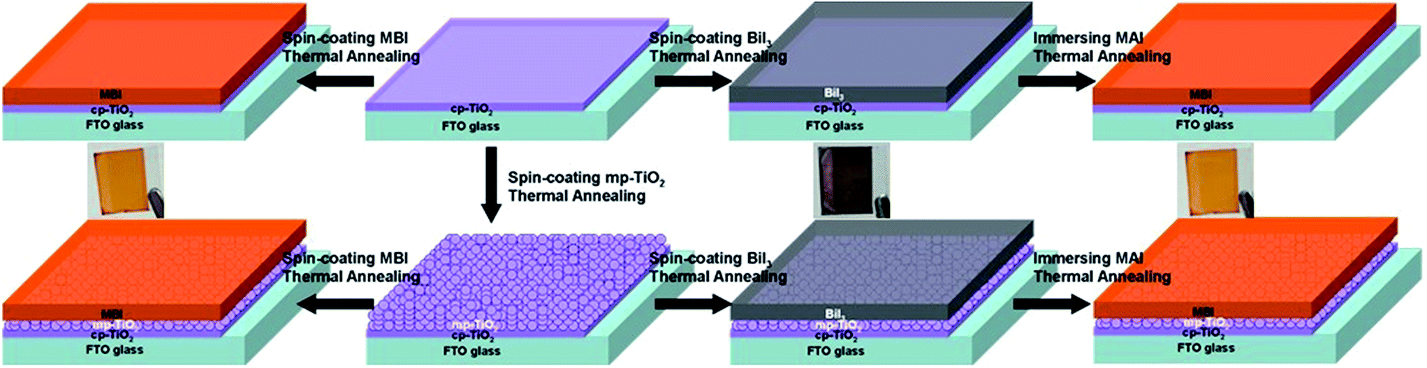 | ||
| Fig. 1 Scheme of the fabrication process of the MBI layer based on the cp-TiO2 and mp-TiO2. | ||
2.2 Fabrication of solar cell
FTO-coated glass (sheet resistance 14 Ω cm−1, Jinge) substrates were cleaned by ultrasonication for 20 min in detergent, deionized water, acetone, ethanol, and isopropanol, successively. The cp-TiO2 layer was deposited onto the cleaned FTO substrates by direct-frequency magnetron sputtering (DFMS). The TiO2 target (with 99.99% purity) was sputtered under a power of 100 W for 30 min. DFMS was performed with the TRP-450 system (SKY Technology Development Co., Ltd., CAS) in pure Ar gas (99.999%). The coated TiO2 films were annealed at 500 °C for 15 min. For the preparation of the mp-TiO2 layer, the commercial TiO2 paste (18-NRT, MaterWin) was also deposited by spin coating at 3000 rpm on top of the cp-TiO2 layer for 30 s followed by annealing at 550 °C for 1 h. The MBI layer was fabricated as described above. On the basis of the cp-TiO2 (mp-TiO2) substrate, the BiI3 thin films fabricated using the 2-S method were termed cp-BiI3 and mp-BiI3. Similarly, the MBI thin films fabricated using the 1-S (2-S) method were termed 1-cp-MBI (2-cp-MBI) and 1-mp-MBI (2-mp-MBI). Finally, the counter electrode of carbon (JELCON CH-8 carbon ink, sheet resistance 10 Ω cm−1, JUJO Printing Supplies & Technology (Pinghu) Co., Ltd., China) was fabricated by a blade-coating method on top of the reddish MBI films.2.3 Characterization
The X-ray diffraction (XRD) data of the BiI3 and MBI films based on the cp-TiO2 and mp-TiO2 substrates were collected with a Bruker-AXS D8 Advance using Cu Kα radiation ranging from 10° to 60° (2θ) at room temperature. The cross-section of the cells and the morphologies of the BiI3, MBI, cp-TiO2, and mp-TiO2 films were observed via field-emission scanning electron microscopy (FE-SEM, Jeol JEM 6510LV) and atomic force microscopy (AFM, Nanoscope-IIIa). The roughness of the films was determined by AFM. The absorption of the MBI film was recorded using UV-vis spectrophotometry (UV-3600, Shimadzu). X-ray photoelectron spectroscopy (XPS, Thermo Fisher) was conducted on a Scientific Escalab 250Xi instrument with monochromatized Al K-Alpha radiation. Thermo gravimetric analysis (TGA) of the MBI powder sample was performed using Discovery TGA (PERKIN ELMER, USA). The current–voltage (I–V) curves of the devices were measured under simulated AM 1.5G (100 mW cm−2 irradiance) using the solar simulator (Oriel, model 91192-1000) and the model digital source meter (Keithley 2400, USA). Electrochemical impedance spectroscopy (EIS) was conducted by an electrochemical workstation (Zennium, IM6, Germany) over the frequency from 10 mHz to 2 MHz under simulated AM 1.5G (100 mW cm−2 irradiance). The surface-wetting properties of carbon surfaces in a full cell were evaluated via the static contact angles measurement employing a Dataphysics OCA 30 (Dataphysics, Germany) contact angle system at room temperature.3. Results and discussion
X-ray photoelectron spectroscopy (XPS) was performed on the MBI monocrystal powder to confirm the elemental composition and valence of the near-surface atoms. Fig. S1(a)† shows the prospective peaks of Bi, I, N, C, and O. As shown in Fig. 2(a), two XPS peaks were observed, which originated from the methylammonium cation (MA+) at binding energies of 286 and 284.58 eV, which corresponded to C–N and C–C bonds.23,26 The N 1s (402 eV) signal originating from the MA+ is shown in Fig. 2(b). The peaks for I 3d3/2 (630.68 eV) and 3d5/2 (619.18 eV) (Fig. 2(c)), Bi 4f5/2 (164.18 eV) and Bi 4f7/2 (158.88 eV) (Fig. 2(d)) can be attributed to the characteristic signals from I− and Bi3+ species, respectively. Scans of the Bi 4f indicated that Bi was mainly in the 3+ oxidation state. In addition, the binding energy of the Bi 4f7/2 peak can be attributed to both Bi–O and Bi–I bonds. The surface O 1s spectrum of MBI fitted with a 530.5 eV binding energy peak corresponding to O–Bi, and another peak at 531.58 eV originated from the adsorbed surface species (Fig. S1(b)†).19 These results indicated that O–Bi occurred on the MBI surface after a period of air exposure, thus forming a surface oxygen-based species.19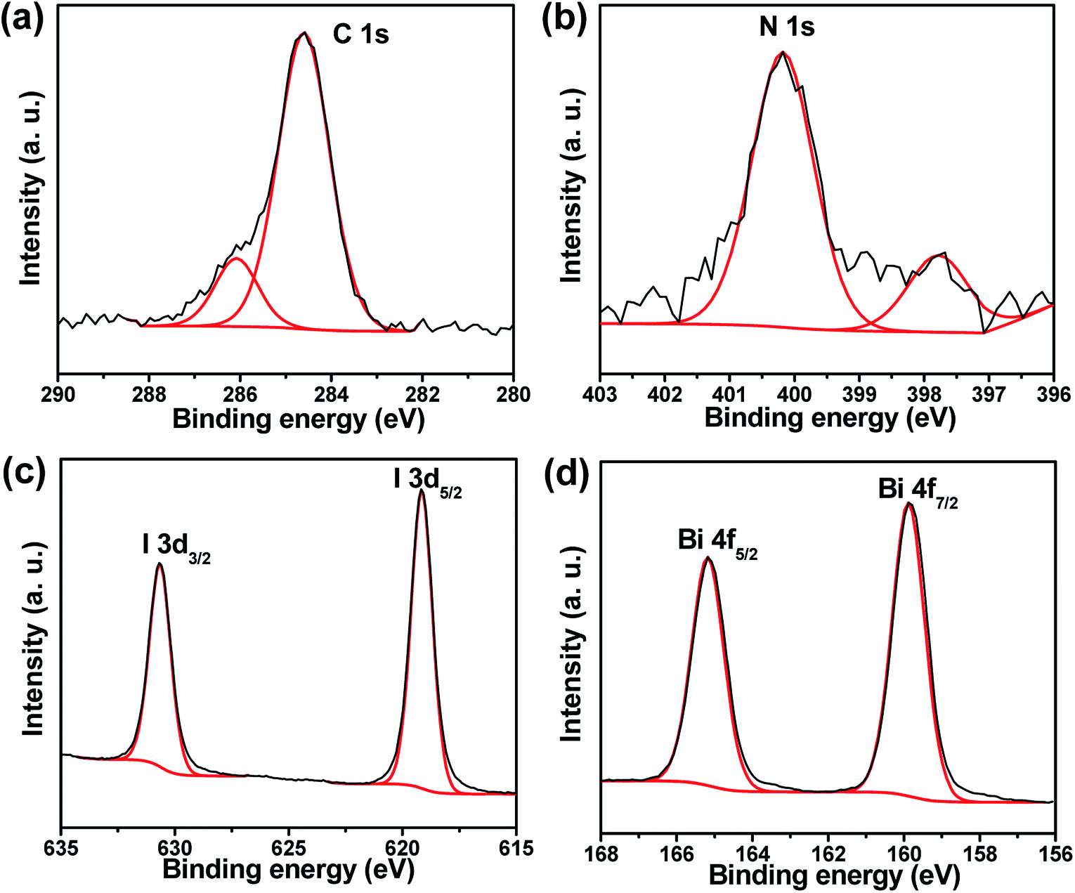 | ||
| Fig. 2 The high resolution XPS spectra of (a) C 1s, (b) N 1s, (c) I 3d, and (d) Bi 4f for MBI monocrystal powder. | ||
The XRD patterns of different BiI3 and MBI films onto the mp-TiO2 or cp-TiO2 substrate are shown in Fig. 3(a). Four main peaks of cp-BiI3 and mp-BiI3 films at 2θ from 10° to 60° were observed. In the XRD patterns of MBI films, all samples of the diffraction peaks were consistent with literature reports,20,27 suggesting that MBI belongs to the hexagonal system with the P63/mmc space group.20,37 The results agreed well with the hexagonal morphology of MBI single crystals as shown in Fig. S2.† In addition, other diffraction peaks of BiI3 were not detectable in all the MBI film samples, indicating that almost all BiI3 has been transformed completely into MBI.
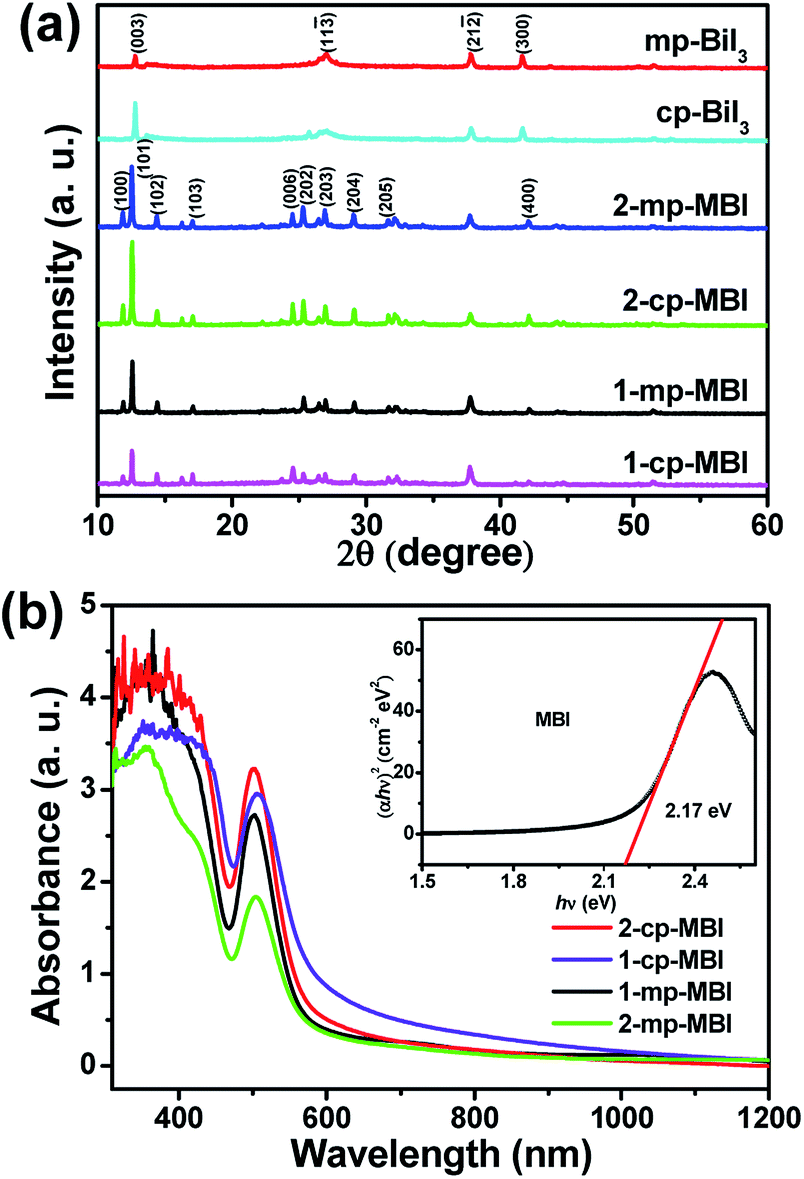 | ||
| Fig. 3 (a) XRD patterns of different BiI3 and MBI films. (b) Absorption spectrum of different MBI films. Inset: Tauc plots for the MBI thin film. | ||
The optical absorption spectra showed an edge at approximately 600 nm in all MBI samples (Fig. 3(b)), and the 1-cp-MBI samples exhibited the highest absorption. The absorptions of the MBI thin films based on planar TiO2 substrates (1-cp-MBI and 2-cp-MBI) were both higher than those of the mesoporous MBI samples (1-mp-MBI and 2-mp-MBI) because of the thinner corresponding TiO2 layers. The transmission-mode absorption spectrum of the MBI thin films displayed as Tauc plots (inset) suggests an indirect band gap of 2.17 eV.
Fig. 4 shows the surface morphology of the MBI perovskite layer fabricated by different methods on the planar and mesoporous TiO2 layers. As shown in Fig. 4(a)–(d), all the hexagonal MBI crystals displayed irregular orientation on top of the TiO2 layer. The surface morphologies of the MBI thin films spin coated using the 1-S method (Fig. 4(a) and (b)) differed from those of the MBI thin films spin coated using the 2-S method. For the MBI thin films fabricated using the 2-S method (Fig. 4(c) and (d)), hexagonal MBI crystalline grains with sizes of hundreds of nanometers were randomly stacked, whereas MBI crystalline grains closely conjoined with a mass of unfilled holes for the MBI thin films fabricated with the 1-S method. The morphological differences can be attributed to the different crystallization rates and fabrication processes of the MBI thin films under the 1-S and 2-S methods. The MBI layer fabricated by the 2-S method was transformed from the BiI3 thin film, which contributed to the morphology of the MBI layer. The surface morphology of the BiI3 layer is shown in Fig. S3.† The BiI3 thin film exhibited non-uniform coverage along with consecutive cracks on top of the TiO2 layer.
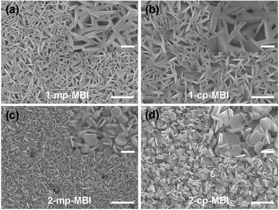 | ||
| Fig. 4 Top-view FE-SEM images of the MBI perovskite layer: (a) 1-mp-MBI, (b) 1-cp-MBI, (c) 2-mp-MBI and (d) 2-cp-MBI. The insets are the high resolution images, and the scale bars on the images and the insets are 2 μm and 500 nm, respectively. | ||
This study compared the planar and mesoporous architecture of solar cells and the morphologies of the 1-S and 2-S methods for fabricating MBI films. AFM was used to characterize the topography and surface roughness of the perovskite film. Fig. 5(a)–(h) show typical AFM 2D images of the TiO2, BiI3, and MBI films based on the planar and mesoporous architecture by the 1-S and 2-S methods. The root-mean-square roughnesses (Rrms) of the cp-TiO2 and mp-TiO2 substrates were calculated to be 10.456 and 20.080 nm, respectively, indicating that the surface of the mp-TiO2 layer was bumpier than that of the cp-TiO2 layer. In theory, the topography of TiO2 nanoparticles with a bumpy surface affects the surface uniformity of MBI films. As a result, the mp-BiI3 (20.615 nm) and 2-mp-MBI (43.269 nm) films were bumpier than the cp-BiI3 (17.863 nm) and 1-mp-MBI (30.720 nm) films (Fig. 6), respectively. However, an exception exists for this case. The surface roughness of the 1-cp-MBI film fabricated using the 1-S method based on the planar TiO2 substrate reached a maximum value of Rrms (107.489 nm), which was in accordance with the result shown in Fig. 4(b).
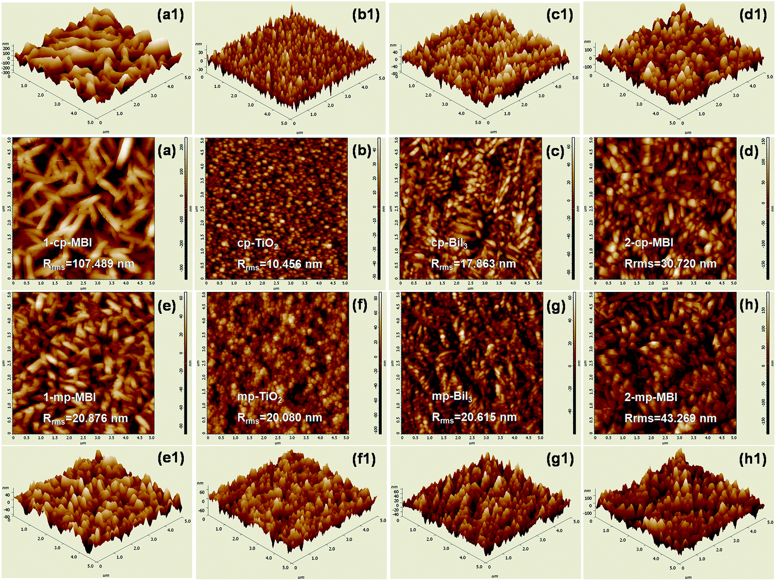 | ||
| Fig. 5 (a) to (h) AFM 2D topography images and (a1) to (h1) 3D views of the TiO2, BiI3, and MBI films. | ||
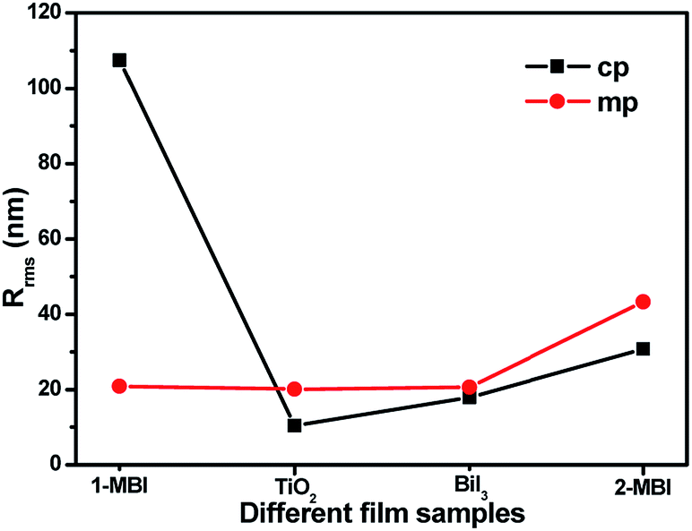 | ||
| Fig. 6 Dependence of Rrms of different thin films on planar and mesoporous structure. | ||
Fig. 7(a) shows the energy level diagram of the device. All the energy levels were obtained from aforementioned studies.27,32 MBI exhibited a p-type semiconductor characteristic and a colossal potential as an absorber in solar cell. The energy levels for the conduction band (CB) and valence band (VB) edges of MBI were at −3.8 and −5.9 eV, with a good match of the TiO2 energy levels of CB (−4.1 eV) and VB (−7.3 eV), respectively. Meanwhile, carbon had a Fermi level at −5.0 eV, and served as the hole collection layer. The cross-section FE-SEM images (Fig. 7(d) and (e)) of the devices illustrate unfilled voids partially emerged on the MBI/C interface because of the bumpy surface morphology of the MBI film and layered carbon material, which resulted in a weak attachment of the MBI perovskite layer to the carbon counter electrode. The thickness of the MBI layer based on planar structure was approximately 600 nm (Fig. 7(d)), whereas the total thickness of the mp-TiO2 layer and MBI capping layer was approximately 1 μm (Fig. 7(e)). A carbon counter electrode with a thickness of approximately 5.2 μm can be observed (Fig. S4†). We employed the commercial carbon paste (Fig. S5(a)†) to form a counter electrode (CE) by blade coating method and its composition is shown in the Table S1.† In addition, the surface of the carbon is hydrophobic (Fig. S5(b)†). The contact angle for H2O on carbon surfaces in a full cell was 101°, implying that the hydrophobic carbon surface may be conducive to prevent the moisture from reaching the underlying MBI layer. Thus this approach can further improve the long-term stability of the whole devices without encapsulation.
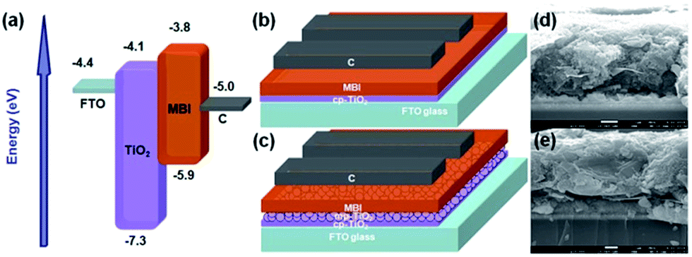 | ||
| Fig. 7 (a) Energy level diagram of the HTM-free PSCs. (b) and (c) Schematic illustration of devices with the planar and mesoporous structures. (d) and (e) Cross-sectional FE-SEM image of the overall planar and mesoporous devices, both of the scale bars on the images are 1 μm. | ||
The photovoltaic performance of the devices based on different MBI films and device architecture was tested under AM 1.5G irradiation (100 mW cm−2). Compared with MAPbI3, MBI exhibited a superior stability in ambient atmosphere. Thus, we conducted all material and device processing in ambient air. The J–V curves of these PSC devices are shown in Fig. 8, and the corresponding photovoltaic parameters are summarized in Table 1. On the one hand, the mesoporous structure devices (1-mp and 2-mp) presented higher PCEs at around 0.05% compared with the planar structure devices (1-cp and 2-cp). Notably, the 1-mp devices exhibited the best PCE of 0.054%, which was attributed to the high open-circuit voltage (Voc) of 895 mV. On the other hand, the planar structure device (1-cp) fabricated by the 1-S method exhibited a higher PCE at 0.039% compared with that (2-cp) fabricated by the 2-S method. The 2-cp device presented a low PCE of 0.017% as the results of the low short-circuit current density (Jsc) (0.131 mA cm−2) and Voc (514 mV). The low photocurrent of the devices possibly resulted from the large intrinsic indirect band gap of MBI,27 which limits the improvement of device performance.20,27 In addition, the PSC device with a hole conductor-free layer and a carbon counter electrode exhibited a relatively low fill factor (FF), which can be attributed to the weakened attachment of the MBI layer to the carbon counter electrode.
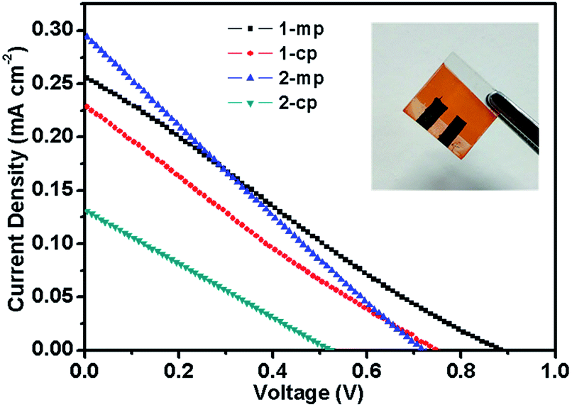 | ||
| Fig. 8 J–V characteristics of PSCs based on different device architecture and MBI-fabricated method under simulated AM 1.5G (100 mW cm−2 irradiance). The inset is an actual image of a device. | ||
| Samples | Voc (mV) | Jsc (mA cm−2) | FF (%) | PCE (%) |
|---|---|---|---|---|
| 1-mp | 895 | 0.255 | 24.0 | 0.054 |
| 1-cp | 755 | 0.230 | 23.0 | 0.039 |
| 2-mp | 715 | 0.298 | 24.2 | 0.052 |
| 2-cp | 514 | 0.131 | 25.8 | 0.017 |
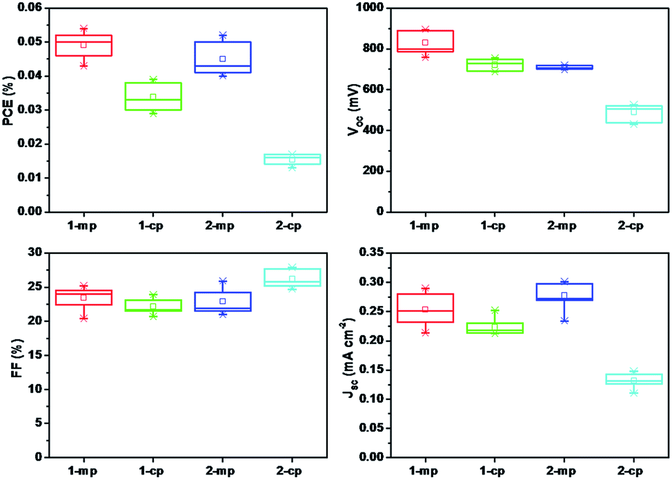
To check the reproducibility of the device performance, one batch of devices (seven separate devices) based on different MBI films as absorbers were obtained under the same experimental conditions. The distribution of the corresponding photovoltaic parameters are exhibited in Fig. 9 and the average values summarized in Table S2.† The PCEs of the best device (1-mp) ranged from 0.046% to 0.054% with a average value of 0.049%, and most of the devices had a PCE of approximately 0.05%. Meanwhile, all 1-mp devices had a Voc value greater than 750 mV. In addition, the average PCEs of 2-mp, 1-cp and 2-cp were 0.045%, 0.034% and 0.015%, respectively. These results indicated the good reproducibility of the devices.
 | ||
| Fig. 9 Histograms of photovoltaic parameters for 7 devices based on different device architecture and MBI-fabricated method under simulated AM 1.5G (100 mW cm−2 irradiance). | ||
In order to further understand the relationship between architecture effect and charge transport behavior in the hole conductor-free PSCs, we performed electrochemical impedance spectroscopy (EIS) measurements on these devices over the frequency range of 10 mHz to 2 MHz at 0.2 V bias under simulated AM 1.5G (100 mW cm−2 irradiance). In a typical hole conductor-free PSC device with an architecture of TiO2/perovskite/CE, there are two contact interfaces: TiO2/perovskite and perovskite/CE, respectively.32 In our study, two interfaces of TiO2/MBI and MBI/C were taken into account and a equivalent circuit model is shown in the inset of Fig. 10. As shown in Fig. 10, two arcs can be observed for all of these devices: the first arc at the high-frequency region corresponds to the charge transfer resistance (Rtr) at the MBI/C interface, while the second arc at the low-frequency region is associated with the recombination resistance (Rrec) at the MBI/TiO2 interface. The fitting parameters of the experimental data are given in Table 2. The series resistance (Rs) of the four devices were basically close to around 115 Ω, in good agreement with the similar value of FF.38 The mesoporous devices (1-mp and 2-mp) had a similar Rtr value of about 230 Ω, and were smaller than that of planar devices (1-cp: 270.4 Ω, 2-cp: 290.0 Ω). This indicates that the MBI nanocrystal filling into mp-TiO2 layer probably enhanced the interface attachment of MBI layer to the C layer that is closely related to the MBI morphology, thus increasing the efficiency of collection or extraction of photogenerated holes at the MBI/C interface. Furthermore, the mesoporous devices had both larger Rrec (1-mp: 1085.0 Ω, 2-mp: 1107.0 Ω) compared to the planar devices (1-cp: 701.7 Ω, 2-cp: 656.3 Ω), which can reduce the rate of electron–hole recombination at the MBI/TiO2 interface. As a result, the mesoporous devices with low Rtr and high Rrec reached superior performance matching the J–V characteristics (Fig. 8 and 9).
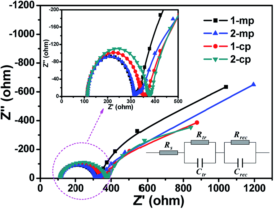 | ||
| Fig. 10 Nyquist curves of the PSCs based on different device architecture and MBI-fabricated method under simulated AM 1.5G (100 mW cm−2 irradiance) with a bias of 0.2 V. The inset is a equivalent circuit. | ||
| Samples | Rs (Ω) | Rtr (Ω) | Rrec (Ω) |
|---|---|---|---|
| 1-mp | 114.5 | 230.5 | 1085.0 |
| 1-cp | 114.3 | 270.4 | 701.7 |
| 2-mp | 115.9 | 232.5 | 1107.0 |
| 2-cp | 115.7 | 290.0 | 656.3 |
To explore the cause of the thermodynamic stability of MBI, thermo gravimetric analysis (TGA) was performed on MBI, BiI3, and CH3NH3I powders in a nitrogen atmosphere (Fig. 11(a) and (b)). As shown in the TGA curve of CH3NH3I, the onset of mass loss emerged at ∼250 °C followed by 100% mass loss at 320 °C, in which the decomposition products were HI and CH3NH2. BiI3 underwent a sharp mass loss at 350–400 °C, suggesting the sublimation of BiI3. Therefore, the TGA curve of MBI indicated that the initial mass loss at 250 °C can be attributed to the vaporization of CH3NH2 and decomposition of HI because of the 5.61% and 23.18% mass losses of MBI, respectively.19,39 Moreover, MBI exhibited the remaining mass loss at 350–400 °C during the sharp transition of the second step because of the sublimation of BiI3. Another TGA measurement in an inert atmosphere showed a similar feature with parallel trends, thus proving the excellent thermal stability of MBI absorbers.
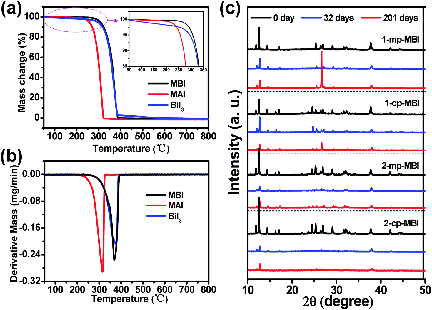 | ||
| Fig. 11 (a) TGA and (b) DTG heating curves of MBI, MAI and BiI3 powders. (c) XRD patterns of different MBI films after storage in ambient air for 0 day, 32 days and 201 days, respectively. | ||
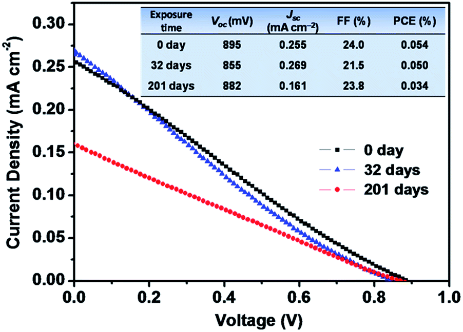
We further assessed the air stability of the MBI film based on the cp-TiO2 or mp-TiO2 layer through XRD measurements. The MBI films were stored in ambient air (approximately 40% humidity) for 0, 32, 201 days. The MBI films remained reddish after 32 days, only becoming slightly brighter after storage for 201 days. Fig. 11(c) shows that the XRD patterns of MBI remained mostly unchanged instead of degrading to diffraction peaks of BiI3. These results suggest that MBI is in a superior stable phase after long-term exposure to ambient air.19 Importantly, the PCE decay measurements were carried out on the devices, and further revealed that the MBI film played a pivotal role in the device stability. As shown in Fig. 12, the champion device (1-mp) still yielded a PCE of 0.05% (i.e., it maintained 92.6% of its initial PCE) after storaged in ambient air for 32 days. On continuous exposure to ambient air for 201 days, the 1-mp device exhibited 63.0% of its initial PCE, which was attributed to the drop of Jsc from 0.255 to 0.161 mA cm−2. Other cell samples exhibited parallel trends of PCE decay. Therefore, all results indicate that these PSCs exhibited excellent long-term stability.
 | ||
| Fig. 12 J–V characteristics of PSCs based on 1-mp device under simulated AM 1.5G (100 mW cm−2 irradiance), which was measured after 0, 32, and 201 days, respectively. | ||
4. Conclusions
MBI perovskite was introduced as a new lead-free absorber for hole conductor-free PSCs. The 2-S method was adopted to fabricate MBI films for the first time. The MBI films fabricated using the 2-S method achieved a superior coverage both on the cp-TiO2 and mp-TiO2 layers. Furthermore, the performance of PSCs was found to depend on MBI film morphology and device architectural design. The mesoporous structure devices presented higher PCEs at around 0.05% than the planar structure devices. All the devices exhibited excellent thermal and long-term stabilities. Creating high-quality, homogeneous, and compact MBI thin films is an effective strategy to further improve device performance. With this lead-free and nontoxic MBI perovskite, the low-temperature solution methods developed in this study could be used to prepare MBI thin films on planar and mesoporous TiO2 substrates, which may stimulate further research and practical applications.Acknowledgements
This work was supported by the National Natural Science Foundation of China (51572072 and 21402045). This work was also financially supported by Wuhan Science and Technology Bureau of Hubei Province of China (2013010602010209), Educational commission of Hubei Province of China (D20141006) and Department of Science & Technology of Hubei Province of China (2015CFA118).Notes and references
- Best Research-Cell Efficiencies, http://www.nrel.gov/ncpv/images/efficiency_chart.jpg.
- A. Babayigit, D. Duy Thanh, A. Ethirajan, J. Manca, M. Muller, H.-G. Boyen and B. Conings, Sci. Rep., 2016, 6, 18721 CrossRef CAS PubMed.
- A. Babayigit, A. Ethirajan, M. Muller and B. Conings, Nat. Mater., 2016, 15, 247–251 CrossRef CAS PubMed.
- I. R. Benmessaoud, A.-L. Mahul-Mellier, E. Horváth, B. Maco, M. Spina, H. A. Lashuel and L. Forró, Toxicol. Res., 2016, 5, 407–419 RSC.
- N. K. Noel, S. D. Stranks, A. Abate, C. Wehrenfennig, S. Guarnera, A.-A. Haghighirad, A. Sadhanala, G. E. Eperon, S. K. Pathak, M. B. Johnston, A. Petrozza, L. M. Herz and H. J. Snaith, Energy Environ. Sci., 2014, 7, 3061 CAS.
- M. H. Kumar, S. Dharani, W. L. Leong, P. P. Boix, R. R. Prabhakar, T. Baikie, C. Shi, H. Ding, R. Ramesh, M. Asta, M. Graetzel, S. G. Mhaisalkar and N. Mathews, Adv. Mater., 2014, 26, 7122–7127 CrossRef CAS PubMed.
- F. Hao, C. C. Stoumpos, D. H. Cao, R. P. H. Chang and M. G. Kanatzidis, Nat. Photonics, 2014, 8, 489–494 CrossRef CAS.
- E. S. Parrott, R. L. Milot, T. Stergiopoulos, H. J. Snaith, M. B. Johnston and L. M. Herz, J. Phys. Chem. Lett., 2016, 7, 1321–1326 CrossRef CAS PubMed.
- M. Zhang, M. Lyu, P. Chen, M. Hao, J.-H. Yu and L. Wang, Asia-Pac. J. Chem. Eng., 2016, 11, 392–398 CrossRef CAS.
- T. Krishnamoorthy, H. Ding, C. Yan, W. L. Leong, T. Baikie, Z. Zhang, M. Sherburne, S. Li, M. Asta, N. Mathews and S. G. Mhaisalkar, J. Mater. Chem. A, 2015, 3, 23829–23832 CAS.
- J.-C. Hebig, I. Kühn, J. Flohre and T. Kirchartz, ACS Energy Lett., 2016, 1, 309–314 CrossRef CAS.
- B. Liu, L. Xu, G.-C. Guo and J.-S. Huan, J. Solid State Chem., 2006, 179, 1611–1617 CrossRef CAS.
- M. R. Filip, S. Hillman, A.-A. Haghighirad, H. J. Snaith and F. Giustino, J. Phys. Chem. Lett., 2016, 7, 2579–2585 CrossRef CAS PubMed.
- N. Leblanc, N. Mercier, M. Allain, O. Toma, P. Auban-Senzier and C. Pasquier, J. Solid State Chem., 2012, 195, 140–148 CrossRef CAS.
- C. Hrizi, N. Chaari, Y. Abid, N. Chniba-Boudjada and S. Chaabouni, Polyhedron, 2012, 46, 41–46 CrossRef CAS.
- H. Dammak, A. Yangui, S. Triki, Y. Abid and H. Feki, J. Lumin., 2015, 161, 214–220 CrossRef CAS.
- A. J. Lehner, D. H. Fabini, H. A. Evans, C.-A. Hébert, S. R. Smock, J. Hu, H. Wang, J. W. Zwanziger, M. L. Chabinyc and R. Seshadri, Chem. Mater., 2015, 27, 7137–7148 CrossRef CAS.
- G. Volonakis, M. R. Filip, A. A. Haghighirad, N. Sakai, W. Bernard, H. J. Snaith and F. Giustino, J. Phys. Chem. Lett., 2016, 7, 1254–1259 CrossRef CAS PubMed.
- R. L. Z. Hoye, R. E. Brandt, A. Osherov, V. Stevanović, S. D. Stranks, M. W. B. Wilson, H. Kim, A. J. Akey, J. D. Perkins, R. C. Kurchin, J. R. Poindexter, E. N. Wang, M. G. Bawendi, V. Bulović and T. Buonassisi, Chem.–Eur. J., 2016, 22, 2605–2610 CrossRef CAS PubMed.
- M. Lyu, J.-H. Yun, M. Cai, Y. Jiao, P. V. Bernhardt, M. Zhang, Q. Wang, A. Du, H. Wang, G. Liu and L. Wang, Nano Res., 2016, 9, 692–702 CrossRef CAS.
- B.-W. Park, B. Philippe, X. Zhang, H. Rensmo, G. Boschloo and E. M. J. Johansson, Adv. Mater., 2015, 27, 6806–6813 CrossRef CAS PubMed.
- Y. Qiu, W. Liu, W. Chen, W. Chen, G. Zhou, P.-C. Hsu, R. Zhang, Z. Liang, S. Fan, Y. Zhang and Y. Cui, Sci. Adv., 2016, 2, e1501764 Search PubMed.
- D. M. Fabian and S. Ardo, J. Mater. Chem. A, 2016, 4, 6837–6841 CAS.
- C. Ran, Z. Wu, J. Xi, F. Yuan, H. Dong, T. Lei, X. He and X. Hou, J. Phys. Chem. Lett., 2017, 8, 394–400 CrossRef CAS PubMed.
- T. Singh, A. Kulkarni, M. Ikegami and T. Miyasaka, ACS Appl. Mater. Interfaces, 2016, 8, 14542–14547 CAS.
- S. Öz, J.-C. Hebig, E. Jung, T. Singh, A. Lepcha, S. Olthof, J. Flohre, Y. Gao, R. German, P. H. M. Loosdrecht, K. Meerholz, T. Kirchartz and S. Mathur, Sol. Energy Mater. Sol. Cells, 2016, 158, 195–201 CrossRef.
- X. Zhang, G. Wu, Z. Gu, B. Guo, W. Liu, S. Yang, T. Ye, C. Chen, W. Tu and H. Chen, Nano Res., 2016, 9, 2921–2930 CrossRef CAS.
- T. Kawai and S. Shimanuki, Phys. Status Solidi, 1993, 177, K43–K45 CrossRef CAS.
- T. Kawai, A. Ishii, T. Kitamura, S. Shimanuki, M. Iwata and Y. Ishibashi, J. Phys. Soc. Jpn., 1996, 65, 1464–1468 CrossRef CAS.
- L. M. Schoop, L. Muchler, C. Felser and R. J. Cava, Inorg. Chem., 2013, 52, 5479–5483 CrossRef CAS PubMed.
- R. E. Brandt, V. Stevanović, D. S. Ginley and T. Buonassisi, MRS Commun., 2015, 5, 265–275 CrossRef CAS.
- H. Hu, B. Dong, H. Hu, F. Chen, M. Kong, Q. Zhang, T. Luo, L. Zhao, Z. Guo, J. Li, Z. Xu, S. Wang, D. Eder and L. Wan, ACS Appl. Mater. Interfaces, 2016, 8, 17999–18007 CAS.
- C. Y. Chan, Y. Wang, G. W. Wu and E. W. Diau, J. Mater. Chem. A, 2016, 4, 3872–3878 CAS.
- Z. Liu, T. Shi, Z. Tang, B. Sun and G. Liao, Nanoscale, 2016, 8, 7017–7023 RSC.
- H. Chen, Z. Wei, H. He, X. Zheng, K. S. Wong and S. Yang, Adv. Energy Mater., 2016, 6, 1502087 CrossRef.
- H. Li, K. Cao, J. Cui, S. Liu, X. Qiao, Y. Shen and M. Wang, Nanoscale, 2016, 8, 6379–6385 RSC.
- K. Eckhardt, V. Bon, J. Getzschmann, J. Grothe, F. M. Wisser and S. Kaskel, Chem. Commun., 2016, 52, 3058–3060 RSC.
- E. J. Juarez-Perez, M. Wuβler, F. Fabregat-Santiago, K. LakusWollny, E. Mankel, T. Mayer, W. Jaegermann and I. Mora-Sero, J. Phys. Chem. Lett., 2014, 5, 680–685 CrossRef CAS PubMed.
- A. Dualeh, P. Gao, S. Il Seok, M. K. Nazeeruddin and M. Grätzel, Chem. Mater., 2014, 26, 6160–6164 CrossRef CAS.
Footnotes |
| † Electronic supplementary information (ESI) available: Additional XPS spectrum of MBI monocrystal powder, low-resolution SEM image of single crystals of MBI, SEM image of mp-BiI3 and cp-BiI3 layers, cross-sectional FE-SEM image of the devices, contact angles for H2O on carbon surfaces, the composition of the carbon paste, and summarized device parameters of different devices. See DOI: 10.1039/c7ra04924b |
| ‡ These authors contributed equally to this work. |
| This journal is © The Royal Society of Chemistry 2017 |