
 Open Access Article
 This Open Access Article is licensed under a
 Creative Commons Attribution 3.0 Unported Licence
Relationship between the dipole moment of self-assembled monolayers incorporated in graphene transistors and device electrical stabilities†
Gwang Mo Kua,
Eunho Leeb,
Boseok Kangb,
Jung Hun Leea,
Kilwon Chob and
Wi Hyoung Lee *a
*a
aDepartment of Organic and Nano System Engineering, Konkuk University, Seoul 143-701, Korea. E-mail: whlee78@konkuk.ac.kr; Fax: +82-2-457-8895; Tel: +82-2-450-3468
bDepartment of Chemical Engineering and Center for Advanced Soft Electronics, Pohang University of Science and Technology, Pohang 790-784, Korea
First published on 22nd May 2017
Abstract
Surface characteristics of the gate-dielectric layers in graphene field-effect transistors (FETs) critically affect the electrical properties of the devices. In this report, the effects of self-assembled monolayers (SAMs) on the electrical properties of graphene FETs were examined by using various SAM buffer layers with different end groups and alkyl chain lengths. Especially, the dipole moment of the SAMs affects the doping properties of graphene as well as field-effect mobility, hysteresis, and stability of graphene FETs. The type and magnitude of doping are dependent on the functional groups in SAMs: Electron withdrawing fluorine groups p-dope the graphene whereas electron donating amine groups n-dope the graphene. The electrical stabilities such as hysteresis and gate-bias instability are mainly governed by the magnitude of the dipole moment in SAMs. Hexamethyldisilazane treatment resulted in graphene FETs with the highest electrical stabilities, because of the short one aliphatic alkyl chain with a negligible dipole moment. In contrast, in graphene FETs with SAMs having a strong dipole moment, electrical stabilities deteriorated by the charge trapping in SAMs.
1. Introduction
Graphene has received considerable attention as a future material in display and semiconductor research.1–5 Especially, the development of a synthesis method of large-area/high-quality graphene by chemical vapor deposition (CVD) opens the possibility of graphene for use in future display elements such as transparent conductive electrodes.6–8 Graphene devices have typically been fabricated on SiO2/Si substrates for the device applications of graphene. However, impurities on a SiO2 surface induce charged impurity scattering, thereby decreasing the charge carrier mobility of graphene field-effect transistors (FETs).9,10 In this regard, several research groups have utilized hydrophobic self-assembled monolayers (SAMs) to screen these charged impurities.11–15 For instance, octadecyltrichlorosilane (ODTS) SAMs have been proven to protect charged impurities on a SiO2 surface and reduce the substrate-induced doping of graphene.11–13 The surface protection with ODTS SAMs thereby leads to high charge carrier mobilities with nearly zero Dirac point voltage. However, stability issues including hysteresis and bias stability of the graphene FETs that are fabricated on SAM modified SiO2/Si substrates have not been fully examined yet. Addressing the stability issues of the graphene FETs would contribute to the commercialization of graphene-based devices.Effects of the underlying SAM buffer layers on the electrical properties of graphene FETs have been partially studied. Yokota et al. found that the dipole moment of SAMs induces shift in the Fermi level of graphene, thereby leading to doping of graphene.16 In contrast, electron donating characteristic of NH2-SAMs was shown to induce n-doping of grapheme, because of the charge transfer in graphene/NH2-SAMs interface.17–20 These results indicated that the charge carriers (i.e., electron and hole) in the graphene channel were affected by the SAMs on SiO2/Si substrates. A recent report by Gholamrezaie et al. revealed that the threshold voltage in organic FETs was closely related to the dipole moment in SAMs.21 The surface potential of SAM modified SiO2/Si after the delamination of the deposited organic semiconductor matched well with the observed threshold voltage shift. This result indicates that charge carriers can be trapped at the SAMs mainly, because of the dipole moment in SAMs.
In this study, we examined the effects of the dipole moment of SAMs on the electrical stabilities of graphene transistors. Three different SAM agents were used with different end functional groups and alkyl chain lengths: ODTS, 3-aminopropyltriethoxysilane (APS), and 1H,1H,2H,2H-perfluorodecyl-triethoxysilane (FDTS). Hexamethyldisilazane (HMDS) with one alkyl chain length was compared together. These molecules were self-assembled on a SiO2 surface to construct a uniform molecular layer. The CVD grown graphene was transferred on the SAM modified SiO2/Si substrates, and their electrical stabilities were analyzed by measuring current–voltage hysteresis curves and bias-induced device stability.
2. Experimental
Graphene was synthesized on a Cu foil by the CVD method.6,8 Predominant single layer graphene (>95%) was used in this study. Silicon wafer with thermally grown SiO2 (thickness of 300 nm) was cleaned with acetone, isopropanol, and UV/ozone prior to use. ODTS, APS, and FDTS were self-assembled on SiO2/Si substrates by the dipping method.22 In contrast, HMDS was spin-coated on SiO2/Si substrate followed by baking at 150 °C for 1 h.11 The surface energies of the SAMs-modified SiO2/Si were measured by the contact angle method. Dipole moments of SAMs were measured by ultraviolet photoelectron spectroscopy (UPS; He I source, hν = 21.2 eV) at the 4D beamline of the Pohang Accelerator Laboratory in Korea. The synthesized graphene on Cu foil was transferred on the SAMs-modified SiO2/Si substrates using PMMA (Mw of 996 kg mol−1) supporting layer. Ammonium persulfate with a concentration of 0.05 mol L−1 was used for etching the Cu foil. After the successful transfer of graphene, the PMMA layer was etched by dipping the PMMA/graphene/SAMs-modified SiO2/Si in acetone for 5 h. The optical properties of graphene films were measured by Raman spectroscopy at room temperature using a 532 nm laser (Witec alpha 300R) and G-band and 2D-band were analyzed from the Raman spectra. To fabricate graphene transistors, 50 nm thick Au source/drain electrodes were thermally evaporated on the graphene films through a shadow mask. The channel length and width were 150 and 1500 μm, respectively. Electrical properties of graphene transistors were characterized using a Keithley 4200-SCS under vacuum. Bias stabilities of graphene transistors were measured at the continuous bias condition (VG = −80 V, VD = 0.01 V) for 1 h by monitoring the source/drain current.3. Results and discussion
Fig. 1 shows the schematic showing the self-assembled structures of SAMs used in this study. Despite the same end group (–CH3), HMDS and ODTS SAMs exhibited different wetting properties. HMDS showed a water contact angle of 66°, whereas ODTS showed a water contact angle of 104°. This is attributed to the dense packing of ODTS SAMs induced by its longer alkyl chains.11,23 HMDS does not fully cover the silanol groups on a SiO2 surface, showing a moderate contact angle. The water contact angles of APS and FDTS SAMs were measured to be 50 and 107°, respectively, because of different end group characteristics such as hydrophilicity of the amine groups and hydrophobicity of fluorine atoms.22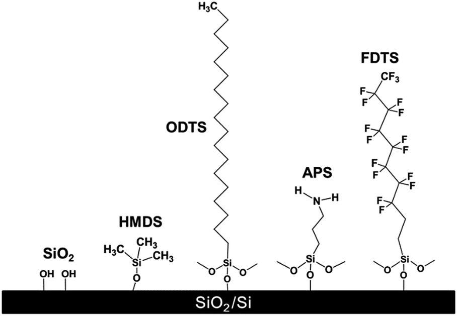 | ||
| Fig. 1 Schematics of self-assembled monomers (SAMs) on SiO2/Si substrates. SiO2: untreated SiO2/Si, HMDS: hexamethyldisilazane treated, ODTS: octadecyltrichlorosilane treated, APS: 3-aminopropyltriethoxysilane treated, and FDTS: 1H,1H,2H,2H-perfluorodecyl-triethoxysilane treated. | ||
To measure the relative direction and magnitude of the dipole moments of SAMs, secondary electron cut off spectra in UPS were measured (Fig. 2). The onset of the secondary electrons is determined by the dipole moment in SAMs.24 The onset of the secondary electrons at a kinetic energy is ordered as follows: FDTS > untreated SiO2 > HMDS > ODTS > APS. The electron withdrawing character of fluorine atoms in FDTS SAMs is responsible for the higher onset kinetic energy compared to that of the untreated SiO2. In contrast, ODTS and APS SAMs exhibit the opposite direction of onset kinetic energy because of the electron donating characteristic of the functional groups (–NH2, –CH3). When comparing ODTS and APS SAMs, the dipole moment of APS SAMs (−1.0 eV) is larger than that of ODTS SAMs (−0.6 eV). HMDS exhibits a very small dipole moment compared to that of ODTS mainly because of the shorter alkyl chain length. The reason for the dipole moment (−0.6 eV) in ODTS SAMs is that ODTS SAMs are constructed on the SiO2 surface in an ordered manner by the hydrophobic interaction between long alkyl chains.23 From the UPS measurement, the direction and magnitude of the dipole moment could be evaluated, and their effects on graphene FETs was investigated.
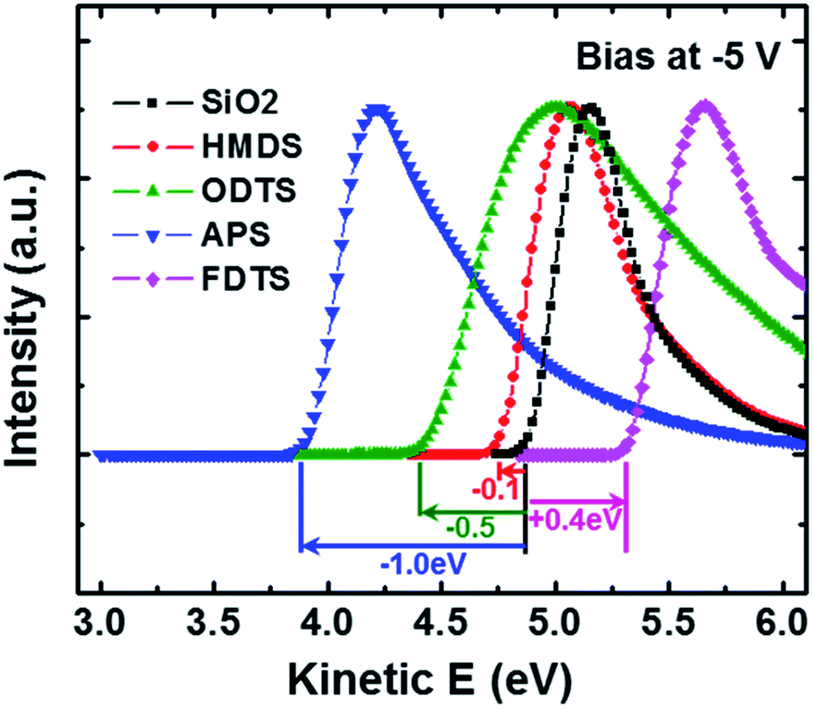 | ||
| Fig. 2 Secondary electron emission spectra of the SiO2/Si substrates treated with various SAMs. | ||
Fig. 3 shows the electrical properties of various graphene FETs prepared with different SAMs inserted between the graphene and SiO2. Gate bias was swept from −80 V to 80 V at a fixed source-drain bias of 0.01 V. Because the impurities from air atmosphere affect the electrical properties of graphene, in situ annealing at 100 °C was optionally conducted in the probe station chamber to exclude this effect. The electrical properties (i.e., electron and hole mobilities, Dirac point voltage, and hysteresis properties) were extracted from the transfer curves and listed in Tables 1 and 2. The graphene FETs on the untreated SiO2 only exhibited p-type characteristics with a low field-effect mobility of 954 cm2 V−1 s−1. The Dirac point voltage therein was not detected in the swept range of the gate voltage up to 80 V. In our experiment, the observed p-type doping of graphene on SiO2 is caused by the adsorbates on SiO2. Adsorbates such as H2O and/or O2 can reside on the hydrophilic SiO2 surface, contributing to p-doping of graphene.25,26 Raman spectra in the ESI Fig. S1† also support a significant p-doping of graphene on a SiO2/Si substrate. The position of G-band in graphene supported on SiO2 is located at 1592 cm−1, which is blue-shifted from the pristine graphene in the literatures.11,17 Although annealing at 100 °C is known to remove atmospheric impurities, adsorbates at the interface between graphene and SiO2 could not be fully removed. For this reason, p-doping of graphene was not changed, and ambipolar properties of graphene were not attained even after thermal annealing at 100 °C.
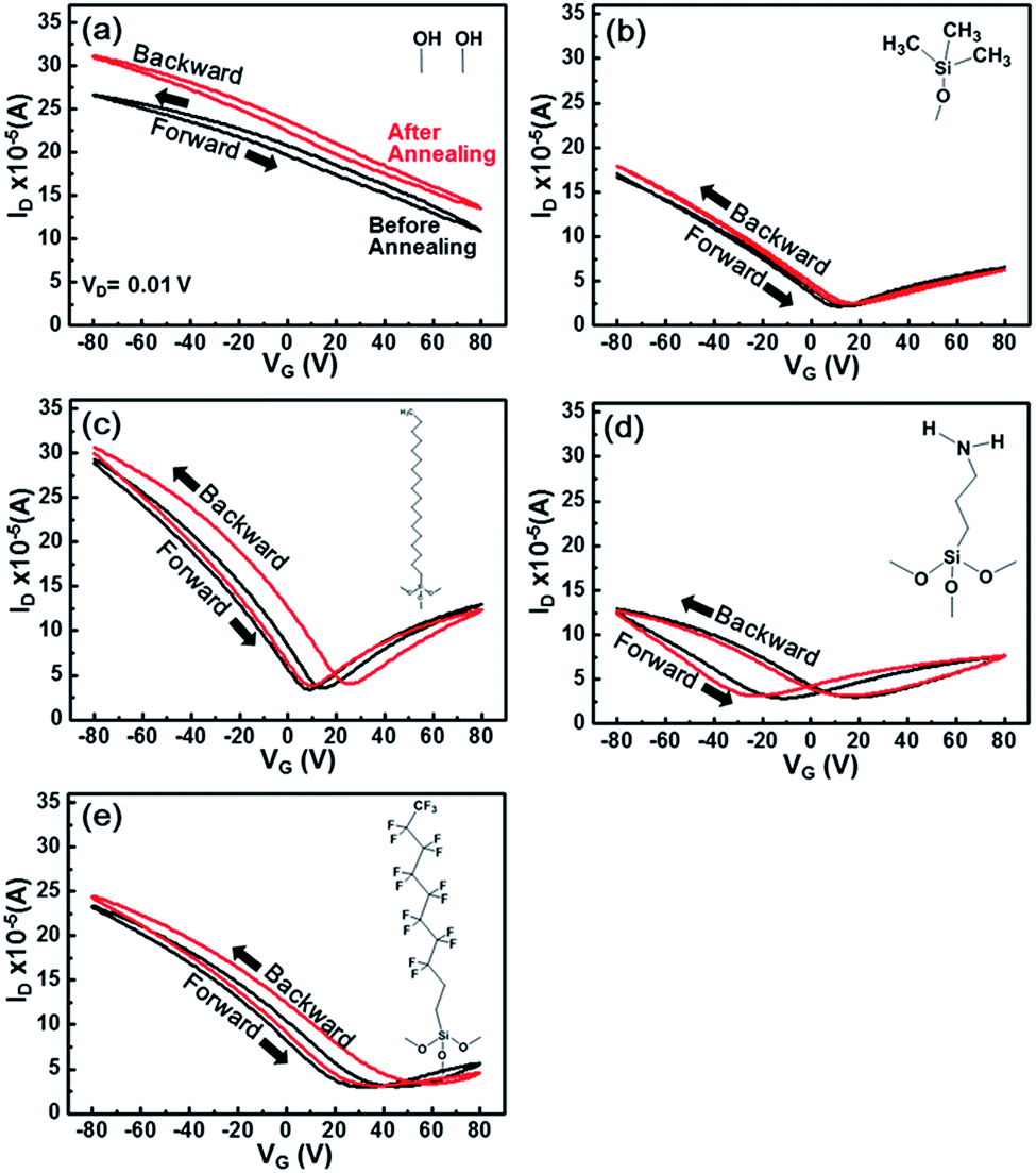 | ||
| Fig. 3 Transfer curves of graphene transistors on various SAMs-modified SiO2/Si substrates before (black line) and after annealing at 100 °C (red line): (a) SiO2/Si, (b) HMDS, (c) ODTS, (d) APS, and (e) FDTS. Bias of VGS = –80 V and VDS = 0.01 V were applied on the graphene transistors. | ||
| μ (p-type) [cm2 V−1 s−1] | μ (n-type) [cm2 V−1 s−1] | VDirac [V] | ΔVmaxhysteresis [V] | |
|---|---|---|---|---|
| APS | 1460 | 588 | −11 | 29 |
| FDTS | 2330 | 569 | 32 | 14 |
| HMDS | 1770 | 806 | 11 | 4 |
| ODTS | 3410 | 843 | 9 | 6 |
| SiO2 | 954 | — | — | — |
The HMDS-modified SiO2 surface showed the recovery of the ambipolar properties of graphene at a Dirac point voltage of 11 V (Fig. 3b). The recovered ambipolarity is due to the passivation of the SiO2 surface with a hydrophobic HMDS layer.14 The increase in the field-effect mobility is directly linked with the suppression of graphene doping caused by the blocking of the charged impurities on the SiO2 surface. In addition, negligible hysteresis was observed in dual sweeps. Because HMDS has a negligible dipole moment, it does not increase the charge trapping in the graphene channel. Accordingly, the graphene FETs with HMDS buffer layer exhibited the smallest hysteresis in dual sweeps. When the ODTS SAMs was used as a buffer layer, the electron and hole mobilities increased more, and the Dirac point voltage is near to zero (Fig. 3c). Because ODTS is self-assembled on the SiO2 surface in an ordered manner, it can block the charged impurities much more effectively than HMDS.11 In contrast, the magnitude of hysteresis increased in the dual sweeps and annealing boosted the hysteresis behaviour, as confirmed by the maximum gate voltage shift in dual sweeps (Tables 1 and 2). We proposed that the increased hysteresis is related to the dipole moment in ODTS SAMs (Fig. 2). Annealing at 100 °C could remove the atmospheric impurities while inducing the intimate contact of graphene on ODTS SAMs. Accordingly, the effects of the dipole moment on the hysteresis behaviours of charge carriers increased after thermal annealing at 100 °C.
| μ (p-type) [cm2 V−1 s−1] | μ (n-type) [cm2 V−1 s−1] | VDirac [V] | ΔVmaxhysteresis [V] | |
|---|---|---|---|---|
| APS | 1690 | 594 | −22 | 38 |
| FDTS | 1950 | 239 | 38 | 21 |
| HMDS | 1810 | 681 | 15 | 3 |
| ODTS | 3570 | 1760 | 10 | 16 |
| SiO2 | 972 | — | — | — |
Graphene FETs prepared with APS SAMs showed n-doping behaviour in the forward sweep (Fig. 3d), corresponding well with the previous reports.17,19,20,27–29 The lone pair electrons in the amine groups have electron donating characteristic, thereby leading to the up-shift of Fermi level (n-doping). In addition, the large dipole moment of APS SAMs triggers a considerable hysteresis in the dual sweeps. The maximum gate voltage shift in APS SAMs increased from 29 V to 38 V after thermal annealing at 100 °C (Tables 1 and 2). Graphene FETs with FDTS-modified SiO2/Si substrates showed the opposite doping behaviour. The Dirac point voltage located at 32 V and can be explained by the dipole moment and the electron withdrawing character of FDTS SAMs. The direction of the dipole moment in FDTS SAMs is opposite to those of ODTS and APS SAMs. Meanwhile, the magnitude of the dipole moment is ordered as follows: APS > ODTS ∼ FDTS. This order matches well with the magnitude of hysteresis in the dual sweeps. Annealing the graphene FETs modified with APS, FDTS, and ODTS SAMs increased the magnitude of hysteresis except for the graphene FETs with HMDS buffer layer showing an opposite trend. We surmise that dipole moment in SAMs is the main reason for the charge trapping triggered hysteresis behaviours, and annealing at 100 °C increased the effects of dipole moment in APS, FDTS, and ODTS SAMs by inducing intimate contact of graphene to these SAMs. On the other hand, HMDS have a negligible dipole moment, and thus annealing at 100 °C decreased the magnitude of hysteresis by removing impurities under the atmospheric conditions.
Fig. 4 shows the gate bias stabilities of graphene FETs with different buffer layers inserted between graphene and SiO2. A prolonged gate bias of −80 V was applied on the devices, and current decay was measured at a source-drain bias of 0.01 V. The on-current levels of all the devices showed decreased, resulting from the charge trapping.30 The graphene FETs on the untreated and those with HMDS treated SiO2 exhibited relatively small current decays. The graphene FETs with FDTS, ODTS, and APS SAMs showed considerable current decays. Especially, graphene FETs with APS SAMs showed the highest current decay (i.e., the lowest degree of bias stability). Amine groups with electron donating characteristics increase the hole trapping when continuous negative gate bias is applied on the devices.
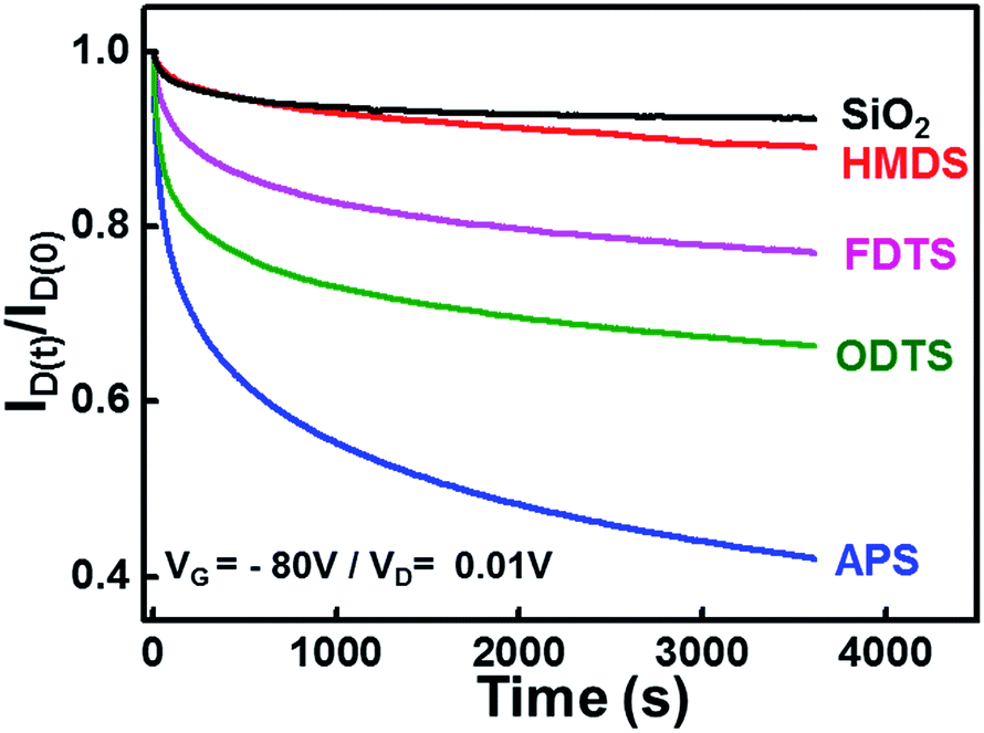 | ||
| Fig. 4 Bias stability of graphene transistors with various SAMs-modified SiO2/Si substrates. Bias of VGS = −80 V and VDS = 0.01 V were applied on the graphene transistors for 60 min. | ||
It is noteworthy that graphene FETs with ODTS SAMs showed a low degree of gate bias stability despite the high electron and hole mobility values. ODTS SAMs have been considered as the most efficient buffer layer for blocking the charged impurities on SiO2 surface and favoring electron and hole transports.11 Note that long alkyl chains in ODTS SAMs contribute to the formation of well-ordered close-packed monolayers by the hydrophobic interactions between the neighboring alkyl chains. On the other hand, ODTS SAMs intrinsically contain dipole moment, inducing trapping of charge carriers. The charge trapping in ODTS SAMs resulted in bias instability and considerable hysteresis. The FETs with a HMDS buffer showed outstanding stability comparable to the untreated SiO2 and can be understood in terms of the chemical structure of HMDS with one alkyl chain. The alkyl chain length dependence of bias stability has been reported in the earlier reports by Suemori et al. and Roh et al., where organic semiconductors were adopted as an active layer.31,32 They found that the trap creation in SAMs with longer alkyl chains (i.e., ODTS) is much more facilitated than SAMs with shorter alkyl chains (i.e., HMDS). However, they could not find physical origins for the observed behaviour. We insist that the dipole moment in SAMs is responsible for the physical origin of the low electrical stabilities. This explanation is in line with a recent study reporting SAM-induced charge trapping in organic FETs.21 To support this claim, we also measured the bias stability of organic FETs with SAMs by using pentacene as an active layer (see the ESI, Fig. S2†). In accordance with the graphene FETs, pentacene FETs with ODTS SAMs resulted in low bias stability under continuous gate-bias. We thus concluded that the electrical instability of graphene FETs with a SAM buffer layer originates from the charge trapping in SAMs, and the SAM-induced charge trapping phenomena are general irrespective of semiconductor materials used.
4. Conclusions
The effects of the dipole moment in SAMs on the electrical properties of graphene FETs were investigated. The secondary electron cut off spectra revealed that the magnitude and direction of dipole moment were determined by the chemical structures of SAMs (i.e., end group and alkyl chain length). Especially, electron withdrawing character in FDTS SAMs resulted in the opposite direction of dipole moment compared to ODTS and APS SAMs with electron donating characteristics. In contrast, HMDS has a small magnitude of dipole moment mainly owing to its one alkyl aliphatic chain. The electrical measurements showed that doping characteristics of graphene FETs were significantly affected by the dipole moment in SAMs: FDTS p-doped the graphene while APS n-doped the graphene. The dipole moment in SAMs also affected the bias stabilities such as hysteresis and gate-bias stability and can be explained in terms of charge trapping in SAMs. The HMDS treatment increased the device stabilities than other SAMs. These findings demonstrate that the control of dipole moment in SAMs is essential to fabricate graphene FETs with high electrical stabilities.Acknowledgements
This paper was supported by Konkuk University in 2014.References
- K. S. Novoselov, V. I. Fal'ko, L. Colombo, P. R. Gellert, M. G. Schwab and K. Kim, Nature, 2012, 490, 192–200 CrossRef CAS PubMed.
- S. Bae, H. Kim, Y. Lee, X. F. Xu, J. S. Park, Y. Zheng, J. Balakrishnan, T. Lej, H. R. Kim, Y. I. Song, Y. J. Kim, K. S. Kim, B. Ozyilmaz, J. H. Ahn, B. H. Hong and S. lijima, Nat. Nanotechnol., 2010, 5, 574–578 CrossRef CAS PubMed.
- J. Kang, D. Shin, S. Bae and B. H. Hong, Nanoscale, 2012, 4, 5527–5537 RSC.
- D. S. Hecht, L. B. Hu and G. Irvin, Adv. Mater., 2011, 23, 1482–1513 CrossRef CAS PubMed.
- S. P. Pang, Y. Hernandez, X. L. Feng and K. Mullen, Adv. Mater., 2011, 23, 2779–2795 CrossRef CAS PubMed.
- X. S. Li, W. W. Cai, J. H. An, S. Kim, J. Nah, D. X. Yang, R. Piner, A. Velamakanni, I. Jung, E. Tutuc, S. K. Banerjee, L. Colombo and R. S. Ruoff, Science, 2009, 324, 1312–1314 CrossRef CAS PubMed.
- Y. F. Hao, L. Wang, Y. Y. Liu, H. Chen, X. H. Wang, C. Tan, S. Nie, J. W. Suk, T. F. Jiang, T. F. Liang, J. F. Xiao, W. J. Ye, C. R. Dean, B. I. Yakobson, K. F. McCarty, P. Kim, J. Hone, L. Colombo and R. S. Ruoff, Nat. Nanotechnol., 2016, 11, 426–431 CrossRef CAS PubMed.
- H. C. Lee, S. B. Jo, E. Lee, M. S. Yoo, H. H. Kim, S. K. Lee, W. H. Lee and K. Cho, Adv. Mater., 2016, 28, 2010–2017 CrossRef CAS PubMed.
- J. H. Chen, C. Jang, S. Adam, M. S. Fuhrer, E. D. Williams and M. Ishigami, Nat. Phys., 2008, 4, 377–381 CrossRef CAS.
- F. Schwierz, Nat. Nanotechnol., 2010, 5, 487–496 CrossRef CAS PubMed.
- W. H. Lee, J. Park, Y. Kim, K. S. Kim, B. H. Hong and K. Cho, Adv. Mater., 2011, 23, 3460–3464 CrossRef CAS PubMed.
- X. M. Wang, J. B. Xu, C. L. Wang, J. Du and W. G. Xie, Adv. Mater., 2011, 23, 2464–2468 CrossRef CAS PubMed.
- S. Y. Chen, P. H. Ho, R. J. Shiue, C. W. Chen and W. H. Wang, Nano Lett., 2012, 12, 964–969 CrossRef CAS PubMed.
- M. Lafkioti, B. Krauss, T. Lohmann, U. Zschieschang, H. Klauk, K. von Klitzing and J. H. Smet, Nano Lett., 2010, 10, 1149–1153 CrossRef CAS PubMed.
- Z. H. Liu, A. A. Bol and W. Haensch, Nano Lett., 2011, 11, 523–528 CrossRef CAS PubMed.
- K. Yokota, K. Takai and T. Enoki, Nano Lett., 2011, 11, 3669–3675 CrossRef CAS PubMed.
- J. Park, W. H. Lee, S. Huh, S. H. Sim, S. B. Kim, K. Cho, B. H. Hong and K. S. Kim, J. Phys. Chem. Lett., 2011, 2, 841–845 CrossRef CAS PubMed.
- R. Wang, S. N. Wang, D. D. Zhang, Z. J. Li, Y. Fang and X. H. Qiu, ACS Nano, 2011, 5, 408–412 CrossRef CAS PubMed.
- Z. Yan, Z. Z. Sun, W. Lu, J. Yao, Y. Zhu and J. M. Tour, ACS Nano, 2011, 5, 1535–1540 CrossRef CAS PubMed.
- N. Cernetic, S. F. Wu, J. A. Davies, B. W. Krueger, D. O. Hutchins, X. D. Xu, H. Ma and A. K. Y. Jen, Adv. Funct. Mater., 2014, 24, 3464–3470 CrossRef CAS.
- F. Gholamrezaie, A. M. Andringa, W. S. C. Roelofs, A. Neuhold, M. Kemerink, P. W. M. Blom and D. M. de Leeuw, Small, 2012, 8, 241–245 CrossRef CAS PubMed.
- J. A. Lim, W. H. Lee, D. Kwak and K. Cho, Langmuir, 2009, 25, 5404–5410 CrossRef CAS PubMed.
- H. S. Lee, D. H. Kim, J. H. Cho, M. Hwang, Y. Jang and K. Cho, J. Am. Chem. Soc., 2008, 130, 10556–10564 CrossRef CAS PubMed.
- Y. Jang, J. H. Cho, D. H. Kim, Y. D. Park, M. Hwang and K. Cho, Appl. Phys. Lett., 2007, 90, 132104 CrossRef.
- S. Ryu, L. Liu, S. Berciaud, Y. J. Yu, H. T. Liu, P. Kim, G. W. Flynn and L. E. Brus, Nano Lett., 2010, 10, 4944–4951 CrossRef CAS PubMed.
- D. C. Wei and Y. Q. Liu, Adv. Mater., 2010, 22, 3225–3241 CrossRef CAS PubMed.
- N. W. Kim, J. Y. Kim, C. Lee, S. J. Kim, B. H. Hong and E. J. Choi, Appl. Phys. Lett., 2014, 104, 041904 CrossRef.
- S. N. Wang, S. Suzuki, K. Furukawa, C. M. Orofeo, M. Takamura and H. Hibino, Appl. Phys. Lett., 2013, 103, 253116 CrossRef.
- H. Sojoudi, J. Baltazar, L. M. Tolbert, C. L. Henderson and S. Graham, ACS Appl. Mater. Interfaces, 2012, 4, 4781–4786 CAS.
- W. H. Lee, H. H. Choi, D. H. Kim and K. Cho, Adv. Mater., 2014, 26, 1660–1680 CrossRef CAS PubMed.
- K. Suemori, S. Uemura, M. Yoshida, S. Hoshino, N. Takada, T. Kodzasa and T. Kamata, Appl. Phys. Lett., 2007, 91, 192112 CrossRef.
- J. Roh, C. M. Kang, J. Kwak, C. Lee and B. J. Jung, Appl. Phys. Lett., 2014, 104, 173301 CrossRef.
Footnote |
| † Electronic supplementary information (ESI) available. See DOI: 10.1039/c7ra03865h |
| This journal is © The Royal Society of Chemistry 2017 |