
 Open Access Article
 This Open Access Article is licensed under a Creative Commons Attribution-Non Commercial 3.0 Unported Licence
Controlled preparation of Ag nanoparticles on graphene with different amount of defects for surface-enhanced Raman scattering
Jun Qin,
Lujun Pan *,
Chengwei Li,
Lichen Xia,
Nan Zhou,
Yingying Huang and
Yi Zhang
*,
Chengwei Li,
Lichen Xia,
Nan Zhou,
Yingying Huang and
Yi Zhang
School of Physics and Optoelectronic Technology, Dalian University of Technology, No. 2 Linggong Road, Ganjingzi District, Dalian 116024, PR China. E-mail: lpan@dlut.edu.cn
First published on 22nd May 2017
Abstract
Graphene with different amounts of defects was prepared by chemical vapor deposition by controlling the flow rate of hydrogen, on which Ag nanoparticles (NPs) were deposited by magnetron sputtering. It is certified that the defects mainly consist of C–O bonds that affect the morphology and distribution of the prepared Ag NPs. The Ag NPs/graphene composition exhibits good surface-enhanced Raman scattering activity, which is largely increased by increasing the percentage of the functional group C–O in graphene.
1. Introduction
Surface-enhanced Raman scattering (SERS) has been used as a powerful tool for the detection of the structures of molecules in many fields such as materials, biosensing, chemistry, and physics.1–6 It has attracted significant attention since SERS was first discovered on a rough Ag surface by Fleischmann in 1974.7 As is well-known, SERS results from a combination of electromagnetic enhancement mechanisms (EM) and chemical enhancement mechanisms (CM).8–10 The EM originates from the surface plasmon resonance, which is originated from metal NPs, and the CM is caused by charge transfer between the probe materials and the substrates.11,12 To date, noble metals, such as Au, Ag, and Pt, have been widely utilized for SERS.13 Han et al. found that Ag showed a better SERS activity as compared to other metals.14 Malynych et al. indicated that Ag NPs more efficiently interacted with light than any other particles with the same dimensions.15 Moreover, Kha et al. have reported that Ag is the only material whose plasmon resonance can be tuned to any wavelength in the visible spectrum.16 However, Ag NPs are easily oxidized in air, and they have a high fluorescent background and low adsorption of the probe molecules, which will limit their SERS activity.17 Therefore, finding an ideal substrate for SERS becomes most desirable.Graphene, a two-dimensional lattice of carbon with only one atom layer, has been a hot research topic because of its excellent optical, electronic, and mechanical properties.18–20 Especially, graphene enables charge transfer with probe materials through the π–π bonds. Recently, metals and graphene hybrids were used as SERS substrates, where graphene could absorb probe molecules, protect metals from oxidation, and quench fluorescence from the metals.21–23 For example, Zhang et al. covered metal NPs with graphene, which served as a barrier to preserve the metal NPs and effectively suppressed the photobleaching effect.24 Li et al. designed a system by introducing graphene as a subnanospacer between Ag NPs and the Ag film, which showed a high SERS intensity since graphene strengthened the ability to efficiently interact with probe molecules and quench the fluorescence background.25
Developing a graphene–Ag NPs hybrid that combines the properties of CM enhancement and EM enhancement is applicable for SERS. Recently, it has been widely studied that how the structures of this hybrid affect the SERS activity. For instance, Leem et al. introduced a three-dimensional graphene–metal hybrid that exhibited higher detection sensitivity of the probe material as compared to the uniform graphene–metal substrates.26 Fu et al. developed a system with Ag NPs by sputtering and photochemical catalysis to prove that different densities of Ag NPs can create different Raman intensities.27 Wang et al. enlarged the surface area and modified the morphologies of the metals to obtain stronger SERS intensity.28 In these researches, significant attention was paid to change the structures of the metal materials and graphene hybrids. In fact, graphene itself when used as an SERS platform possesses different defects and layers,29,30 which can affect the SERS activity. However, few researchers have reported that the defects in graphene affect the SERS activity of the hybrids.
In this study, graphene with different percentages for C–O was grown on a Cu foil by chemical vapor deposition (CVD), and different amounts of C–O were produced on it by controlling the flow rate of hydrogen during the reaction. Ag NPs were sputtered on graphene for SERS; the different amounts of C–O on graphene can lead to the divergence of Ag distribution. The relationship between the C–O in graphene and SERS activity was investigated. Statistical results indicated that the prepared graphene and Ag NPs obviously exhibited diverse Raman enhancement for rhodamine 6G molecules.
2. Experimental
2.1. Preparation of graphene
Graphene sheets were grown on copper foils (25 μm thickness and 99.8% purity, Alfa Aesar) by CVD.31 In a typical process, Cu foils were cleaned by ultrasonication in an acetone solution, ethanol, and deionized water for 15 min, successively. After cleaning, Cu foils were placed into a quartz tube before the quartz tube was vacuumed (10−1 Pa) to remove oxygen. Then, the tube was filled with a mixed gas of H2 and Ar with the flow rates of 100 and 700 sccm, respectively. After this, the temperature of the quartz tube was increased from room temperature to 1050 °C. Before the reaction, the temperature in the tube was decreased to 1000 °C and the flow rates of H2 and Ar were changed to X (X ranges from 10 to 500 sccm) and 1000 sccm, respectively. Then, methane (CH4) with a flow rate of 9 sccm was introduced to the quartz tube as a carbon source for 15 min. Graphene with different amounts of defects was synthesized by adjusting the flow rate of X for H2. At last, the samples were cooled down to room temperature under the protection of Ar and H2 with the flow rates of 1000 and 10 sccm, respectively. The samples were labeled as shown in Table 1.| Sample name | Flow rates of gases Ar![[thin space (1/6-em)]](https://www.rsc.org/images/entities/char_2009.gif) :H2:CH4 (sccm) :H2:CH4 (sccm) |
|---|---|
| G10 | 1000:10:9 |
| G50 | 1000:50:9 |
| G75 | 1000:75:9 |
| G100 | 1000:100:9 |
| G150 | 1000:150:9 |
| G200 | 1000:200:9 |
| G250 | 1000:250:9 |
| G300 | 1000:300:9 |
| G400 | 1000:400:9 |
| G500 | 1000:500:9 |
2.2. Deposition of the Ag NPs
Graphene was transferred from Cu foils to Si substrate by the traditional method where samples were soaked in a FeCl3 solution to etch the Cu foils and washed with deionized water.32 Ag NPs were sputtered on the prepared graphene with different amount of defects by a vacuum magnetron sputtering system (JCP-200, BTSC563). The working pressure was 1 Pa under an Ar environment, and the sputtering power was 20 W. The sizes of the Ag NPs were optimized by altering the sputtering time from 15 to 20 s.2.3. SERS measurements
R6G with different concentrations (from 10−5 to 10−7 M) was selected as a probe molecule. In this experiment, 80 μl of R6G was dripped on each substrate (1 × 1 cm2). Raman spectra were obtained under the same conditions as follows: the exciting light source was a 532 nm He–Ne laser with an excitation power of 0.75 mW, and the laser beam was focused by a 50× objective lens.2.4. Characterization
The sizes and distributions of the Ag NPs on graphene were observed by a scanning electron microscope (SEM; FEI, NOVA NanoSEM 450). The prepared graphene was characterized by X-ray photoelectron spectroscopy (XPS, ESCALAB 250xi) and Raman spectroscopy (Renishaw in Via plus, 532 nm).3. Results and discussion
3.1. The characteristic of graphene with different flow rates of hydrogen
Raman spectra for graphene prepared at different flow rates of hydrogen ranging from 10 to 500 sccm are shown as Fig. 1a. The characteristic Raman bands of graphene at ∼1345 cm−1 (D band), ∼1585 cm−1 (G band), and ∼2685 cm−1 (2D band) can be clearly observed. However, each sample shows a different intensity of D band, G band, and 2D band, which are affected by the layers and defects of graphene. Amongst these spectra, the spectrum of sample G10 exhibits a higher 2D band and a smaller D band, and it was concluded that the sample G10 was thinnest as compared to other samples. Moreover, the intensity of the 2D band for the grown graphene decreased with the increasing flow rate of hydrogen. As is known, the D to G band intensity ratio (ID/IG) is related to the quantity of defects on graphene.33 Fig. 1b shows that the ID/IG ratio for these graphene samples increases with the increasing flow rate of hydrogen. The ratio of ID/IG reached its largest value when the flow rate of hydrogen was increased to 100 sccm, indicating that the sample G100 had more defects as compared to other samples. Fig. 1c shows the ratio of the G band to 2D band intensity (IG/I2D), which is related to the numbers of graphene layers.34 The IG/I2D ratio increased with the increasing flow rate of hydrogen, illustrating an increase in graphene layers. The IG/I2D for sample G10, G50, G75, G100, and G200 are 0.561, 0.559, 0.638, 0.715, and 0.915, respectively. It was estimated that the thicknesses for samples G10, G50, G75, and G100 are no more than 10 layers and the thickness for sample G200 is almost 20 layers. The IG/I2D ratios for the rest of the samples kept increasing with the increase of H2 flow rate. Moreover, the intensities of G band for the samples G200, G300, G400 and G500 are similar to those of the multilayer graphene. The layers of graphene continue to grow in the presence of more hydrogen. Therefore, graphene exhibits a few layers and contains abundant defects while using hydrogen less than 100 sccm during the CVD growth. In this process, defects would be generated on graphene films, such as edges, grain boundaries, functional groups or structural disorders.35 The core density for growing graphene increased, and the grain sizes of graphene decreased36 with the increasing hydrogen flux from 10 to 100 sccm. Therefore, more grain boundaries and functional groups would be generated on the graphene film at a flow rate of 100 sccm. However, when the hydrogen flux exceeds 100 sccm, the carbon source would be easily diffused and hydrogen would promote the fast removal of residual oxygen or contaminants from the surface. Furthermore, graphene grain sizes would saturate and the number of defects would decrease, such as oxygen-containing functional groups.37,38 Graphene enables charge transfer mainly owing to the functional groups, such as phenolic, carboxyl and epoxide groups, on the surface.39 Furthermore, these functional groups on graphene would provide active sites, which can absorb the Ag atoms or clusters to grow into bigger NPs.40 Considering this, XPS measurement was performed to determine the functional groups in these graphene films.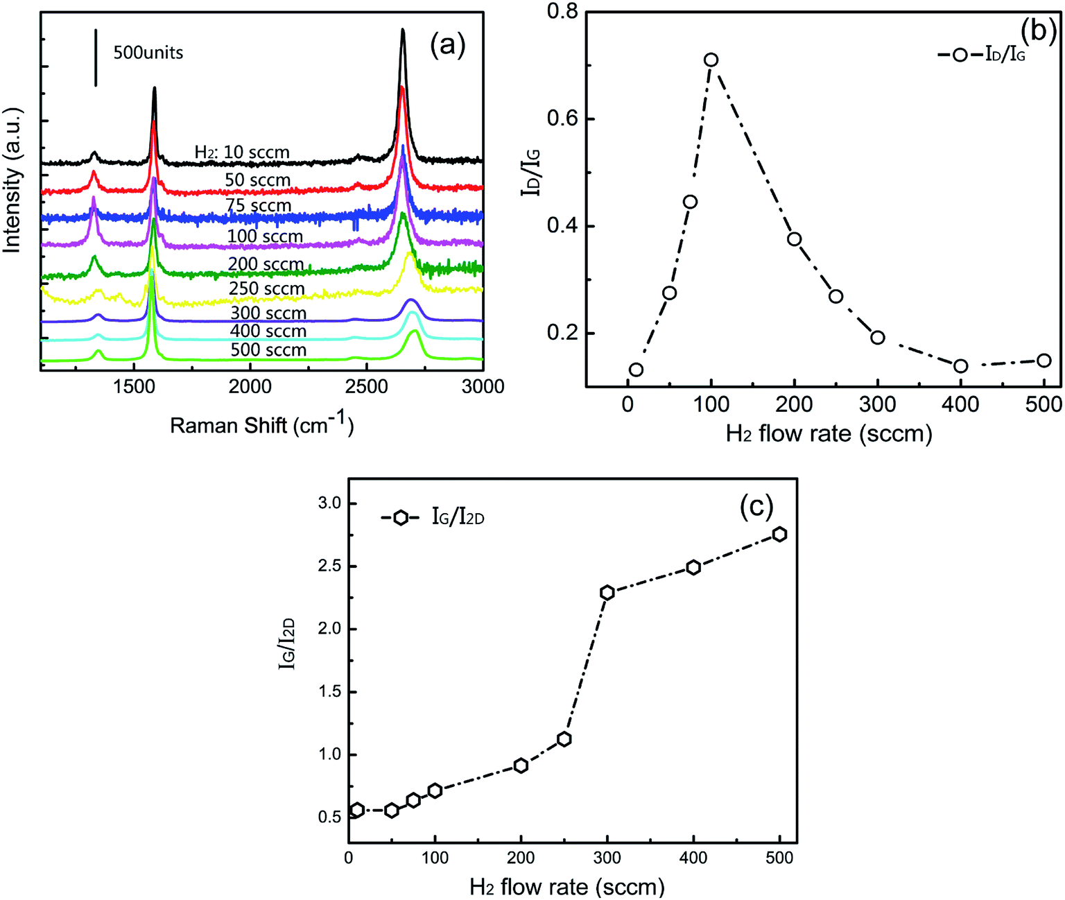 | ||
| Fig. 1 (a) Raman spectra of graphene grown at different flow rates of H2. (b) ID/IG ratio and (c) IG/I2D of graphene grown at different flow rates of H2. | ||
Fig. 2a–c show the C 1s XPS spectra for the samples G10, G100, and G200 on copper. These three C 1s XPS spectra are similar, and the C 1s of graphene is fitted by four peaks, which include four kinds of carbon-containing functional groups: C![[double bond, length as m-dash]](https://www.rsc.org/images/entities/char_e001.gif) C, C–C, C–H, and C–O. CC bonds and C–C bonds come from the structure of graphene, and C–H bonds in graphene surface comes from the hydrogen etching process. In an argon protected environment, oxygen may have originated from oxides, such as CuO and Cu2O, at the copper surface. During the reaction, these oxides are reduced into oxygen by hydrogen. Simultaneously, graphene is etched by the released oxygen, and then, the C–O bonds are generated in graphene in this process. It was observed that the percentage of C–H bonds was much less than that of C–O bonds in each sample, indicating that C–H would not obviously affect the distribution of the deposited Ag NPs. Fig. 2d shows that the percentage for C–O bonds increased when the flow rate of hydrogen was increased from 10 to 100 sccm and then decreased when more hydrogen was introduced. Graphene grain sizes and grain boundaries would saturate when the flow rate of hydrogen is increased to 100 sccm. Functional groups, such as C–O bonds, are mainly generated at grain boundaries.36 Thus, the amount of C–O bonds would change at the air–graphene grain boundaries, which are limited by the flow rate of hydrogen. It is known that C–O is electronegative and it tends to absorb the electropositive Ag atoms or clusters. This suggests that the electronegative C–O in graphene would promote the formation of Ag NPs and affect the distribution and morphology of the Ag NPs. Thus, it is necessary to investigate the relationship between the percentage of C–O and the formation of Ag NPs.
C, C–C, C–H, and C–O. CC bonds and C–C bonds come from the structure of graphene, and C–H bonds in graphene surface comes from the hydrogen etching process. In an argon protected environment, oxygen may have originated from oxides, such as CuO and Cu2O, at the copper surface. During the reaction, these oxides are reduced into oxygen by hydrogen. Simultaneously, graphene is etched by the released oxygen, and then, the C–O bonds are generated in graphene in this process. It was observed that the percentage of C–H bonds was much less than that of C–O bonds in each sample, indicating that C–H would not obviously affect the distribution of the deposited Ag NPs. Fig. 2d shows that the percentage for C–O bonds increased when the flow rate of hydrogen was increased from 10 to 100 sccm and then decreased when more hydrogen was introduced. Graphene grain sizes and grain boundaries would saturate when the flow rate of hydrogen is increased to 100 sccm. Functional groups, such as C–O bonds, are mainly generated at grain boundaries.36 Thus, the amount of C–O bonds would change at the air–graphene grain boundaries, which are limited by the flow rate of hydrogen. It is known that C–O is electronegative and it tends to absorb the electropositive Ag atoms or clusters. This suggests that the electronegative C–O in graphene would promote the formation of Ag NPs and affect the distribution and morphology of the Ag NPs. Thus, it is necessary to investigate the relationship between the percentage of C–O and the formation of Ag NPs.
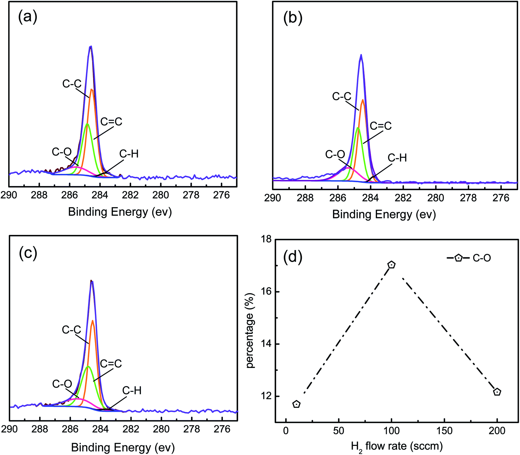 | ||
| Fig. 2 C 1s XPS spectra for samples of (a) G10, (b) G100, and (c) G200. (d) The percentage of C–O bonds for graphene. | ||
3.2. The distribution and morphology for the Ag NPs on graphene
As shown in Fig. 3a–g (the SEM images), Ag NPs were sputtered on graphene substrates with the same sputtering time. It was observed that the sizes and distances amongst Ag NPs are relatively uniform, but different in each sample. The sizes of Ag NPs become larger when the flow rate of hydrogen is increased from 10 to 100 sccm. The sizes of Ag NPs for the G100-Ag are larger than those of the rest of the samples, and these become more larger when the hydrogen flux exceeds 150 sccm. The heights of Ag NPs on G100 were detected by AFM, which ranged from 2 to 10 nm. However, the distances between adjacent Ag NPs become smaller with the flow rate of hydrogen, which ranges from 10 to 100 nm, and these become larger when the hydrogen flux exceeds 100 sccm. It was indicated that the average sizes for Ag NPs in the sample G100 were largest, but the distances were smallest. It is well known that the distance of less than 10 nm between adjacent particles is beneficial for forming hot spots for SERS. Fig. 3h shows the percentage of distances of less than 10 nm between Ag NPs calculated from the corresponding SEM images for the samples G10-Ag, G50-Ag, G100-Ag, G150-Ag, G200-Ag, G250-Ag, and G300-Ag. Every SEM image was averagely divided to 250 cells by the 50 × 50 grid. Inter-particle distance is defined as the smallest distance between the two particles in a cell. It increases with the flow rate of hydrogen ranging from 10 to 100 sccm and decreases with further increase in the flow rate of hydrogen. The percentage of G100-Ag reaches a maximum value because it contains much more electronegative C–O bonds to absorb Ag atoms or clusters to generate higher growth core density. These growth cores grow up and coalesce with each other to form irregular island shapes, which would contribute to narrowing the distances between Ag NPs to form hot spots, pointed out by the arrows in Fig. 3c. The percentage of C–O bonds sharply decreases when the flow rate of hydrogen exceeds 100 sccm. Most Ag atoms or clusters independently grow into big NPs because of the less active sites density, which is affected by the C–O bonds. It was considered that the maximum amount of hot spots would be generated on the sample G100-Ag, which would give the strongest SERS single.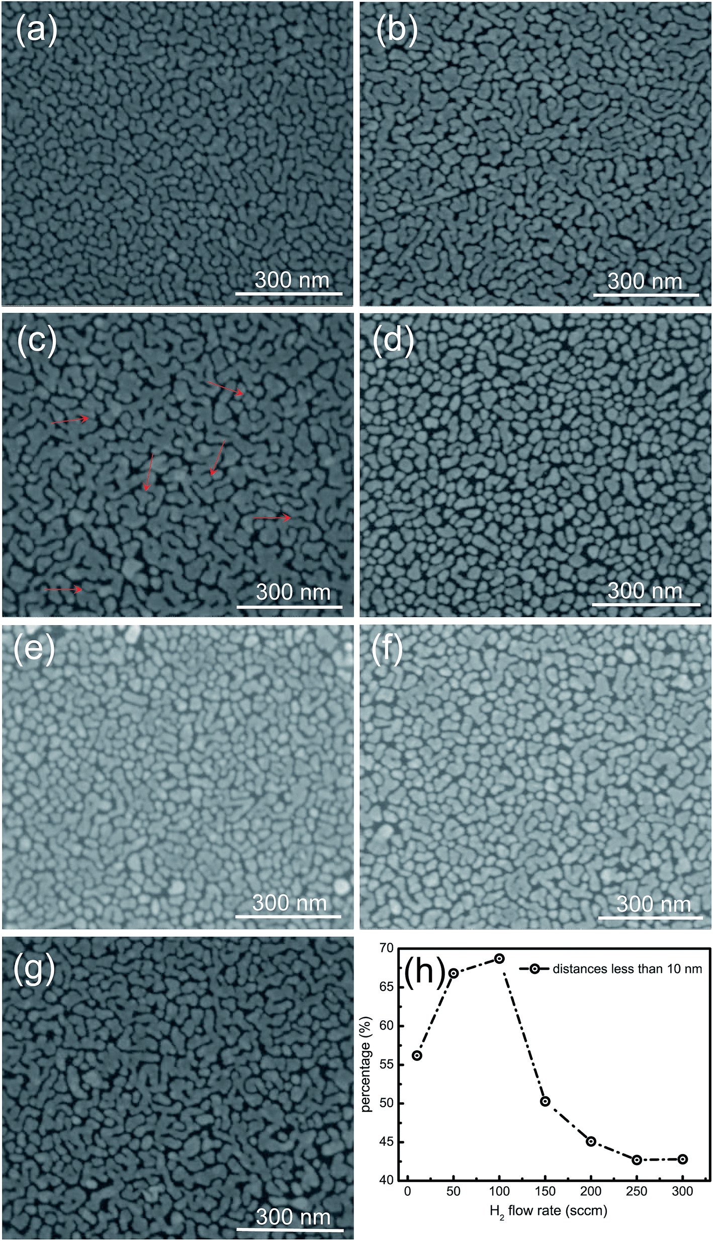 | ||
| Fig. 3 (a–g) SEM images for Ag NPs on the samples of G10, G50, G100, G150, G200, G250 and G300. (h) The percentage of distances between adjacent NPs less than 10 nm calculated from the corresponding SEM images. | ||
3.3. Raman spectra for G100 and G100-Ag
Fig. 4 shows the Raman spectra of G100 and G100-Ag (formed by the deposition of Ag on G100 for 90 s). It is shown that the sample G100 owns three graphene characteristic Raman bands: D, G, and 2D bands. By contrast, the sample G100-Ag owns not only the enhanced three Raman bands, but also the D′ band and another D + D′ band. According to the research reported by Kalbac et al.,41 the Raman signal of graphene is enhanced by energy transfer from surface plasmon resonance excited between Ag NPs. In addition, the doping of Ag NPs would induce the artificial defects in graphene, which result in the emergence of the D′ band and the enhancement of the D band.42 The D + D′ band is due to two-phonon defect-assisted process.43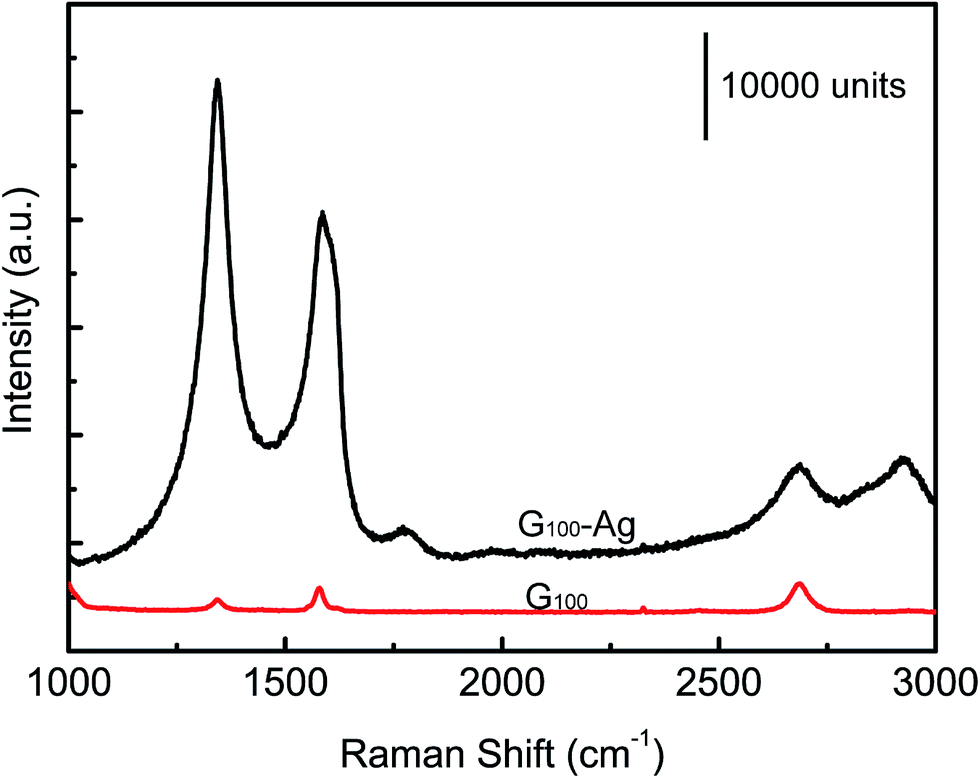 | ||
| Fig. 4 Raman spectra for G100 and G100-Ag. | ||
3.4. SERS spectra of R6G on Ag/graphene composites
Fig. 5 shows that Raman spectra of R6G molecules (10−5 M) on the graphene substrate of the sample G10 with different characteristic Ag NPs, prepared by sputtering at different sputtering times ranging from 15 to 120 s. It can be observed that Raman intensity shows an increase when the sputtering time is increased from 15 to 90 s. However, the Raman intensity sharply decreases on the prolonging sputtering time. It is anticipated that the sizes of Ag NPs are small and the distances of Ag NPs are too large at shorter sputtering time, whereas the Ag NPs would be converted to continuous films when the sputtering time is very long. It is obvious that the Raman intensity shows a decrease when the sputtering time is either too short or too long. The Ag NPs prepared by sputtering for 90 s on uniform graphene show the strongest SERS signal.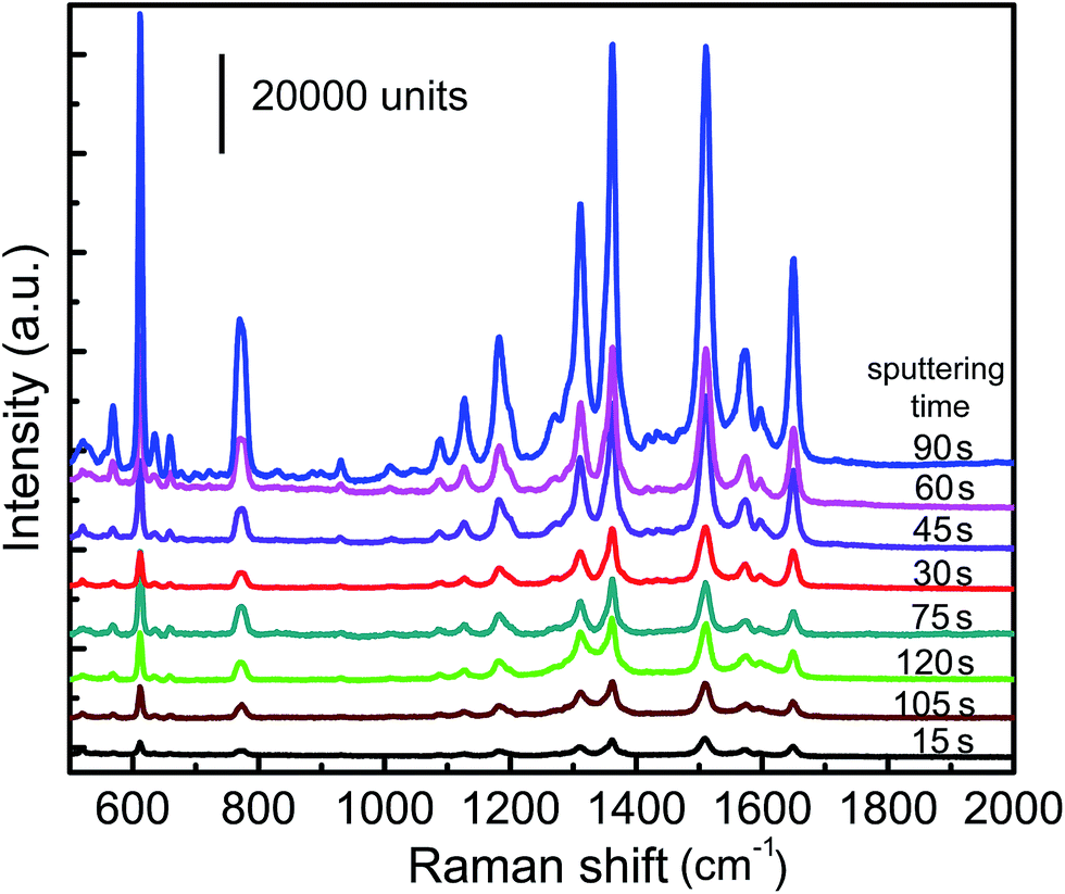 | ||
| Fig. 5 Raman spectra of R6G molecules (10−5 M) on graphene (G10) with Ag NPs prepared at different sputtering time. | ||
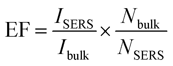
Ag NPs were homogeneously sputtered on graphene sheets for an optimal depositing time of 90 s. Fig. 6a shows the SERS spectra of R6G for different Ag/graphene substrates including G10-Ag, G50-Ag, G100-Ag, G150-Ag, G250-Ag, and G300-Ag. The positions of the R6G characteristic peaks 1130 cm−1, 1190 cm−1, 1360 cm−1, 1509 cm−1, 1575 cm−1, and 1650 cm−1 are generally in agreement with the previously reported measurement results.24,44 Amongst these samples, the sample G100-Ag shows the strongest Raman intensity and the Raman intensity of sample G250-Ag is the weakest compared with that of the other samples. The Raman intensity of G100-Ag is almost 0.5 × 10³ times stronger than that of the sample G250-Ag. In general, SERS results from a combination of the EM and the CM. The EM plays a main role for SERS and it is originated from the morphology of the Ag NPs. The sample G100 contains much more C–O bonds, which contribute to controlling the distribution of the Ag NPs covered on it. The percentage for distances less than 10 nm for the sample G100-Ag reaches a maximum value, and it would develop a maximum number of hot spots for SERS. The SERS EF change with the flow rate of hydrogen is shown in Fig. 6b. SERS EF is used to estimate the Raman enhancement effect amongst each sample. The SERS EF is calculated by the following formula:45
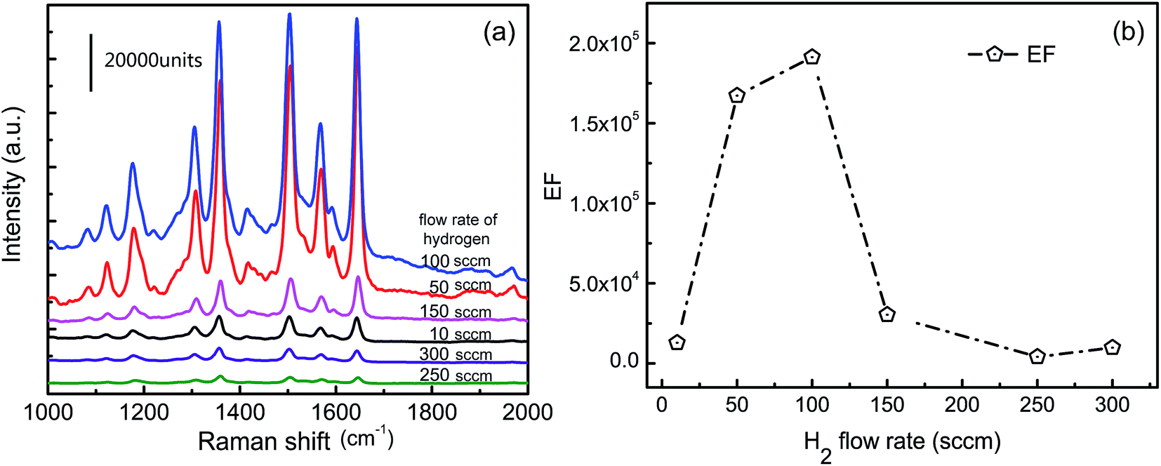 | ||
| Fig. 6 (a) SERS spectra of 10−7 M R6G for various samples: G10-Ag (90 s), G50-Ag (90 s), G100-Ag (90 s), G150-Ag (90 s), G250-Ag (90 s), and G300-Ag (90 s). (b) The SERS enhancement factor (EF). | ||
4. Conclusion
Graphene with different amounts of defects and layers was obtained by controlling the flow rate of hydrogen during the reacting process. The Ag NPs covered on the prepared graphene formed irregular island shapes, affected by the defects, which mainly consisted of C–O bonds in graphene. It was considered that the C–O bonds in graphene have the ability to provide active sites to absorb Ag atoms or clusters to create growth cores for Ag NPS, which would be developed to form hot spots for SERS. The SERS EF, the percentage of C–O bonds, and the percentages of distances of less than 10 nm between adjacent Ag NPs have the similar variation trend. The EF of G100-Ag shows the maximum reaching 105, which is almost 0.5 × 10³ times stronger than that of the sample G250-Ag having the weakest effect of SERS.Acknowledgements
This work was supported by the National Natural Science Foundation of China (No. 51661145025, 11274055).References
- M. G. Albrecht and J. A. Creighton, J. Am. Chem. Soc., 1977, 99, 5215–5217 CrossRef CAS.
- D. L. Jeanmaire and R. P. Van Duyne, J. Electroanal. Chem. Interfacial Electrochem., 1977, 84, 1–20 CrossRef CAS.
- G. L. Liu, Y. Lu, J. Kim, J. C. Doll and L. P. Lee, Adv. Mater., 2005, 17, 2683–2688 CrossRef CAS.
- J. J. Baumberg, T. A. Kelf, Y. Sugawara, S. Cintra, M. E. Abdelsalam, P. N. Bartlett and A. E. Russell, Nano Lett., 2005, 5, 2262–2273 CrossRef CAS PubMed.
- J. F. Li, Y. F. Huang, Y. Ding, Z. L. Yang, S. B. Li, X. S. Zhou, F. R. Fan, W. Zhang, Z. Y. Zhou, D. Y. Wu, B. Ren, Z. L. Wang and Z. Q. Tian, Nature, 2010, 464, 392 CrossRef CAS PubMed.
- D.-K. Lim, K.-S. Jeon, H. M. Kim, J.-M. Nam and Y. D. Suh, Nat. Mater., 2010, 9, 60 CrossRef CAS PubMed.
- M. Fleischmann, P. J. Hendra and A. J. McQuillan, Chem. Phys. Lett., 1974, 26, 163–166 CrossRef CAS.
- A. Otto, I. Mrozek, H. Grabhorn and W. Akemann, J. Phys.: Condens. Matter, 1992, 4, 1143 CrossRef CAS.
- G. C. Schatz, M. A. Young and R. P. Duyne, Top. Appl. Phys., 2006, 103, 19–45 CrossRef CAS.
- E. C. L. Ru and P. G. Etchegoin, Principles of Surface-Enhanced Raman Spectroscopy and Related Plasmonic Effect, 2009, vol. 47, pp. 415–464 Search PubMed.
- M. Udagawa, C. C. Chou, J. C. Hemminger and S. Ushioda, Phys. Rev. B: Condens. Matter Mater. Phys., 1981, 23, 6843–6846 CrossRef CAS.
- X. D. Jiang and A. Campion, Chem. Phys. Lett., 1987, 140, 95–100 CrossRef CAS.
- M. Fan, G. F. S. Andrade and A. G. Brolo, Anal. Chim. Acta, 2011, 693, 7–25 CrossRef CAS PubMed.
- Y. Han, R. Lupitskyy, T. M. Chou, C. M. Stafford, H. Du and S. Sukhishvili, Anal. Chem., 2011, 83, 5873–5880 CrossRef CAS PubMed.
- S. Malynych and G. Chumanov, J. Am. Chem. Soc., 2003, 125, 2896–2898 CrossRef CAS PubMed.
- N. M. Kha, C. H. Chen and W. N. Su, Phys. Chem. Chem. Phys., 2015, 17, 21226–21235 RSC.
- W. Xu, X. Ling, J. Xiao, M. S. Dresselhaus, J. Kong, H. Xu, Z. Liu and J. Zhang, Proc. Natl. Acad. Sci. U. S. A., 2012, 109, 9281–9286 CrossRef CAS PubMed.
- F. Bonaccorso, Z. Sun, T. Hasan and A. C. Ferrari, Nat. Photonics, 2010, 4, 611–622 CrossRef CAS.
- A. H. C. Neto, F. Guinea, N. M. R. Peres, K. S. Novoselov and A. K. Geim, Rev. Mod. Phys., 2009, 81, 109–162 CrossRef.
- C. G. Lee, X. D. Wei, J. W. Kysar and J. Hone, Science, 2008, 321, 385–388 CrossRef CAS PubMed.
- G. Lu, H. Li, C. Liusman, Z. Yin, S. Wu and H. Zhang, Chem. Sci., 2011, 2, 1817–1821 RSC.
- Y. Wang, Z. Ni, H. Hu, Y. Hao, C. P. Wong, T. Yu, J. T. L. Thong and Z. X. Shen, Appl. Phys. Lett., 2010, 97, 163111 CrossRef.
- M. Losurdo, I. Bergmair, B. Dastmalchi, T.-H. Kim, M. M. Giangregroio, W. Jiao, G. V. Bianco, A. S. Brown, K. Hingerl and G. Bruno, Adv. Funct. Mater., 2014, 24, 1864–1878 CrossRef CAS.
- Y. Liu, Y. Hu and J. Zhang, J. Phys. Chem. C, 2014, 118, 8993–8998 CAS.
- X. Li, W. C. H. Choy and X. Ren, Adv. Funct. Mater., 2014, 24, 3114–3122 CrossRef CAS.
- J. Leem, M. C. Wang and P. Kang, Nano Lett., 2015, 15 Search PubMed.
- X. Fu, L. Pan and S. Li, Appl. Surf. Sci., 2015, 363, 412–420 CrossRef.
- X. Wang, G. Meng and C. Zhu, Adv. Funct. Mater., 2013, 23, 5771–5777 CrossRef CAS.
- C. Mattevi, H. Kim and M. Chhowalla, J. Mater. Chem., 2011, 21, 3324–3334 RSC.
- X. Li, Science, 2009, 324, 1312–1314 CrossRef CAS PubMed.
- L. Xuesong, C. Weiwei and A. Jinho, Science, 2009, 324, 1312–1314 CrossRef PubMed.
- X. Li, Y. Zhu and W. Cai, Nano Lett., 2009, 9, 4359–4363 CrossRef CAS PubMed.
- A. Umair and H. Raza, Nanoscale Res. Lett., 2012, 7, 1–5 CrossRef PubMed.
- A. Das, B. Chakraborty and A. K. Sood, Bull. Mater. Sci., 2007, 31, 579–584 CrossRef.
- S. Hussain, M. W. Iqbal and J. Park, et al., Physical and electrical properties of graphene grown under different hydrogen flow in low pressure chemical vapor deposition, Nanoscale Res. Lett., 2014, 9(1), 546 CrossRef PubMed.
- M. Kalbac, O. Frank and L. Kavan, The control of graphene double-layer formation in copper-catalyzed chemical vapor deposition, Carbon, 2012, 50(10), 3682–3687 CrossRef CAS.
- I. Vlassiouk, M. Regmi and P. Fulvio, et al., Role of hydrogen in chemical vapor deposition growth of large single-crystal graphene, ACS Nano, 2011, 5(7), 6069 CrossRef CAS PubMed.
- J. An, E. Voelkl and W. S. Ji, et al., Domain (Grain) Boundaries and Evidence of “Twinlike” Structures in Chemically Vapor Deposited Grown Graphene, ACS Nano, 2011, 5(4), 2433–2439 CrossRef CAS PubMed.
- J. H. Jang, J. C. Yoon and P. Thiyagarajan, RSC Adv., 2015, 5, 62772–62777 RSC.
- Y. K. Yang, C. E. He and W. J. He, J. Nanopart. Res., 2011, 13, 1–11 CrossRef.
- M. Kalbac, V. Vales and J. Vejpravova, The effect of a thin gold layer on graphene: A Raman spectroscopy study, RSC Adv., 2014, 4(105), 60929–60935 RSC.
- H. Liu, S. Ryu and Z. Chen, et al., Photochemical Reactivity of Graphene, J. Am. Chem. Soc., 2009, 131(47), 17099–17101 CrossRef CAS PubMed.
- A. C. Ferrari and D. M. Basko, Raman spectroscopy as a versatile tool for studying the properties of graphene, Nat. Nanotechnol., 2013, 8(4), 235 CrossRef CAS PubMed.
- E. S. Thrall, A. C. Crowther and Y. Zhonghua, Nano Lett., 2012, 12, 1571–1577 CrossRef CAS PubMed.
- W. B. Cai, B. Ren and X. Q. Li, Surf. Sci., 1998, 406, 9–22 CrossRef CAS.
| This journal is © The Royal Society of Chemistry 2017 |