
 Open Access Article
 This Open Access Article is licensed under a
 Creative Commons Attribution 3.0 Unported Licence
Metal–insulator–semiconductor field-effect transistors (MISFETs) using p-type SnS and nanometer-thick Al2S3 layers†
Devika Mudusu‡
ab,
Koteeswara Reddy Nandanapalli‡ *cd,
Sreekantha Reddy Dugasani‡d,
Ramesh Karuppannane,
Gunasekhar Kothakota Ramakrishna Reddyf,
Raja Gopal Erode Subramaniane and
Sung Ha Park*d
*cd,
Sreekantha Reddy Dugasani‡d,
Ramesh Karuppannane,
Gunasekhar Kothakota Ramakrishna Reddyf,
Raja Gopal Erode Subramaniane and
Sung Ha Park*d
aDepartment of Aerospace Engineering, Indian Institute of Science, Bangalore 560012, India
bSchool of Advanced Materials Science & Engineering, Sungkyunkwan University, Suwon, Gyeonggi-do 16419, South Korea
cCenter for Nanoscience and Engineering, Indian Institute of Science, Bangalore 560012, India. E-mail: dr_nkreddy@rediffmail.com
dDepartment of Physics, Sungkyunkwan Advanced Institute of Nanotechnology (SAINT), Sungkyunkwan University, Suwon 16419, South Korea. E-mail: sunghapark@skku.edu
eDepartment of Physics, Indian Institute of Science, Bangalore 560012, India
fDepartment of Instrumentation and Applied Physics, Indian Institute of Science, Bangalore 560012, India
First published on 16th February 2017
Abstract
Novel and cost-effective metal–insulator semiconductor field-effect transistor (MISFET) devices were fabricated using non-toxic tin mono sulfide (SnS) as the active layer sandwiched between aluminium and silver contacts with an unintentionally grown aluminium sulfide (Al2S3) interface layer. MISFET devices exhibit a high turn-on voltage of 5.13 V and excellent rectifying diode characteristics. These devices also show a high rectification factor of 1383 at a bias voltage of 6 V and series resistance of 3.4 MΩ, along with a very low leakage current of ∼10−9 A@−10 V. The overall results reveal that it could be possible to fabricate cost-effective and non-toxic MISFET devices by using SnS as an active layer for various power-electronic applications.
Introduction
In recent years, tin mono sulfide (SnS) semiconductor material has received considerable attention as an absorber material particularly for photovoltaic applications.1–3 In general, SnS thin films exhibit a direct optical band gap of 1.35 eV and high absorption coefficient of ∼105 cm−1.4–6 Thin films of SnS have been prepared using various chemical and physical methods,7–20 and their electrical properties are easily tailored by doping appropriate dopants.21–24 Orthorhombic structured SnS exhibits stable structural and optical properties up to a maximum temperature of 600 °C.18,25 Compared to other efficient absorber materials, the toxicity and cost of SnS are low,26 and the achievable maximum light conversion efficiency with SnS is about 25%.27Although the studies on SnS thin films based devices are still at a preliminary level, a wide range of interesting and important applications have been made, including in photovoltaics, optoelectronics, chemical sensors, solid-state batteries, and holography register systems etc. Considering the scope of the present paper, the literature review was limited to SnS thin film based photovoltaic (PV) devices. Noguchi et al. observed 0.29% light conversion efficiency from devices fabricated with the configuration of ITO/n-CdS/p-SnS/Ag.28 Masaya group observed the photovoltaic (PV) conversion efficiency of 0.22% from CdS/SnS cells and 0.71% from Cd0.87Zn0.13S/SnS cells.29 Solar cell devices fabricated by evaporation of CdS and SnS materials onto ITO substrate30 exhibited a low efficiency of 0.08%, whereas the PV devices developed with SnS/ZnO exhibited considerable efficiency of 1.29%.31 Further, the devices developed using nanocrystalline SnS and TiO2 layers showed a light conversion efficiency of 0.1%.32 On the other hand, the PV devices fabricated with lead sulfide (PbS) and SnS films exhibited a power conversion efficiency of 0.27%.33 More recently, SnS solar cell devices fabricated using Zn1−2xMgxO as the buffer layer showed the light conversion efficiency of about 2.1%.34 However, a noticeable problem in the development of efficient SnS based PV devices is the selection of a suitable n-type material, which greatly hinders the potential applications of SnS. Many scientists are thus focusing on the SnS based Schottky as well as metal–insulator–semiconductor (MIS) devices that exclude the requirement of n-type layers.
On the other hand, Schottky diodes, developed with different conventional semiconductor materials (Si, GaAs, GaN, InP and SiC)35–39 play a crucial role as detectors, rectifiers, light converters, switches and couplers. Although these devices have better performance and excellent durability, today researchers are looking for a new class of materials due to high fabrication cost and toxicity of the existing materials. As stated above, SnS is one of the cost-effective and nontoxic materials and can be synthesized using different low-cost techniques. Thus, it facilitates the production of low-cost and toxic-free Schottky devices. However, up to now, only minimal work has been carried out on the development of SnS based Schottky diodes.40–43 For example, the Safak group have explored the Schottky device properties and noticed an increase in barrier height (0.47–0.52 eV) of Ag/SnS devices with the increase of temperature from room temperature (RT) to 100 °C.44 Further, while decreasing temperature from RT to low, a gradual decrease in barrier height and increase in series resistance have been observed.43,45 More recently, Das and colleagues as well as Mathews have studied the electrical behavior of SnS films with Al contacts. Here, Das and colleagues observed nearly ohmic characteristics from the Al/SnS/In structures even for annealed SnS films,41 whereas Mathews observed Schottky barrier properties from ITO/SnS/Al structures.40 On the other hand, our group noticed typical properties such as crystallinity, preferential growth, and optical quality from SnS films deposited on latticed matched Al substrates.46 These interesting features of SnS films motivated us to investigate the electrical properties of SnS films by depositing them over Al coated substrates.
In this study, we fabricated p-type SnS nanocrystals based Schottky devices with the configuration of Al/SnS/Ag, and realized MISFET device characteristics due to the unintentionally grown Al2S3 layer between Al and SnS as the interface layer. The morphology, crystal structure and quality of SnS structures deposited on Al coated glass substrates were studied and compared with the properties of SnS structures deposited on bare glass substrate. The performance of MISFET devices was investigated at room temperature. The as-grown devices exhibited high turn-on voltage of 5.13 V and very low leakage current (10−9 A@−10 V), which are highly desirable parameters for different applications including high power devices, microwave devices and optoelectronic devices.
Experimental procedure
SnS nanostructures based devices with an Al/(Al2S3)/SnS/Ag sandwich configuration were fabricated on glass substrates using thermal evaporation technique and the charge transport characteristics were studied with the probe-station as described below.Fabrication of devices
As shown in the schematic diagram in Fig. 1, initially a thin layer (∼100 nm) of high pure aluminium (Al with 4N purity) was deposited on cleaned glass substrates (Step-I). The deposition was carried out in a thermal evaporation system, without any applied heating, under a vacuum of ∼10−6 Torr. The rate of deposition was maintained at 2 nm s−1. SnS nanostructures were grown with a deposition rate of 0.2 nm s−1 and thickness of 250 nm at a substrate temperature of 350 °C on bare glass substrates (used for comparison) and Al coated glass substrates (Step-II).47 In the case of glass/Al substrates, a piece of glass was used as a mask to protect the small portion of the Al layer from SnS deposition. Without breaking the vacuum, the structures were kept under the same condition for 10 min and cooled down to room temperature. Then, point-shaped silver (Ag with 4N purity) contacts were deposited at RT on glass/Al/SnS structures with a gap of 5 mm (thickness ∼100 nm) by using a mask under the same vacuum condition (Step-III).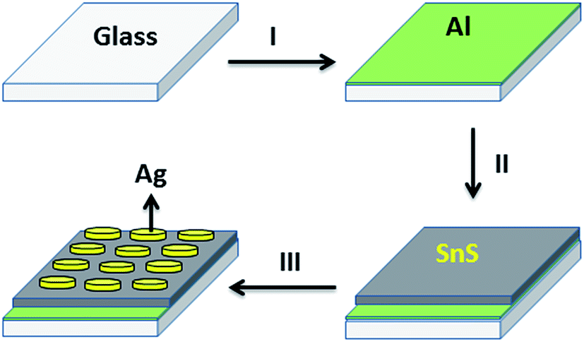 | ||
| Fig. 1 Schematic representation of fabrication of Al/(Al2S3)/SnS/Ag MISFET device. | ||
Characterization
The surface morphology and chemical composition of SnS structures grown on both the substrates were analyzed using field emission scanning electron microscopy (FESEM, ZEISS ULTRA 55, Gemini), noncontact optical profilometer (TalySurf CCI MP) and energy dispersive X-ray spectroscopy (EDS, Oxford Instruments) attached with FESEM. The crystal structure and phase purity of SnS structures were studied using an X-ray diffractometer (XRD, Phillip's XPERT PRO, PANalytical B.V., The Netherlands) with Cu Kα1 radiation (λ = 0.1541 nm) and micro Raman spectroscopy (Lab RAM HR (HORIBA JOBINYUON)). The electrical resistance of SnS nanostructures grown on Al coated glass substrates, and the carrier transport properties of the Al/(Al2S3)/SnS/Ag devices were estimated by measuring the current–voltage (I–V) characteristics with a probe station attached to a semiconductor parameter analyzer (Agilent Device Analyzer B1500A).Results and discussion
The SnS structures deposited on Al coated glass substrates appear to be light-brown in color, whereas the structures on bare glass appear to be dark-brown in color. The physical properties (surface morphology, composition, crystal structure and optical vibrational modes) of SnS structures deposited on Al coated glass substrates are described here by comparing with the data obtained from the structures deposited on bare glass substrates.Basic properties
FESEM studies (Fig. 2) show that the surface features of the SnS structures developed on the two different substrates are almost similar. However, the surface of the SnS structures on glass is comparatively rougher than that of the structures grown on Al layers (see ESI-1a and b†), which is probably attributed to the variation of the adatom mobility of the evaporated atoms on different surfaces.48 Compared to earlier results,47–49 the present SnS structures consist of a unique surface morphology, which is mainly attributed to the post-annealing of structures. On the other hand, the cross-section FESEM image (Fig. 2c) shows that SnS structures consist of nanocrystalline crystals, which have almost orthorhombic crystal shapes. These results are very close to those of our earlier reported work.47 EDS studies show that the SnS structures grown on both the substrates have an almost stoichiometric chemical composition (see ESI-2† for EDS spectra). However, the Sn to S atomic percentage ratio of SnS structures grown on Al coated and bare glass substrates is found to be 1.06 and 1.03, respectively. This reveals that comparatively, the SnS structures on the Al coated glass substrates consist of a slightly tin-rich (or sulfur deficient) chemical composition. | ||
| Fig. 2 FESEM images of SnS structures grown on (a) Al coated and (b) bare glass substrates, (c) cross-section FESEM image of SnS structures on Al coated glass substrates and (d) elemental composition of SnS structures grown on (top) Al coated and (bottom) bare glass substrates. | ||
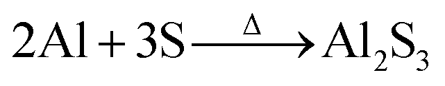
XRD profiles of SnS structures grown on Al coated and bare glass substrates are shown in Fig. 3, and all diffracted peaks are indexed with corresponding planes of SnS and Al. The profile of SnS structures grown on Al layers (Fig. 3b) shows three dominant peaks diffracted at 2θ = 32.03, 44.8 and 66.3°, which belong to SnS (040), SnS (141) and/or Al (200), and Al (220), respectively, since the calculated d-spacing values of these peaks exactly match the orthorhombic SnS and cubic Al (JCPDS: 39-0354 and 04-0787). The remaining weak diffraction peaks belong to SnS, implying that SnS crystallites on Al coated glass substrates are preferentially orientated along the 〈010〉 direction. Compared to the SnS structures grown on glass substrate (Fig. 3a), the intensity of the preferential peak of the SnS structures on the Al layer is higher and broader. To determine the reason for the broadness of the preferential peak, the elaborated XRD spectrum of SnS structures grown on Al layers was fitted with multi-peak Gaussian function. This reveals that the broad peak consists of an additional diffraction peak along with the SnS (040) peak at 2θ = 31.56° (ESI-2 and 3†), which probably belongs to aluminium sulfide (Al2S3).50 This Al2S3 might have formed as an interfacial layer at the time of the growth of the SnS structures on the Al coated glass substrate, which can be expressed by a chemical equation as:
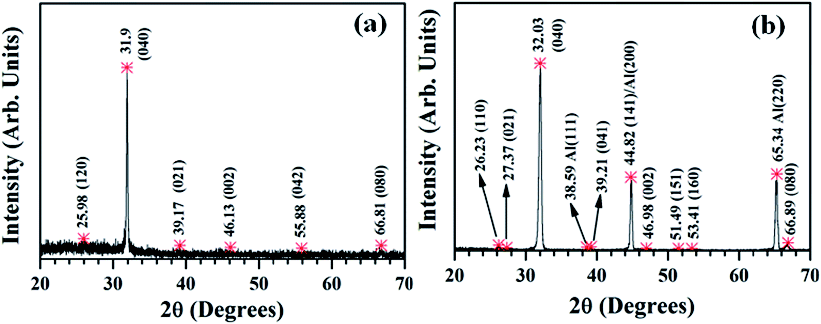 | ||
| Fig. 3 XRD profile of SnS structures grown on (a) bare and (b) Al coated glass substrates. | ||
Micro Raman spectroscopy studies (Fig. 4) show that the SnS structures grown on both substrates consist of four distinguishable Raman peaks at 94, 159, 185 and 217 cm−1. These peaks can be attributed to the first order single-phonon-oriented transverse or longitudinal optical (TO and LO) vibration modes, and are assigned to Ag(TO), B2g(LO), Ag(LO1) and Ag(LO2), respectively. However, the Raman peaks that observed at higher wavenumbers, i.e. 255 and 478 cm−1, belong to the Al3S3 phase.51,52 On the other hand, compared to the Raman spectrum of the SnS structures grown on glass substrates (Fig. 4a), the nanostructures grown on Al coated substrates consist of sharp lines and exhibit considerable shifts in positions, which can be attributed to surface smoothness and/or crystalline quality of the SnS structures.47,53 For example, Akgul et al. noticed sharp Raman peaks with low full width at half maximum (FWHM) values from highly crystalline copper oxide films,54 whereas the increase in sharpness of Raman peaks was noticed by Zgheib et al. while fabricating silicon carbide thin films over germanium modified substrates.55 Furthermore, these results are consistent with our earlier results of SnS structures grown with slow-rate of deposition over glass substrates at different temperatures.46
 | ||
| Fig. 4 Raman spectrum of SnS nanostructures deposited on (a) bare and (b) Al coated glass substrates. | ||
Therefore, the XRD and Raman studies along with chemical composition analyses clearly emphasized that Al2S3 was formed as an interfacial layer between the Al and SnS structures, which probably acts as an insulating layer between metal (Al) and semiconductor (SnS) structures.
Device characteristics
I–V plots measured between Ag–Ag and Ag–Al contacts are shown in Fig. 5. Measurements between Ag and Ag circular contacts show that these silver contacts have ohmic characteristics with SnS nanostructures grown on Al coated glass substrates (Fig. 5a). The resistivity of SnS columnar structures, from the linear slope of the I–V curve, is found to be 6.7 Ω cm. This value is very low compared to the electrical resistivity of SnS structures deposited on glass substrates.56 On the other hand, I–V measurements between Ag and Al contacts exhibit non-ideal and rectifying characteristics (Fig. 5b), which is discussed in detail at the end of the section using energy band diagram of the device. This noticeable rectification behavior of the device is probably attributed to the unintentionally formed insulating Al2S3 layer between the Al and SnS structures as the interfacial layer, since the Al contacts deposited on SnS films at the substrate temperature of 50 °C exhibited ohmic characteristics.57 | ||
| Fig. 5 Current–voltage plots of SnS nanocrystalline structures measured between (a) Ag and Ag contacts (inset shows a photograph of Ag contacts deposited on SnS structures over Al coated glass substrates) and (b) Al and Ag contacts. | ||
Under both bias conditions, the current flow through the devices, although the magnitudes differ, starts at above a certain bias voltage (±3.2 V), which can be clearly observed in Fig. 6. This typical voltage is treated as an interfacial barrier potential (VIB). Above VIB, the changes in current flow of the device in reverse-bias condition are marginal, whereas in forward-bias, they are significant. These devices exhibit a turn-on voltage of 5.13 V and high rectification factor of 1383 at a bias voltage of ±6 V (Fig. 6a) since the magnitude of current in the device at ±6 V is about 0.26 and 1.88 × 10⁻⁴ A, respectively.58 Further, the overall current flow through the device in forward-bias condition is significantly high, which is in the order of μA, whereas in reverse bias, it is in the order of nA. These results clearly reveal that the devices fabricated with the configuration of Al/(Al2S3)/SnS/Ag consist of MISFET device characteristics.
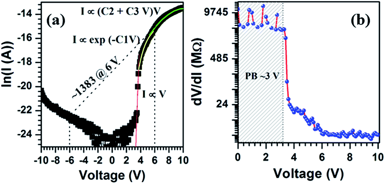 | ||
| Fig. 6 (a) ln(current) versus voltage plot measured in reverse and forward bias conditions (−10 to 10 V) and (b) dV/dI versus voltage plot measured only in forward bias condition (0–10 V) of Al/(Al2S3)/SnS/Ag structures. | ||
Variation in in situ series resistance (Rs) of the device (Rs = dV/dI) with the increase of forward-bias voltage (Fig. 6b) shows three distinguishable regions (<3.2, 3.2–6 and >6 V).59 As discussed in the literature, the device resistance at below 3.2 V is too high (∼109 Ω), which reflects an insulator capacitor characteristic, whereas at higher voltages, >6 V, the resistance of the device is nearly constant at 106 Ω, which is similar to a Schottky type capacitor. Under moderate bias voltages, the device behavior includes both the insulator and Schottky capacitor. Therefore, the presence of the Al2S3 layer as an interfacial barrier between the Al and SnS nanostructured layers (since Al2S3 is a wide band gap material,60 and most of the other parameters are not yet known) probably acts as an insulating layer and strongly influences the device properties.61
To understand the transport mechanism of charge carriers, the experimental data was fitted to the diode equation given below.40
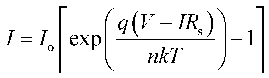
 , A is the effective area of the diode, A* is the effective Richardson constant (25 A cm−2 K−2 for SnS since the effective mass of the electron is about 0.22mo), T is the absolute temperature, q is the charge of electron, ϕb is the barrier height, k is the Boltzmann constant (1.38 × 10⁻²³ J K−1)], V is the applied bias voltage, Rs is the series resistance and n is the ideality factor of the diode. The nature of the ln(I) versus voltage curve of the device in reverse and forward bias conditions is shown in Fig. 6a. It is clearly revealed that at above 3.2 V, the current flow through the device follows three different mechanisms. Initially, it increases sharply with the increase of forward bias voltage up to 4 V and follows simple I ∝ V relation. This implies that between 3 and 4 V, the device consists of a thermionic emission or field emission transport mechanism (ohmic conduction). Based on the above equation, the device parameters ideality factor (n) and saturation current (Io) of the device are found to be 2.35 and 10−35 A, respectively. Further, the barrier height ϕb of the device is found to be 2.37 V.43 Compared to previous results on SnS Schottky diodes, the ideality factor and barrier height of the present device are too high, which can be attributed to the presence of the Al2S3 interfacial layer.62 At moderate voltages (4–6 V), the current flow through the device varied exponentially with the increase of bias voltage (i.e. I ∝ exp(−C1V), where C1 = 0.94). This implies that the carrier transport mechanism gradually changes with an increase of bias-voltage from thermionic emission to recombination-tunneling. On the other hand, at higher voltages, >6 V, the current flow through the device is strongly determined by the thermionic emission as well as by the space-charge limited current transport mechanism, since I ∝ (C2V + C3V2), where C2 and C3 are 1.77 and −0.09, respectively. Here, the observed exponential constant under recombination-tunneling characteristics (i.e. C1 = 0.94) is low and thus the injection of carriers, and thereby recombination of trap states in the device is moderate. At higher voltages, the negative sign of C3 constant (−0.09) indicates that the influence of space-charge carriers on the current flow of the device gradually increases with increase of bias voltage. These results are very similar to those of the MISFET devices fabricated with GaAs structures.59
Carrier transport mechanism
The MISFET device behavior with bias voltage can be understood with the help of the schematic energy band diagram of the Al/Al2S3/SnS/Ag structure, as shown in Fig. 7 along with individual elements. When the applied bias voltage at Al is negative, the electrons move towards SnS and the holes move in the opposite direction. Thus, the recombination of the carriers increases at around the Al2S3 interface and thereby increases the barrier height (eVbi), which creates immobilized cations. Therefore, the current flow through the device is mainly attributed to diffusion with the recombination of a few carriers. Consequently, the current flow through the device in reverse bias conditions is significantly low.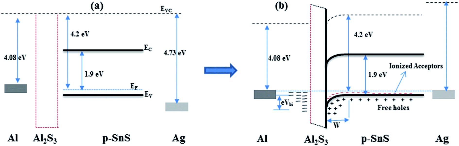 | ||
| Fig. 7 Schematic energy band diagram of (a) Al, Al2S3, p-SnS and Ag; and (b) Al/(Al2S3)/p-SnS/Ag structure. | ||
When the applied bias voltage at Al is positive, both carriers (i.e. holes and electrons) move in the opposite direction and thus, the barrier height of the device decreases with the increase of bias voltage. At moderate voltage, the successful recombination of electrons with holes dominates the device current flow, as noticed above. Thus, the device fabricated with Al/SnS/Ag with an unintentionally grown Al2S3 interface layer works as a MISFET. However, to understand the device properties of Al/(Al2S3)/SnS/Ag structures in detail, further studies need to be carried out such as capacitance–voltage, interface analysis and temperature dependent I–V properties of the device. Further, a detailed investigation is needed on Al2S3 structures.
Conclusions
SnS nanostructures based Schottky devices were fabricated using Al and Ag contacts and the electrical transport characteristics were investigated at room temperature. The as-grown SnS structures on Al coated glass substrates consist of stoichiometric chemical composition and exhibited an electrical resistivity of 6.7 Ω cm. Al/SnS/Ag devices exhibited metal–insulator–semiconductor FET characteristics with a high turn-on voltage of +5.13 V due to the presence of the unintentionally grown Al2S3 layer as the interfacial layer between Al and SnS. The leakage current under reverse bias-voltage is extremely low, ∼10−9 A at 10 V, and the rectification factor of the device at a bias voltage of 6 V is found to be 1383. These overall outcomes strongly emphasize that SnS based MISFET devices could have applications in different fields including power, microwave and optoelectronic devices where high turn-on voltage and high breakdown voltages are prerequisites.Note added after first publication
This article replaces the version published on February 13, 2017, which did not correctly attribute the author contributions.Acknowledgements
NKR wishes to acknowledge the CSIR for the sanction of the Senior Research Association under the scheme of the Scientist's Pool (No. 13(8525-A) 2011-Pool). MD wishes to acknowledge university grant commission (UGC), India for the sanction of Dr D. S. Kothari's Postdoctoral fellowship (No. F.4-2/2006(BSR)/13-703/2012(BSR)). NKR and SHP wish to acknowledge the partial support of Korean Federation of Science and Technology Societies grant funded by the Korean government (Ministry of Science, ICT and Future Planning) through the Brain Pool Fellowship and National Research Foundation of Korea (2014R1A2A1A11053213).References
- G. A. Tritsaris, B. D. Malone and E. Kaxiras, J. Appl. Phys., 2013, 113, 233507 CrossRef.
- M. Steichen, R. Djemour, L. Gutay, J. Guillot, S. Siebentritt and P. J. Dale, J. Phys. Chem. C, 2013, 117, 4383–4393 CAS.
- R. W. Miles, O. E. Ogah, G. Zoppi and I. Forbes, Thin Solid Films, 2009, 517, 4702–4705 CrossRef CAS.
- M. Devika, K. T. R. Reddy, N. K. Reddy, K. Ramesh, R. Ganesan, E. S. R. Gopal and K. R. Gunasekhar, J. Appl. Phys., 2006, 100, 023518 CrossRef.
- K. T. R. Reddy, P. P. Reddy, R. Datta and R. W. Miles, Thin Solid Films, 2002, 403, 116–119 CrossRef.
- R. E. Banai, H. Lee, M. A. Motyka, R. Chandrasekharan, N. J. Podraza, J. R. S. Brownson and M. W. Horn, IEEE Journal of Photovoltaics, 2013, 3, 1084–1089 CrossRef.
- S. Y. Cheng and G. Conibeer, Thin Solid Films, 2011, 520, 837–841 CrossRef CAS.
- E. Guneri, F. Gode, C. Ulutas, F. Kirmizigul, G. Altindemir and C. Gumus, Chalcogenide Lett., 2010, 7, 685–694 CAS.
- E. Guneri, C. Ulutas, F. Kirmizigul, G. Altindemir, F. Gode and C. Gumus, Appl. Surf. Sci., 2010, 257, 1189–1195 CrossRef CAS.
- A. Tanusevski, Semicond. Sci. Technol., 2003, 18, 501–505 CrossRef CAS.
- L. K. Khel, S. Khan and M. I. Zaman, J. Chem. Soc. Pak., 2005, 27, 24–28 CAS.
- N. Sato, M. Ichimura, E. Arai and Y. Yamazaki, Sol. Energy Mater. Sol. Cells, 2005, 85, 153–165 CrossRef CAS.
- K. Takeuchi, M. Ichimura, E. Arai and Y. Yamazaki, Sol. Energy Mater. Sol. Cells, 2003, 75, 427–432 CrossRef CAS.
- K. Hartman, J. L. Johnson, M. I. Bertoni, D. Recht, M. J. Aziz, M. A. Scarpulla and T. Buonassisi, Thin Solid Films, 2011, 519, 7421–7424 CrossRef CAS.
- J. Henry, K. Mohanraj, S. Kannan, S. Barathan and G. Sivakumar, Eur. Phys. J.: Appl. Phys., 2013, 61, 10301 CrossRef.
- A. Tanusevski and D. Poelman, Sol. Energy Mater. Sol. Cells, 2003, 80, 297–303 CrossRef CAS.
- N. K. Reddy and K. T. R. Reddy, Thin Solid Films, 1998, 325, 4–6 CrossRef.
- N. K. Reddy, Y. B. Hahn, M. Devika, H. R. Sumana and K. R. Gunasekhar, J. Appl. Phys., 2007, 101, 093522 CrossRef.
- A. Sanchez-Juarez, A. Tiburcio-Silver and A. Ortiz, Thin Solid Films, 2005, 480, 452–456 CrossRef.
- N. Koteeswara Reddy, K. Ramesh, R. Ganesan, K. T. Ramakrishna Reddy, K. R. Gunasekhar and E. S. R. Gopal, Appl. Phys. A: Mater. Sci. Process., 2006, 83, 133–138 CrossRef CAS.
- K. S. Kumar, A. G. Manohari, S. Dhanapandian and T. Mahalingam, Mater. Lett., 2014, 131, 167–170 CrossRef CAS.
- M. Reghima, A. Akkari, C. Guasch, M. Castagne and N. Kamoun-Turki, J. Renewable Sustainable Energy, 2013, 5, 063109 CrossRef.
- H. Y. He, J. Fei and J. Lu, Mater. Sci. Semicond. Process., 2014, 24, 90–95 CrossRef CAS.
- P. Sinsermsuksakul, R. Chakraborty, S. B. Kim, S. M. Heald, T. Buonassisi and R. G. Gordon, Chem. Mater., 2012, 24, 4556–4562 CrossRef CAS.
- N. K. Reddy, M. Devika, M. Prashantha, K. Ramesh and K. R. Gunasekhar, Eur. Phys. J.: Appl. Phys., 2012, 60, 10102 CrossRef.
- N. K. Reddy, M. Devika and E. S. R. Gopal, Crit. Rev. Solid State Mater. Sci., 2015, 40, 359–398 CrossRef.
- J. J. Loferski, J. Appl. Phys., 1956, 27, 777–784 CrossRef CAS.
- H. Noguchi, A. Setiyadi, H. Tanamura, T. Nagatomo and O. Omoto, Sol. Energy Mater. Sol. Cells, 1994, 35, 325–331 CrossRef CAS.
- M. Gunasekaran and M. Ichimura, Sol. Energy Mater. Sol. Cells, 2007, 91, 774–778 CrossRef CAS.
- D. Avellaneda, G. Delgado, M. T. S. Nair and P. K. Nair, Thin Solid Films, 2007, 515, 5771–5776 CrossRef CAS.
- B. Ghosh, M. Das, P. Banerjee and S. Das, Semicond. Sci. Technol., 2009, 24, 025024 CrossRef.
- Y. Wang, H. Gong, B. H. Fan and G. X. Hu, J. Phys. Chem. C, 2010, 114, 3256–3259 CAS.
- A. Stavrinadis, J. M. Smith, C. A. Cattley, A. G. Cook, P. S. Grant and A. A. R. Watt, Nanotechnology, 2010, 21, 185202 CrossRef PubMed.
- T. Ikuno, R. Suzuki, K. Kitazumi, N. Takahashi, N. Kato and K. Higuchi, Appl. Phys. Lett., 2013, 102, 193901 CrossRef.
- J. Eriksson, N. Rorsman and H. Zirath, IEEE Trans. Microwave Theory Tech., 2003, 51, 796–804 CrossRef CAS.
- J. Beichler, W. Fuhs, H. Mell and H. M. Welsch, J. Non-Cryst. Solids, 1980, 35–6, 587–592 CrossRef.
- O. Vural, Y. Safak, A. Turut and S. Altindal, J. Alloys Compd., 2012, 513, 107–111 CrossRef CAS.
- D. Donoval, A. Chvala, R. Sramaty, J. Kovac, J. F. Carlin, N. Grandjean, G. Pozzovivo, J. Kuzmik, D. Pogany, G. Strasser and P. Kordos, Appl. Phys. Lett., 2010, 96, 223501 CrossRef.
- D. Korucu and T. S. Mammadov, J. Optoelectron. Adv. Mater., 2012, 14, 41–48 CAS.
- N. R. Mathews, Semicond. Sci. Technol., 2010, 25, 105010 CrossRef.
- B. Ghosh, M. Das, P. Banerjee and S. Das, Solid State Sci., 2009, 11, 461–466 CrossRef CAS.
- M. Sahin, H. Safak, N. Tugluoglu and S. Karadeniz, Appl. Surf. Sci., 2005, 242, 412–418 CrossRef CAS.
- S. Karadeniz, M. Sahin, N. Tugluoglu and H. Safak, Semicond. Sci. Technol., 2004, 19, 1098–1103 CrossRef CAS.
- H. Safak, M. Sahin and O. F. Yuksel, Solid-State Electron., 2002, 46, 49–52 CrossRef CAS.
- S. Karadeniz, N. Tugluoglu, M. Sahin and H. Safak, Microelectron. Eng., 2005, 81, 125–131 CrossRef CAS.
- M. Devika, N. Koteeswara Reddy, M. Prashantha, K. Ramesh, S. Venkatramana Reddy, Y. B. Hahn and K. R. Gunasekhar, Phys. Status Solidi A, 2010, 207, 1864–1869 CrossRef CAS.
- N. K. Reddy, ECS J. Solid State Sci. Technol., 2013, 2, P259–P263 CrossRef CAS.
- M. Devika, N. K. Reddy, K. Ramesh, H. R. Sumana, K. R. Gunasekhar, E. S. R. Gopal and K. T. R. Reddy, Semicond. Sci. Technol., 2006, 21, 1495–1501 CrossRef CAS.
- M. Devika, N. K. Reddy, K. Ramesh, R. Ganesan, K. R. Gunasekhar, E. S. R. Gopal and K. T. R. Reddy, J. Electrochem. Soc., 2007, 154, H67–H73 CrossRef CAS.
- P. F. Smet, D. Poelman and R. L. Van Meirhaeghe, J. Appl. Phys., 2004, 95, 184–190 CrossRef CAS.
- H. Haeuseler, A. Cansiz and H. D. Lutz, Z. Naturforsch., B: J. Chem. Sci., 1981, 36, 532 Search PubMed.
- P. Zhou, J. Wang, F. Cheng, F. Li and J. Chen, Chem. Commun., 2016, 52, 6091–6094 RSC.
- B. Balamurugan, B. R. Mehta, D. K. Avasthi, F. Singh, A. K. Arora, M. Rajalakshmi, G. Raghavan, A. K. Tyagi and S. M. Shivaprasad, J. Appl. Phys., 2002, 92, 3304–3310 CrossRef CAS.
- F. A. Akgul, G. Akgul, N. Yildirim, H. E. Unalan and R. Turan, Mater. Chem. Phys., 2014, 147, 987–995 CrossRef CAS.
- C. Zgheib, L. E. McNeil, M. Kazan, P. Masri, F. M. Morales, O. Ambacher and J. Pezoldt, Appl. Phys. Lett., 2005, 87, 041905 CrossRef.
- M. Devika, N. Koteeswara Reddy, D. Sreekantha Reddy, Q. Ahsanulhaq, K. Ramesh, E. S. R. Gopal, K. R. Gunasekhar and Y. B. Hahn, J. Electrochem. Soc., 2008, 155, H130–H135 CrossRef CAS.
- M. Devika, N. K. Reddy, F. Patolsky and K. R. Gunasekhar, J. Appl. Phys., 2008, 104, 124503 CrossRef.
- C. C. Wang, H. K. Huang, Y. H. Wang, M. P. Houng, C. L. Wu and C. S. Chang, Solid-State Electron., 2004, 48, 1683–1686 CrossRef CAS.
- F. Ren and E. S. E. Division, Proceedings of the Symposium on High Speed III–V Electronics for Wireless Applications and the Twenty-Fifth State-of-the-Art Program on Compound Semiconductors (SOTAPOCS XXV), Electrochemical Society, 1996 Search PubMed.
- S. K. Oh, H. J. Song, W. T. Kim, M. S. Jin, T. Y. Park, H. G. Kim and S. H. Choe, Semicond. Sci. Technol., 1999, 14, 848–851 CrossRef CAS.
- L. C. Zhang, Q. S. Li, L. Shang, Z. J. Zhang, R. Z. Huang and F. Z. Zhao, J. Phys. D: Appl. Phys., 2012, 45, 485103 CrossRef.
- C. P. Chen, Y. A. Chang, J. W. Huang and T. F. Kuech, Appl. Phys. Lett., 1994, 64, 1413–1415 CrossRef CAS.
Footnotes |
| † Electronic supplementary information (ESI) available: Surface morphology, chemical composition, and structural parameters about the SnS films grown on bare and Al coated glass substrates. See DOI: 10.1039/c7ra00041c |
| ‡ Authors have equal contribution. |
| This journal is © The Royal Society of Chemistry 2017 |