
 Open Access Article
 This Open Access Article is licensed under a
 Creative Commons Attribution 3.0 Unported Licence
Tuning plasmonic properties of CuS thin films via valence band filling
Shankara S. Kalanura and
Hyungtak Seo *ab
*ab
aDepartment of Energy Systems Research, Ajou University, Suwon 443-739, Republic of Korea. E-mail: hseo@ajou.ac.kr
bDepartment of Materials Science and Engineering, Ajou University, Suwon 443-739, Republic of Korea
First published on 13th February 2017
Abstract
In this study, we propose an interesting strategy for tuning the localized surface plasmon resonance (LSPR) of CuS thin films by filling the vacancies in the valence band by electrochemical reduction under acidic conditions leading to the decrease in free carrier concentration yielding CuS thin films with different LSPR properties.
Introduction
The plasmonic behavior of semiconductors arises from the collective oscillations of excess free carriers present in the lattice, leading to intense extinction bands at near-infrared (NIR) wavelengths.1–3 Semiconductors exhibiting LSPRs in the near- to mid-IR spectral region provide greater tunability of plasmonic properties as compared with metal nanoparticles. These semiconductor materials are useful for a wide range of applications such as in near field infrared imaging, lithography, biosensing, optoelectronics, photothermal therapy, plasmon enhanced absorption for photon harvesting at the red end of the solar spectrum, and surface enhanced Raman spectroscopy in the near-IR region.4–7 The key advantage of using plasmonic semiconductors is that their LSPR properties can be tuned by controlling the size, shape, doping, temperature, and phase transition of the materials. Covellite copper sulfide is one such semiconductor in which the valence band levels with the highest energy levels are populated by excess holes, resulting in LSPR bands in the NIR region.Copper sulfide forms different phases with a varying stoichiometry between Cu and S. CuS exists as stable chalcocite (Cu2S) and covellite (CuS) phases with several stable and metastable phases with varying stoichiometries present between the two above-mentioned stable phases.8 In stoichiometric Cu2S, the valence band is completely filled, and the material behaves as an intrinsic semiconductor exhibiting no LSPR. The stoichiometric covellite CuS exhibits the highest concentration of free carriers in the valence band resulting in LSPR. Changing the stoichiometry between Cu and S would result in achieving complex structures and valence states, thereby inducing unique properties. In particular, LSPR is mainly depended more on the Cu stoichiometry than on the S ratio.9 When a Cu atom is removed from the lattice, a hole is created at the top of the valence band, leading to the appearance of LSPR in the NIR region. Thus, the appearance of LSPR can be correlated to the introduction of Cu2+ vacancies, which increases the effective carrier concentration.10 Various synthetic approaches can be employed for producing CuS nanocrystals exhibiting controlled Cu stoichiometry in order to achieve the desired LSPR intensity.3,11–14 However, no work has been carried out on the controlled tuning of LSPR in copper sulfide thin films. In this study, we report an different approach in order to produce CuS thin films exhibiting desired LSPR properties employing electrochemical valence tuning for the first time.
Experimental
CuS thin films were deposited on the ITO substrate using a chemical bath deposition method. Before the deposition, the ITO substrates were cleaned and sonicated in ethanol and placed at an angle against the wall of a beaker containing 100 mL aqueous solution of 0.1 M copper sulfate (sigma Aldrich) and 0.5 M sodium thiosulphate (sigma Aldrich). The molar ratio of copper and sulfur sources was maintained at 1![[thin space (1/6-em)]](https://www.rsc.org/images/entities/char_2009.gif) :5. The deposition was carried out at 75 °C for 2 h. After deposition, the substrates were carefully washed and rinsed with water followed by drying in air. Electrochemical reduction of CuS thin films was carried out in a three-electrode system containing a CuS/ITO working electrode, Ag/AgCl reference electrode, and platinum mesh as the counter electrode. Electrochemical reduction was performed in 0.1 M HClO4 solution at −0.25 V against Ag/AgCl electrode for 0 to 100 s. After the reduction, the electrodes were washed and dried in air.
:5. The deposition was carried out at 75 °C for 2 h. After deposition, the substrates were carefully washed and rinsed with water followed by drying in air. Electrochemical reduction of CuS thin films was carried out in a three-electrode system containing a CuS/ITO working electrode, Ag/AgCl reference electrode, and platinum mesh as the counter electrode. Electrochemical reduction was performed in 0.1 M HClO4 solution at −0.25 V against Ag/AgCl electrode for 0 to 100 s. After the reduction, the electrodes were washed and dried in air.
The surface morphology and structure of CuS thin films were investigated using a Hitachi S4800 (Japan) scanning electron microscope (SEM) and a JEOL JEM-2100F (USA) transmission electron microscope (TEM). X-ray diffraction (XRD) measurements were recorded on a MiniFlex desktop XRD instrument. UV-Vis absorption spectra were recorded using a Varian Cary 5000 spectrophotometer (Australia). XPS and UPS analyses of the prepared samples were carried out with a theta probe spectrometer from Thermo Fisher Scientific (USA).
Results and discussion
Pure covellite CuS thin films were obtained on indium tin oxide (ITO) using a chemical bath deposition method. CuS thin films were electrochemically reduced in 0.1 M HClO4 solution at −0.25 V. The as-prepared covellite thin films appear green in color, which matches with the color of the pure covellite CuS.8 However, after performing electrochemical reduction, the color of the CuS thin films was changed from green to brown. The brown color of the CuS thin films intensified with an increase in the reduction time.8 Fig. 1 summarizes the morphological examination results for the CuS thin films obtained before and after electrochemical reduction (valence band filling). As depicted in the scanning electron microscopy (SEM) images (Fig. 1a and b), the present synthesis method results in the formation of porous CuS thin films deposited uniformly on ITO, covering the entire surface. The CuS particle size on the ITO surface is found to be ∼50–80 nm. However, TEM measurements (Fig. 1c) reveal that the approximate size of CuS particles ranges from 5 to 20 nm. On the ITO surface, CuS particles appear to be larger due to inter particle aggregation. After performing electrochemical reduction, the morphology of CuS thin films remains unchanged as can be seen from the SEM image given in Fig. 1b. Fig. 1c shows the TEM images revealing the particle size of CuS nanoparticles, and Fig. 1d shows the high-resolution TEM image of CuS obtained before electrochemical reduction. The observed lattice-plane spacing (d) values of 0.31 nm corresponds to the (102) crystallographic plane of hexagonal CuS. Interestingly, after valence band filling, the particle size, morphology (Fig. 1e), and interplanar spacing (Fig. 1f; d of 0.31 nm) remain unchanged, indicating that the electrochemical reduction does not change the morphology and the crystal structure of CuS thin films. | ||
| Fig. 1 Surface SEM images of CuS obtained before (a) and after (b) performing electrochemical reduction. Low- and high-resolution TEM images of CuS obtained before (c and d) and after (e and f) performing electrochemical reduction. The lattice plane spacing (d) value of 0.31 nm corresponds to (102) crystallographic plane of hexagonal CuS. | ||
The crystal structure of the CuS thin film was further investigated using X-ray diffraction (XRD). Diffraction peaks observed in the XRD pattern (Fig. 2) can be indexed to the hexagonal phase of covellite CuS (JCPDS no. 06-0464). High intensities are observed for the peaks corresponding to (110), (102), (103), and (006) planes, indicating that these are the dominant crystal faces of the produced CuS material. No other characteristic peaks corresponding to impurities or any other CuxS phases could be detected. Fig. 3a depicts XRD pattern of CuS layer deposited on glass substrate before and after electrochemical reduction. It can be clearly noticed that no significant change in crystal structure was observed after the electrochemical reduction of CuS. This was in agreement with our TEM measurements that electrochemical reduction does change the morphology and the crystal structure of CuS thin films. Compared to CuS nanoparticles, the XRD peaks of covellite CuS on glass substrate appeared broad due to the very small thickness of about ∼10 nm of CuS thin films. The thickness of CuS film was further analysed using AFM and is shown in Fig. 3b. The figure also shows surface roughness of the CuS thin films on glass substrate.
 | ||
| Fig. 2 XRD pattern of synthesized CuS. | ||
 | ||
| Fig. 3 (a) XRD pattern of CuS thin films on glass substrate before (black line) and after (red line) electrochemical reduction. (b) AFM image of CuS thin film on glass substrate. | ||
Fig. 4a summarizes the optical characterization results for CuS thin films obtained before and after performing the electrochemical reduction for different times. Our covellite CuS thin films exhibit a well-defined NIR absorption peak around 1090 nm (black line in Fig. 4a). This well-documented NIR absorption peak originates due to the presence of holes (free carriers) on the top of the valence band of CuS.11 The intensity of this NIR absorption peak is found to decrease systematically with an increase in the electrochemical reduction time, with the peak ultimately disappearing with longer (more than 100 s) reduction times. Since the NIR absorption peak depends on the hole concentration in the valence band, the decrease in its intensity confirms the reduction in the hole concentration achieved after the electrochemical reduction. Therefore, it can be concluded that the electrochemical reduction results in filling the vacancies (i.e., to remove hole carriers) in the valence band and decreasing the intensity of the NIR peak (Fig. 4b). A similar change in the optical property was observed by Yi Xie et al.,11 in which an increase in the Cu stoichiometry in CuS nanocrystals resulted in a decrease in the hole concentration and quenching of the NIR absorption peak. Accordingly, we confirm that the electrochemical reduction results in changing the optical property of CuS to that of Cu2S with only valence band filling without changing the crystal structure.
 | ||
| Fig. 4 (a) Absorbance spectra of CuS thin films obtained with different reduction times. (b) Graphical representation of electron transfer to valence band of CuS; inset: photographic image illustrating the change in color from green to brown observed during electrochemical reduction. Deconvolution of the S 2p XPS signal of covellite CuS thin film obtained before (c) and after (d) electrochemical reduction. | ||
The top of the valence band in CuS has a strong contribution from the sulfur p orbitals. Moreover, the bottom of the conduction band has contributions mainly from copper 4s and 4p orbitals.15 Hence, each copper atom in CuS contributes to bonding with one 4s electron, while each sulfur atom contributes to six p electrons.11 Due to the increased content of copper in Cu2S, the valence band is completely filled; hence, the system does not exhibit LSPR. When a copper atom is removed from the lattice, a hole is created on the top of the valence band resulting in a LSPR peak at the NIR region. Since the valence band has a major contribution from sulfur, hole creation/hole reduction mainly affects the valence of sulfur rather than that of copper.11 Therefore, the electrochemical reduction that leads to a decrease in LSPR is assumed to mainly affect the valence of sulfur. In order to investigate this, X-ray photoelectron spectroscopy (XPS) studies were performed on the CuS thin films obtained before and after electrochemical reduction.9 Changes are observed in the S 2p region of the XPS as expected. A typical S 2p binding state (Fig. 3c and d) in covellite CuS is characterized by a “three peaks” profile,16 which is in agreement with a previous report.11 The peaks were deconvoluted (Fig. 4c and d) to reveal the presence of two main doublets at binding energies of 161.0 ± 0.2 eV and 161.8 ± 0.2 eV, which are characteristic of sulfide and disulfide moieties in covellite, respectively. The ratio of areas under the curve corresponding to the disulfide and the sulfide components is close to 2:1, as expected for the pure covellite phase.11 During the process of quenching of LSPR via valence band filling, the intensity ratio of the disulfide and the sulfide components gradually decreases until the peak corresponding to disulfides completely vanishes with complete electrochemical reduction. This behavior of sulfur XPS peaks is in agreement with the previous reports in which CuS is converted to Cu2S due to a decrease in free carrier concentration (holes). Hence, we conclude that the average sulfur valence of −1 of covellite is gradually changed to −2 with electrochemical reduction. This is corroborated by XPS studies previously performed on copper sulfides.11,17 It may also be considered that H+ (from the electrolyte) may take the Cu+ vacant positions in CuS during electrochemical reduction.
The band gap of CuS, before and after electrochemical reduction was obtained using the Tauc plot (inset in Fig. 5a) from the respective UV-Vis spectra as shown in Fig. 5a. The Tauc plot indicated that CuS had band gap of 2.25 eV, before reduction and was decreased to 1.91 eV after the electrochemical reduction. The relative band gap position of CuS before and after electrochemical reduction was further investigated (Fig. 5b and c) using an XPS valence band edge analysis combined with the UV-Vis results. The Fermi energy level was noticed near valence band before and after electrochemical reduction, indicating p-type materials. The valence band edge position of CuS after reduction was found to be negatively shifted to about 0.1 eV compared to the valence band edge before reduction. In addition, the conduction band of CuS was found to be shifted to about 0.24 eV below the conduction band of CuS after reduction. Therefore, it was concluded that the electrochemical reduction tends to change both the valence band and conduction band of CuS. The relative changes in band gap and band gap position of CuS is schematically shown in Fig. 5d. The change in electronic band structure in Fig. 5d corresponds to transitions of molecular orbital states from S− to S2− at valence band maximum and from Cu2+ bound S− to Cu2+ bound to S2− at conduction band minimum.18
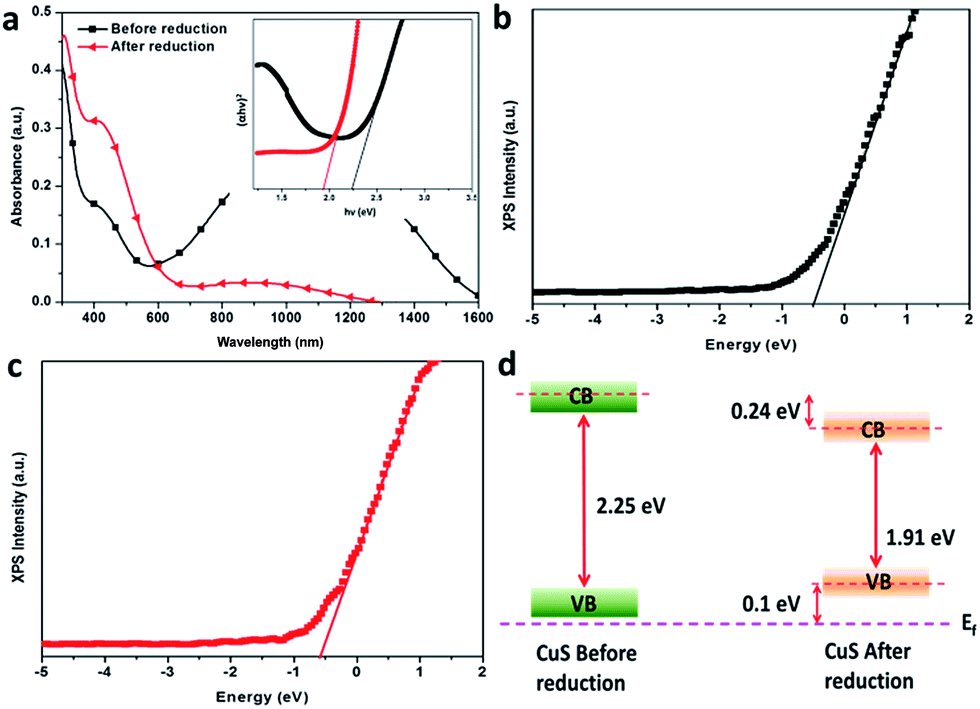 | ||
| Fig. 5 (a) UV-Vis spectra and corresponding Tauc analysis (inset) of CuS before (black line) and after (red line) reduction. XPS valence band edge spectra of (b) CuS before and (c) after electrochemical reduction. (d) Schematic band alignment position of CuS before and after electrochemical reduction constructed by optical and VB edge analysis. | ||
According to the literature, hydrogen strongly affects the electronic and structural properties of materials by binding to anions/cations (depending on type of semiconductors) or defects or other impurities.19 According to Van de Walle et al.,19 hydrogen exhibits qualitatively different behavior depending on the host semiconductor into which it is introduced. It can act either as a donor (H+) or an acceptor (H−) depending on the type of semiconductor. When hydrogen gas is introduced into semiconductors, hydrogen binds to the anionic species in p-type material, whereas it binds to the cationic species in n-type material.19 In the present case of CuS which is a p-type semiconductor, hence, it can be concluded that the hydrogen is assumed to bind to sulfide species instead of Cu. Since, the top of the valence band of CuS has a strong contribution from the sulfur p-orbitals and the bottom of the conduction band has contributions mainly from the Cu 4s and 4p orbitals and therefore, hydrogen binding to sulfide species mainly affects the valence band in the CuS system.20 This is in agreement with the absorbance and XPS data of sulfur.
Conclusions
In conclusion, pure covellite CuS thin films on ITO were prepared using a chemical bath deposition method. Our covellite CuS thin films exhibited a well-defined NIR absorption peak since the highest energy levels of valence band were populated with extra holes. The LSPR peak of CuS was tuned by reducing the hole concentration in the valence band. Hence, we systematically reduced the number of free holes in the valence band by means of electrochemical reduction. The green color of the CuS thin films was changed to brown after performing electrochemical reduction, and a periodic decrease in the NIR LSPR peak was observed. SEM and TEM analyses indicated that no changes were observed in the morphology and crystal structure of the covellite CuS thin films after valence band filling. XPS results concluded that the electrochemical reduction process changed the average sulfur valence from −1 to −2. This new strategy is simple and effective in tuning the LSPR property of CuS thin films.Acknowledgements
This research was supported by Nano Material Technology Development Program through the National Research Foundation of Korea (NRF) funded by the Ministry of Science, ICT and Future Planning (2009-0082580). This research is also supported by the Basic Science Program (2015R1A2A2A01003790) through NRF funded by MEST and ICT, Republic of Korea respectively. The fellowship awarded to S. K. was funded by the BK-plus program.Notes and references
- A. L. Routzahn, S. L. White, L. K. Fong and P. K. Jain, Isr. J. Chem., 2012, 52, 983–991 CrossRef CAS.
- S. Francesco, D. V. Giuseppe, R. S. K. Ajay, Z. Margherita, C. Alberto, L. Stefano, M. Liberato, L. Guglielmo and T. Francesco, Eur. Phys. J. B, 2013, 86, 154–174 CrossRef.
- Y. Xie, L. Carbone, C. Nobile, V. Grillo, S. D'Agostino, F. D. Sala, C. Giannini, D. Altamura, C. Oelsner, C. Kryschi and P. D. Cozzoli, ACS Nano, 2013, 7, 7352–7369 CrossRef CAS PubMed.
- M. Zhou, J. J. Li, S. Liang, A. K. Sood, D. Liang and C. Li, ACS Nano, 2015, 9, 7085–7096 CrossRef CAS PubMed.
- C. M. Hessel, V. P. Pattani, M. Rasch, M. G. Panthani, B. Koo, J. W. Tunnell and B. A. Korgel, Nano Lett., 2011, 11, 2560–2566 CrossRef CAS PubMed.
- W. H. Li, R. Zamani, P. R. Gil, B. Pelaz, M. Ibanez, D. Cadavid, A. Shavel, R. A. Alvarez-Puebla, W. J. Parak, J. Arbiol and A. Cabot, J. Am. Chem. Soc., 2013, 135, 7098–7101 CrossRef CAS PubMed.
- S. H. Wang, A. Riedinger, H. B. Li, C. H. Fu, H. Y. Liu, L. L. Li, T. L. Liu, L. F. Tan, M. J. Barthel, G. Pugliese, F. De Donato, M. S. D'Abbusco, X. W. Meng, L. Manna, H. Meng and T. Pellegrino, ACS Nano, 2015, 9, 1788–1800 CrossRef CAS PubMed.
- M. C. Brelle, C. L. Torres-Martinez, J. C. McNulty, R. K. Mehra and J. Z. Zhang, Pure Appl. Chem., 2000, 72, 101–117 CrossRef CAS.
- A. Comin and L. Manna, Chem. Soc. Rev., 2014, 43, 3957–3975 RSC.
- I. Kriegel, C. Jiang, J. Rodríguez-Fernández, R. D. Schaller, D. V. Talapin, E. Da Como and J. Feldmann, J. Am. Chem. Soc., 2012, 134, 1583–1590 CrossRef CAS PubMed.
- Y. Xie, A. Riedinger, M. Prato, A. Casu, A. Genovese, P. Guardia, S. Sottini, C. Sangregorio, K. Miszta, S. Ghosh, T. Pellegrino and L. Manna, J. Am. Chem. Soc., 2013, 135, 17630–17637 CrossRef CAS PubMed.
- W. Han, L. Yi, N. Zhao, A. Tang, M. Gao and Z. Tang, J. Am. Chem. Soc., 2008, 130, 13152–13161 CrossRef CAS PubMed.
- B. Sadtler, D. O. Demchenko, H. Zheng, S. M. Hughes, M. G. Merkle, U. Dahmen, L. W. Wang and A. P. Alivisatos, J. Am. Chem. Soc., 2009, 131, 5285–5293 CrossRef CAS PubMed.
- M. Kruszynska, H. Borchert, A. Bachmatiuk, M. H. Rummeli, B. Buchner, J. Parisi and J. Kolny-Olesiak, ACS Nano, 2012, 6, 5889–5896 CrossRef CAS PubMed.
- E. J. D. Garba and R. L. Jacobs, Physica B+C, 1986, 138, 253–260 CrossRef CAS.
- K. Laajalehto, I. Kartio, T. Kaurila, T. Laiho and E. Suoninen, Proc. 6th Eur. Conf. Appl. Surf. Interface Anal. ECASIA '95, ed. B. Reihl and D. Briggs, Wiley, New York, 1996 Search PubMed.
- S. S. Kalanur, Y. Lee and H. Seo, RSC Adv., 2015, 5, 9028–9034 RSC.
- P. Kumar, R. Nagarajan and R. Sarangi, J. Mater. Chem. C, 2013, 1, 2448–2454 RSC.
- C. G. Van de Walle and J. Neugebauer, Nature, 2003, 423, 626–628 CrossRef CAS PubMed.
- E. J. D. Garba and R. L. Jacobs, Physica B+C, 1986, 138, 253–260 CrossRef CAS.
| This journal is © The Royal Society of Chemistry 2017 |