
Synthesis of nanocrystalline Cu deficient CuCrO2 – a high figure of merit p-type transparent semiconductor
Leo
Farrell
*,
Emma
Norton
,
Christopher M.
Smith
,
David
Caffrey
,
Igor V.
Shvets
and
Karsten
Fleischer

School of Physics and Centre for Research on Adaptive Nanostructures and Nanodevices (CRANN), Trinity College, University of Dublin, Dublin 2, Ireland. E-mail: lefarrel@tcd.ie; Tel: +353 896 3808
First published on 24th November 2015
Abstract
The delafossite structured CuCrO2 system is well known as one of the best performing p-type transparent conducting oxides. In this paper the details of a low temperature facile growth method for CuCrO2 is described. The dependence of the growth on the precursors, the temperature and oxygen partial pressure are examined. The decomposition routes are critical to obtain the best performing films. The thermopower and electrical measurements indicate p-type films with conductivity ranging from 1–12 S cm−1 depending on the growth conditions. This p-type conductivity is retained despite the nanocrystallinity of the films. The figure of merit of these films can be as high as 350 μS, which is the best performing p-type TCO by solution methods to date. The optical properties are also investigated using ellipsometry and UV-Vis spectroscopy.
1 Introduction
Transparent conducting oxides (TCOs) are a material class used in flat screen displays, touch screens, organic light emitting diodes, and thin film solar cells as electrical contacts that are transparent to visible light. In terms of materials for such electronics, the oxides have become leading candidates as they show high transparency, high conductivity and their mobilities have surpassed amorphous and low temperature poly-crystalline silicon for display devices.1 The industry standard material is indium tin oxide (ITO) due to its high conductivity (≈1000 S cm−1) and transparency (>80%).2 The development of indium gallium zinc oxide (IGZO), a ternary oxide retaining mobility in its amorphous state, has allowed for commercial products utilizing IGZO as a transparent thin film transistor (TTFT) in the backplane of flat panel displays.3 IGZO has been essential for high dpi, low power, and 4 K high resolution displays.In contrast to the success of n-type oxides there is a limited number of high mobility p-type TCOs.4 To obtain the full functionality of oxide electronics technically feasible p-type TCOs are required. This lack of clear candidates for p-type transparent semiconductors demands further research. Without suitable n and p-type dopable materials active bi-polar devices using complementary metal oxide semiconductor (CMOS) technology for transparent electronics are not feasible. The noise immunity, low static power consumption and high density of logic functions arising from CMOS technology is therefore lost. Other uses of p-type TCOs include efficient charge injection layers for organic light emitting devices and solar cells with better band matching.5 The development of such a material is not a trivial task as the very nature of band structures limit the potential of most common oxides. n-type TCOs have rather high mobility typically related to the dispersion of the s orbitals that form their conduction bands. Doping can actually improve the transparency of the material close to the band edge, where the bottom of the conduction band is occupied and optical transitions require higher energies, an effect termed the Burstein–Moss shift, seen in degenerately doped TCOs. The curvature of the conduction band is close to parabolic and relatively low effective electron masses are obtained. By comparison most p-type TCOs have relatively flat valence bands with high hole effective masses. The discovery of a high mobility p-type TCO will allow for the design of new devices. Thus research into viable p-type TCOs is merited.
Cr-related oxides such as LaCrO3:Sr, CuCrO2, MnCr2O4:Li, and Cr2O3:Mg are an emerging class of p-type TCOs.6–8 It seems that the Cr 3d3 electron configuration is responsible for the p-type conductivity. Oxides with filled 3d10 orbitals such as the Cu delafossites have already been widely investigated. However, the forbidden d–d* transitions in non-filled 3d orbitals do not significantly limit the transmission in thin film form, opening up a range of candidate materials. CuCrO2 has been studied extensively as a p-type TCO. Crystalline CuCrO2 is a triangular lattice antiferromagnet, exhibiting the magnetoelectric effect.9,10 The material has also been investigated for its photocatalytic properties.11,12 p-type conductive films are obtained through intentional doping of the trivalent metal site (Ca, Mg, Ni),13–15 as crystalline stoichiometric CuCrO2 is typically highly resistive.13,16 High conductivity can be achieved with one claim of 220 S cm−1,14 although this has been difficult to reproduce with other growth methods. The highest conductivities after this value are for Mg doped samples on sapphire substrates synthesized by pulsed laser deposition (PLD) with conductivities in the 30–70 S cm−1 range.16–18 In contrast (excluding the report by Nagarajan et al.) most papers using amorphous substrates report conductivities in the 1–10 S cm−1 range.19,20 The transparency of these films is degraded by the doping; reduced to 40% for a 250 nm thick film. CuCrO2 has also been grown by other methods such as chemical vapor deposition (CVD), spray pyrolysis (SP), and sol–gel synthesis, although the performance of these films is significantly reduced in comparison to physical vapor deposition (PVD) methods.2,21–23
Recently our group has reported on the low temperature synthesis of Cu deficient CuCrO2 (CuxCrOy with x ≈ 0.5, y ≈ 2), schematically illustrated in Fig. 1.24 This was a single step method without the need for post-annealing or extrinsic doping, unlike previous reports. Due to the relatively low temperatures (≈345 °C) the Cu deficient material is compatible with flexible substrates (typically <400 °C process temperatures25). Additionally this is a cost effective method as the growth is performed by spray pyrolysis, an inexpensive technique that can achieve large area deposition, and uses the relatively abundant elements Cr and Cu. The films exhibit conductivities in the 1–12 S cm−1 range depending on the growth conditions, with optical transparencies of 55%.
 | ||
| Fig. 1 CuCrO2 lattice structure showing (a) the stoichiometric unit cell with the A and B layers highlighted. (b) Is a schematic CuxCrOy structure with a 1/3 Cu deficiency (Cu0.6CrO2). | ||
This Cu deficient CuCrO2 material is the best performing p-type TCO grown by solution methods to date. The material is therefore promising due to its straightforward fabrication that does not require crystal substrates, which is typical for high-performing p-type TCOs.26,27 This report is a detailed discussion of the chemical synthesis of these CuxCrOy films, the screening of the growth parameters to obtain the best-performing material, and finally a discussion on the retention of the p-type conductivity despite the nanocrystallinity of the films (which is in contrast to previous work28).
2 Experimental
Due to their stability in air and their relatively low toxicity the acetylacetonates (acac) are suitable precursors for SP.21 They are somewhat soluble in alcohol solvents such as methanol. Alcohol solvents are advantageous in SP if low cost air blast nozzles are employed, as they create droplets of smaller size than water-based solvents due to their lower density and surface tension. They also have lower boiling points which means they vaporize easily resulting in better pyrolytic decomposition.29 Cu(acac)2 and Cr(acac)3 precursors were dissolved in 100 ml of methanol solvent and sprayed with an air blast nozzle (PNR, model 0331) at a rate of 1.7 ml min−1 using a mixture of compressed air and nitrogen with an air pressure of 17 l min−1 onto heated glass microscope slides. Further details of the growth system are given elsewhere.24 The Cr(acac)3 concentration was typically kept constant at 0.025 M while the Cu(acac)2 concentration was varied up to 0.01 M. Heater surface temperature readings during spraying were taken using a type K thermocouple (chromel vs. alumel) welded to the top of the hot plate. The temperature was PID controlled during spray conditions within ±10 °C.The thickness of the films was determined from X-ray reflectivity (XRR) measurements. However for films >90 nm the films are too rough (>6 nm) to display X-ray interference fringes. In this case the thickness is determined from modeling UV-VIS reflectance measurements. The total UV-VIS transmittance and reflectance of the films were measured with a Perkin Elmer 650S spectrophotometer equipped with an integrating sphere. To determine the optical constants of the Cu deficient CuCrO2 material, a separate film has been grown on a silicon substrate to minimize the inter-facial roughness of the substrate. The thickness and roughness of the film was measured by XRR prior the optical analysis. Ellipsometric measurements were taken on a Sopra GESP5 at three angles close to the samples pseudo Brewster angle (66, 69, 72°). The measured tan![[thin space (1/6-em)]](https://www.rsc.org/images/entities/char_2009.gif) Ψ and cosΔ data have been modeled using the sample geometry as determined by XRR as an input parameter. The dielectric function was described by one 1D bulk critical point and two harmonic oscillators. The X-ray diffraction (XRD) pattern of the films was performed by a Bruker D8 Advance diffractometer using a Cu Kα source with a double bounce Ge monochromator. The glass background was subtracted from the data. The vibrational modes were measured by Micro-Raman spectroscopy in a Renishaw inVia system using a 532 nm solid state laser in backscattering geometry, which gives more information about the local bonding order. X-ray photoemission spectroscopy (XPS) measurements were performed on an Omicron Multiprobe XPS system using Al Kα X-rays (hν = 1486.7 eV) with an EA125 U5 analyzer. All samples were chemically cleaned in acetone and isopropanol with an ultrasonic bath and sputter-cleaned using an Ar ion gun operated at 500 V for 10 minutes with a sputter current of 2–3 μA (at low voltage to prevent oxygen sputtering) to remove traces of unreacted precursors precipitating after growth during sample cool down. Electrical conductivity measurements were performed using a linear four point probe geometry with gold coated tips. Seebeck measurements, performed as previously described,8 confirmed the p-type nature of the films.
Ψ and cosΔ data have been modeled using the sample geometry as determined by XRR as an input parameter. The dielectric function was described by one 1D bulk critical point and two harmonic oscillators. The X-ray diffraction (XRD) pattern of the films was performed by a Bruker D8 Advance diffractometer using a Cu Kα source with a double bounce Ge monochromator. The glass background was subtracted from the data. The vibrational modes were measured by Micro-Raman spectroscopy in a Renishaw inVia system using a 532 nm solid state laser in backscattering geometry, which gives more information about the local bonding order. X-ray photoemission spectroscopy (XPS) measurements were performed on an Omicron Multiprobe XPS system using Al Kα X-rays (hν = 1486.7 eV) with an EA125 U5 analyzer. All samples were chemically cleaned in acetone and isopropanol with an ultrasonic bath and sputter-cleaned using an Ar ion gun operated at 500 V for 10 minutes with a sputter current of 2–3 μA (at low voltage to prevent oxygen sputtering) to remove traces of unreacted precursors precipitating after growth during sample cool down. Electrical conductivity measurements were performed using a linear four point probe geometry with gold coated tips. Seebeck measurements, performed as previously described,8 confirmed the p-type nature of the films.
3 Results and discussion
The properties of the hitherto best performing nanocrystalline Cu deficient CuCrO2 films have been reported before by our group.24 The growth parameters to obtain these films and the chemistry involved are discussed here. To achieve good films a screening of the Cu precursor concentration, temperature, and oxygen partial pressure was performed. A Cu deficient CuCrO2 phase is obtained with a conductivity in the 1–5 S cm−1 for a Cu/(Cu + Cr) precursor ratio of ≈30% at 345 °C. This can be further improved by reducing the oxygen partial pressure during growth to 12 S cm−1. This screening of the growth conditions is discussed below.3.1 Growth of Cu deficient CuCrO2
During SP there are a number of processes occurring during film formation such as precursor solution atomization, solvent evaporation, drying and decomposition of the precursor salt, making it a complex system to model. Each precursor was initially tested separately to understand better the chemistry involved. Films grown with only the Cu precursor (0.01 M) result in predominately Cu2O films. XRD diffraction spectra of the Cu2O films show the expected reflexes for cuprous oxide, although it is difficult to discern the (200) peak from the background noise (see Fig. 2(a)). The coherent domain sizes evaluated by the Scherrer formula for these Cu2O layers was found to be 15 nm. The XRD pattern confirms that the films do not show the reflexes for CuO (35.5° and 39°). As the Cu2O phase is formed in these conditions it is likely that the formation of the delafossite structure, which needs Cu in its +1 oxidation state, is more probable. If the growth temperature was higher, CuO is more likely to form30 and therefore result in the unwanted CuCr2O4 spinel phase (Cu in +2 oxidation state) once the Cr precursor is added to the solution. Typically this phase needs to be dissolved by post-annealing at higher temperatures.22 However that can be directly avoided by inhibiting the formation of CuO and CuCr2O4 parasitic phases by using lower growth temperatures as demonstrated in this report. | ||
| Fig. 2 (a) XRD pattern of a film grown with Cu(acac)2 only, showing the expected reflexes for Cu2O. The pattern of a CuxCrOy film is shown in comparison. (b) Raman signal of Cr2O3 films grown by SP and by molecular beam epitaxy (MBE) compared to a CuxCrOy film grown at significantly lower temperatures. The strong A1g Cr2O3 vibrational mode is shown at 550 cm−1 with the dashed line. Dotted lines indicate the expected additional modes for CuCrO2. | ||
Films grown using just the Cr precursor (0.025 M) result in smooth insulating amorphous Cr2O3. However, significantly higher temperatures (>450 °C) are required to grow these Cr2O3 films. The heat stability of Cr(acac)3 is known to be greater than Cu(acac)2 and this may explain the higher temperatures required.31 These films show no XRD reflexes but the Cr2O3 vibrational modes were confirmed by Raman spectroscopy, see Fig. 2(b). For comparison epitaxial films of Cr2O3 grown by molecular beam epitaxy (MBE) on sapphire is shown. The strong A1g vibrational mode of Cr2O3 at ≈550 cm−1 is weaker in the SP films as expected as there is no observable crystallinity in the XRD spectra. The broad mode at 710 cm−1 is also related to the amorphous nature of the films and is caused by an increase in edge-sharing CrO6 octahedra, also observed in other amorphous materials and CuCrO2.32
When the two precursors are mixed the resulting films are a conductive mixed CuxCrOy phase, even at the low temperature conditions. There is a dependency of the growth rate on the Cu content in the films, illustration that the film formation is limited by the presence of the Cu precursor. This is shown in Fig. 3, where the growth rate is plotted as a function of the nominal Cu content. The growth rate is calculated by measuring the thickness ex situ using XRR and recording the growth time. The nominal Cu content refers to the precursor ratio in the solution prior to deposition while the actual atomic Cu/(Cu + Cr) ratio was determined by using XPS. Without the presence of Cu no film growth is observed for the Cr precursor up to temperatures of 450 °C. However once a small amount of Cu is included the growth rate increases and films best described as highly defective, nanocrystalline delafossite CuCrO2 are formed. The incorporated Cu content is significantly higher and quickly saturates around 30% corresponding to a Cu0.43CrO2 stoichiometry. See Fig. 4 for the development of the CuCrO2 XRD reflexes. Above 22% of nominal Cu content, both XRD peaks at 36.3° and 62.2° are consistent with the (012) and (110) XRD diffraction peaks of delafossite CuCrO2, which is a rhombohedral crystal cell with space group R![[3 with combining macron]](https://www.rsc.org/images/entities/char_0033_0304.gif) m. Using the MAUD software package and the CuCrO2 cif file (PDF number 01-089-6744), the a and c lattice parameters were calculated to be 2.98 ± 0.05 Å and 17.16 ± 0.05 Å respectively, with an average coherent domain size of 7 ± 3 nm, suggesting nano-crystallinity. The delafossite structure consists of edge-sharing octahedral layers (CrO6 – A layer), stacked between linearly coordinated Cu atoms in an O–Cu–O dumbbell shape (B layer). This stacking is along the c-axis of the crystal lattice as shown in Fig. 1.33 However as the thickness is limited by the Cu content the AB stacking only occurs when there is enough Cu being decomposed to fill the lattice structure. The growth rate is also influenced by the molarity of the solution as shown in Fig. 3(b). For an increased chromium concentration and a fixed nominal Cu/(Cu + Cr) ratio the growth rate also increases as there is a greater number of Cu atoms present in the solution. The chromium concentration was typically kept at 0.025 M.
m. Using the MAUD software package and the CuCrO2 cif file (PDF number 01-089-6744), the a and c lattice parameters were calculated to be 2.98 ± 0.05 Å and 17.16 ± 0.05 Å respectively, with an average coherent domain size of 7 ± 3 nm, suggesting nano-crystallinity. The delafossite structure consists of edge-sharing octahedral layers (CrO6 – A layer), stacked between linearly coordinated Cu atoms in an O–Cu–O dumbbell shape (B layer). This stacking is along the c-axis of the crystal lattice as shown in Fig. 1.33 However as the thickness is limited by the Cu content the AB stacking only occurs when there is enough Cu being decomposed to fill the lattice structure. The growth rate is also influenced by the molarity of the solution as shown in Fig. 3(b). For an increased chromium concentration and a fixed nominal Cu/(Cu + Cr) ratio the growth rate also increases as there is a greater number of Cu atoms present in the solution. The chromium concentration was typically kept at 0.025 M.
 | ||
| Fig. 3 (a) The dependence of the growth rate on the nominal Cu content in the initial solution. The growth is limited by the presence of the Cu precursor. (b) Once a minimum Cu/Cr ratio is present, the growth rate increases for an increased total molarity of solution. | ||
 | ||
| Fig. 4 XRD pattern of films for different nominal Cu content. XRD reflexes are indexed for CuCrO2 (PDF-00-039-0247). | ||
Fig. 5(e) shows the XPS spectra of the Cu-precursor (Cu(acac)2) itself, which matches previously published data on Cu(acac)2.34 The copper region of the CuxCrOy films shows Cu in a +1 oxidation state with a mixture of the unreacted Cu precursor present (Fig. 5(a)). The unreacted precursor is likely to be deposited at the surface after the growth during sample cool-down from residual vapors in the chamber. After the initial cleaning step the precursor traces are removed, while the Cu+1 signature of the oxide material remains unchanged (Fig. 5(c)). The disappearance of the unreacted precursor after short Ar sputtering confirms that it is not incorporated in the film in the unreacted form. The XPS Cu content shows that the films typically are Cu deficient with a Cu/(Cu + Cr) ratio of ≈33%, even if the nominal Cu content is lower. Therefore the Cu deficient phase forms and further growth is limited by the lack of Cu. The growth most likely proceeds by a stacking of the A (CrO6) and B (O–Cu–O) layers as show in Fig. 6.
 | ||
| Fig. 5 (a and b) Shows the XPS spectra of both the Cu and Cr regions of the as received CuxCrOy sample. (c and d) Is after typical cleaning conditions cleaned using an Ar ion gun operated at 500 V for 10 minutes with a sputter current of 2–3 μA. (e) Is the XPS spectra of the unreacted Cu(acac)2 precursor. There is no evidence of the shake-up satellite peaks expected between 940–945 eV for Cu in its +2 oxidation state after the unreacted precursor is removed. | ||
 | ||
| Fig. 6 Growth diagram showing the spray configuration and a schematic of the atomic growth process. | ||
Insufficient Cu would prevent the formation of the dumbbell linkages in the B layer. Growth occurs even when the direct line of sight of the nozzle to the substrate is blocked, which suggest that the growth proceeds by a chemical vapor deposition (CVD)-like process. Our growth model is supported by recent studies on ALD growth of CuCrO2.35 The adsorption and reaction of the Cr(acac)3 is self limited, at the low temperatures used here and in ALD. This explains the low growth rates of Cr2O3 in the absence of the Cu precursor. Once a Cr terminated surface is completed further Cr adsorption is inhibited. The Cu precursor does readily react with the Cr terminated surface and once the surface is sufficiently Cu terminated so does the Cr precursor. Hence the natural A–B layered stacking is continuously maintained. This growth mode also explains the significant difference in actual film composition and nominal Cu/Cr ratio as the growth is always limited by the need to achieve a high Cu coverage prior Cr adsorption.
The films have low roughness and are homogeneous, as expected for a CVD-like growth. In this case the solvent evaporates, followed by the vaporization of the precursors (the acac precursors are reasonably volatile21) and the diffusion of the vapor to the substrate where an oxide is formed, see Fig. 6. Previous studies have discussed the SP growth in terms of decomposition of the precursors followed by a chemical reaction between the Cu and Cr oxides on the surface of the substrate.22,23 As this was at the higher temperature of 550 °C the growth processes discussed here are likely to be different.
Interestingly the films do not tend towards a Cu/(Cu + Cr) ratio of 50% as would be expected for a stoichiometric CuCrO2 phase. Fig. 1(b) shows the possible lattice structure for 1/3 Cu deficiency (Cu/(Cu + Cr) ratio of 33%). The image is only illustrative and does not account for a possible relaxation of the atomic lattice positions. The Cr:Cu:O ratio from XPS is approximately 1:2:4 which would indicate that the atomic ratio is close to the spinel phase of copper chromite (CuCr2O4). However as shown in Fig. 5 the expected shake-up satellite peaks between 940–945 eV for the Cu+2 oxidation state is absent, which is the oxidation state of Cu in the spinel phase. The XPS shows that Cu related peak present is at a binding energy of 932.4 eV as expected for the Cu+1 oxidation state. Similarly the binding energy of the Cr 2p3/2 is 576.6 eV, indicating a +3 oxidation state, which is consistent with previous reports for CuCrO2.36,37
The combined analysis in terms of charge states for Cu and Cr, the XRD and Raman analysis and the quantitative analysis of the Cu/Cr ratio throughout the films leads to our assessment that the films are homogeneous and closely related to the delafossite structure. The copper deficiency can either be explained by a certain amount of Cu vacancies, or additional Cr within the B-layers in combination with oxygen interstitials. The high number of defects and the consequently poor crystallinity of the films makes a quantitative analysis difficult. Qualitative comparison with CuCrO2 crystalline nanoparticles highlights this as the measured Raman modes in the CuxCrOy films are substantially broader than even in 10 nm small crystalline nanoparticles38 (see Fig. 2). The presence of defined XRD reflexes combined with the absence of sharp Raman modes suggest a certain long range order of crystallographic planes with a high local disorder in the atomic bonds.
3.2 Temperature dependence
The substrate temperature is a crucial parameter in SP as it contributes to aerosol generation, solvent evaporation and precursor decomposition.39 There is a particular optimum temperature range for a given Cu/(Cu + Cr) precursor ratio which is related to the vaporization of the precursors followed by oxide formation on the substrate induced by the temperature of the heater. Fig. 7 shows the dependence of the figure of merit (FOM) for a fixed nominal Cu content of 30%. The FOM used is defined as: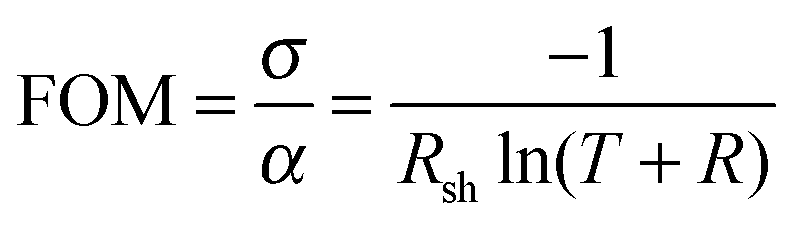 | (1) |
 | ||
| Fig. 7 (a) Shows the dependence of the FOM on the growth temperature for a fixed nominal Cu content of 30%. (b) The dependence of the conductivity on the oxygen partial pressure. A reduced oxygen partial pressure results in higher conductivity samples. (c) Shows the sum of the total transmittance and total reflectance is plotted as a function of energy. A photograph of a representative sample (90 nm) is shown in the inset to demonstrate visual transparency. | ||
3.3 Oxygen partial pressure dependence
The conductivity of the films was influenced by the oxygen partial pressure in the chamber during growth. A low oxygen pressure environment is essential for the most conductive films. Pre-evacuation of the growth chamber is required to remove residual oxygen by purging with nitrogen gas. If there is an oxygen rich environment present during the start of the growth then the formation of Cr2O3 is favored, as it is the more thermodynamically stable phase.To understand better the phase purity of the material and the dependence on oxygen partial pressure, depth profiling was performed. This was done using an Ar+1 ion gun operated at a higher voltage of 750 V with a sputter current of 8.5 μA. The atomic ratio was taken at each interval. After sputtering for 10, 33 and 60 minutes the Cu+1 and Cr+3 line-shapes do not change significantly. With XRR thickness measurements before and after sputtering the effective sputter rate was estimated to be 0.35 nm min−1, while the initial cleaning step at lower voltage does not lead to a significant oxide removal. Fig. 8 shows the oxygen partial pressure in the chamber with no pre-evacuation (a) and after evacuation (b). The corresponding XPS determined ratios as a function of etch time are shown in Fig. 8(c) and (d) corresponding to (a) and (b) respectively. The ratios indicate that in the low oxygen environment Cu deficient CuCrO2 (≈33% Cu/(Cu + Cr) ratio) is formed, while in the oxygen rich condition a predominately Cr2O3 rich phase is present.
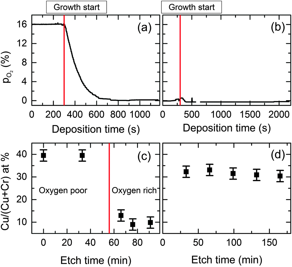 | ||
| Fig. 8 (a) The oxygen partial pressure during growth for a non-evacuated chamber. (b) The oxygen partial pressure during growth for an evacuated chamber. (c) The corresponding XPS determined Cu/(Cu + Cr) atomic ratio for (a) showing the lower Cu content in the oxygen rich conditions as a function of etch time. The oxygen rich area is at the bottom of the film and is revealed after longer etch time. (d) The XPS ratio showing a consistent Cu content throughout the film. | ||
A low oxygen content in the carrier gas also leads to higher conductivities as demonstrated in Fig. 7. Previously compressed air was used during growth, but reducing the oxygen content by introducing a mix of nitrogen in the carrier gas leads to more conductive CuxCrOy. The optimum nominal oxygen partial pressure in the carrier gas is around 5% before the conductivity drops again. In very low oxygen partial pressure the films do not have enough oxygen to form oxides and the precursors are left on the surface of the substrate.
In summary, growth conditions for the CuxCrOy phase have to be optimised to avoid the formation of potential parasitic, non conducting phases in particular the CuCr2O4 spinel phase. In low oxygen conditions the decomposition and surface adsorption of the Cr(acac)3 precursor is sufficiently inhibited and the growth is limited by the prerequisite of the Cu(acac2) adsorption. This mechanism leads to a significantly higher Cu content in the grown films than nominally present in the solution, saturating at a optimum stoichiometry of Cu0.4CrO2.5. The optimum nominal Cu/Cr ratio in the solution is a function of temperature and oxygen partial pressure. At higher temperature, or if more oxygen is present the film composition is closer to the nominal Cu/Cr ratio suggesting the formation of a material closer related to amorphous Cr2O3:Cu. At higher temperatures the crystallinity improves to be on par with previously spray pyrolysis synthesised Cr2O3:Mg, however the conductivity of such films are 2–3 orders of magnitude lower than for the CuxCrOy phase grown at lower temperatures.
3.4 Optical properties
The sum of the total transmittance and total reflectance is plotted as a function of energy for 80 nm film in Fig. 7. The reflectivity of the films is high, with the reflectance as large as 25%. The reflectance loss can be mitigated by an anti-reflective layer if the films were used in a stacked layer. The transparency is still relatively high, with around 55% for similar thicknesses. The high transparency of the material is another indication that the phase is not CuCr2O4 as the spinel phase has been found to be very absorbent, even in thin film form.40The highest FOM of these films is 350 μS surpassing the previous value of 151 μS.5 This FOM can favor high conductivity, low transparency films. However the Haacke's FOM(〈T〉10/Rsh) penalizes lower transparency material, and our films exhibit values of 1.5 × 10⁻⁷ comparable with the highest reported Haacke's FOM for a delafossite. As these films can be deposited at relatively low temperature and on amorphous substrates (which gives it further advantages in industrial process considerations), this material is competitive with the majority of available p-type TCOs.
Transmission and reflectance measurements can be quickly measured and are helpful to assess the figure of merit of TCOs in general. Great care however has to be taken in order to extract optical parameters of thin films out of such measurements. This is because transmission measurements are not sensitive to small changes in the refractive index and variations in film thickness, or to roughness and scattered losses in polycrystalline material. Incorrect referencing can also systematically skew results. Direct calculations of n and k are therefore error prone and lead to large variations in reported values of refractive index.41 To assess the optical constants of the Cu deficient CuCrO2 properly we deposited a similar film on crystalline silicon substrates to minimize interface roughness as well as on glass. The film thickness was determined independently by XRR. Ellipsometric measurements on these films were used to model the optical constants of the films, the derived optical constant were then used to model the normal incidence transmission and reflectance measurements on samples deposited on glass to assess the consistency of the results. Fig. 9 compares n and k of Cu0.4CrO2 with published data of crystalline Cr2O3 and CuCrO2.42,43 The reference data chosen were similarly measured by ellipsometry on smooth polycrystalline thin films allowing for a more systematic comparison. As seen by the increased k, the Cu deficient CuCrO2 is significantly more absorbing in the visible range than both crystalline materials, yet transparent enough for a high figure of merit. The onset of the fundamental absorption in CuCrO2 is lower than Cr2O3. In Mg doped crystalline CuCrO2 (where doping is required to improve the electrical performance) it is already known that the absorption is significantly higher. For samples of similar conductivity, the absorbance between 2–3 eV can be up to three times higher compared to low doped samples.44 This is in line with our k-values for Cu deficient CuCrO2. This indicates that the Mg-doping introduces deeper mid gap states as well as increased Urbach energies very similar to those introduced by intrinsic defects in our films. This not only explains the good electrical performance of our films but also indicates that defect complexes of Mg in conjunction with adjacent intrinsic defects are crucial to understand crystalline CuCrO2 itself.
 | ||
| Fig. 9 Comparison of the n and k for Cu deficient CuCrO2 with published data of crystalline Cr2O3 and CuCrO2 included.42,43 | ||
3.5 Electrical and thermoelectrical measurements
Hall effect measurements were performed on the films using a 12 T magnetic field and contacts in the Van der Pauw configuration. However it was not possible to extract a reliable Hall signal to obtain a mobility value. This would set an upper limit of ≈0.1 cm2 V−1 s−1 on the mobility. The Bosman and van Daal limit of 0.1 cm2 V−1 s−1 would suggest that the transport in these films is limited by small polaron hopping (SPH).45 The SPH model has already been applied to CuCrO2 as it is known as a polaronic material.46 In this scenario free electrons/holes tend to form polarons due to the high electron–phonon coupling. A polaron is the charge carrier, and its collective influence on the surrounding charge state, which moves sluggishly in comparison to the band conductor's free carrier picture. The SPH conductivity can be expressed as: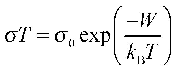 | (2) |
 | ||
| Fig. 10 (a) The small polaron conductivity dependence on temperature for samples with and without optimized oxygen partial pressure. The inset shows the VRH conductivity. The dashed line in both plots indicates 220 K is the approximate cross over in the conduction mechanism. (b) A Jonker's plot showing the decrease in the Seebeck coefficient with conductivity. Previous work is displayed in red.43 Electrical and thermoelectrical transport values for films grown at different oxygen partial pressures are given below. | ||
The Seebeck coefficient was measured for these films, ranging from 70–100 μV K−1. Undoped crystalline CuCrO2 is usually insulating, but these films can be quite conductive (up to 12 S cm−1). The Cu deficiency in the material can lead to acceptor like defects which could be responsible for the conductivity. Retention of the p-type conductivity despite the nanocrystallinity of the films is advantageous as it means that amorphous substrates can be used. The p-type conductivity is not lost as a result of using amorphous substrates contrary to previous reports.45 In fact the films behave similarly to Mg doping in crystalline films; the Seebeck coefficient is reduced for increasing conductivity. A Jonker plot is shown in Fig. 10(b) showing the dependence of the Seebeck coefficient on the conductivity. Data from previous work43 is plotted as well to show the similarity between Cu deficient films and previous work. Using the band conductor model for semiconductors the Seebeck coefficient can be related to the conductivity by:47
 | (3) |
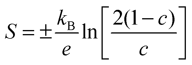
The Seebeck coefficient can be used to estimate the mobility of thin films within the SPH model.8,48 The Seebeck coefficient S is related to the is the fraction of occupied carrier sites c by:
 | (4) |
 | (5) |
However an alternate version of the formula, which factors in the degeneracy gives 0.03 cm2 V−1 s−1, an order of magnitude larger.43 It is likely that the mobility lies within the upper boundary set by the Hall mobility measurements and the lower boundary set by the SPH mobility model used here, 0.006–0.1 cm2 V−1 s−1. As discussed recently devices such as rectifiers, photodetectors and n-type junction field-effect transistors are not adversely affected by low p-type mobility.6
4 Conclusion
This Cu deficient CuCrO2 material is the best performing p-type TCM grown by solution methods to date (excluding reports on single-crystal substrates49). This is despite the relatively low processing temperatures and the solution based technique used. In this report the dependence of the electrical and optical properties on the Cu content, the temperature, and the oxygen partial pressure is examined. The growth of the CuxCrOy films and its close relation to the delafossite CuCrO2 phase is discussed, followed by characterization of the optical and electrical properties. The mobility of the holes is estimated from thermoelectrical measurements of the films. The presented spray pyrolysis synthesis using organic salts and solvents provides a facile method to obtain a high-performing p-type TCO, compatible with flexible substrates.Acknowledgements
Financial support by Science Foundation Ireland under grant No. 12/IA/1264 and grant No. 12/RC/2278 is gratefully acknowledged. This work was supported by the Higher Education Authority under the PRTLI scheme, cycle 5. Funding support from the Irish Research Council under grant no. GOI/PG/2013/445 is also acknowledged.References
- J. C. Park, H.-N. Lee and S. Im, ACS Appl. Mater. Interfaces, 2013, 5, 6990–6995 CAS.
- Z. Chen, W. Li, R. Li, Y. Zhang, G. Xu and H. Cheng, Langmuir, 2013, 29, 13836–13842 CrossRef CAS PubMed.
- T. Kamiya, K. Nomura and H. Hosono, Sci. Technol. Adv. Mater., 2010, 11, 044305 CrossRef.
- G. Hautier, A. Miglio, G. Ceder, G.-M. Rignanese and X. Gonze, Nat. Commun., 2013, 4, 2292 Search PubMed.
- M. Aksit, S. K. Kolli, I. M. Slauch and R. D. Robinson, Appl. Phys. Lett., 2014, 104, 161901 CrossRef.
- K. H. L. Zhang, Y. Du, A. Papadogianni, O. Bierwagen, S. Sallis, L. F. J. Piper, M. E. Bowden, V. Shutthanandan, P. V. Sushko and S. A. Chambers, Adv. Mater., 2015, 27, 5191–5195 CrossRef CAS PubMed.
- A. R. Nagaraja, K. H. Stone, M. F. Toney, H. W. Peng, S. Lany and T. O. Mason, Chem. Mater., 2014, 26, 4598–4604 CrossRef CAS.
- L. Farrell, K. Fleischer, D. Caffrey, D. Mullarkey, E. Norton and I. V. Shvets, Phys. Rev. B: Condens. Matter Mater. Phys., 2015, 91, 125202 CrossRef.
- K. Kimura, H. Nakamura, S. Kimura, M. Hagiwara and T. Kimura, Phys. Rev. Lett., 2009, 103, 107201 CrossRef CAS PubMed.
- K. Kimura, H. Nakamura, K. Ohgushi and T. Kimura, Phys. Rev. B: Condens. Matter Mater. Phys., 2008, 78, 140401 CrossRef.
- W. Ketir, A. Bouguelia and M. Trari, J. Hazard. Mater., 2008, 158, 257–263 CrossRef CAS PubMed.
- S. Saadi, A. Bouguelia and M. Trari, Sol. Energy, 2006, 80, 272–280 CrossRef CAS.
- F. Benko and F. Koffyberg, Mater. Res. Bull., 1986, 21, 753–757 CrossRef CAS.
- R. Nagarajan, A. D. Draeseke, A. W. Sleight and J. Tate, J. Appl. Phys., 2001, 89, 8022–8025 CrossRef CAS.
- S. Y. Zheng, G. S. Jiang, J. R. Su and C. F. Zhu, Mater. Lett., 2006, 60, 3871–3873 CrossRef CAS.
- M. O'Sullivan, P. Stamenov, J. Alaria, M. Venkatesan and J. M. D. Coey, J. Phys.: Conf. Ser., 2010, 200, 052021 CrossRef.
- U. Sidik, H. Y. Lee and J.-Y. Lee, J. Nanosci. Nanotechnol., 2015, 15, 5163–5166 CrossRef CAS PubMed.
- D. Li, X. Fang, Z. Deng, W. Dong, R. Tao, S. Zhou, J. Wang, T. Wang, Y. Zhao and X. Zhu, J. Alloys Compd., 2009, 486, 462–467 CrossRef CAS.
- Q. Meng, S. Lu, S. Lu and Y. Xiang, J. Sol–Gel Sci. Technol., 2012, 63, 1–7 CrossRef CAS.
- R. Bywalez, S. Gotzendorfer and P. Lobmann, J. Mater. Chem., 2010, 20, 6562–6570 RSC.
- S. Mahapatra and S. A. Shivashankar, Chem. Vap. Deposition, 2003, 9, 238 CrossRef CAS.
- S. H. Lim, S. Desu and A. C. Rastogi, J. Phys. Chem. Solids, 2008, 69, 2047–2056 CrossRef CAS.
- A. C. Rastogi, S. H. Lim and S. B. Desu, J. Appl. Phys., 2008, 104, 023712 CrossRef.
- L. Farrell, E. Norton, B. J. O'Dowd, D. Caffrey, I. V. Shvets and K. Fleischer, Appl. Phys. Lett., 2015, 107, 031901 CrossRef.
- M.-G. Kim, M. G. Kanatzidis, A. Facchetti and T. J. Marks, Nat. Mater., 2011, 10, 382–388 CrossRef CAS PubMed.
- S. Wang, L. Sun, H. Zhang, D. Elhadj, J. Wang and G. Fu, Opt. Mater. Express, 2014, 4, 2209–2214 CrossRef.
- H. Hiramatsu, K. Ueda, H. Ohta, M. Hirano, M. Kikuchi, H. Yanagi, T. Kamiya and H. Hosono, Appl. Phys. Lett., 2007, 91, 012104 CrossRef.
- S. Narushima, H. Mizoguchi, K. Shimizu, K. Ueda, H. Ohta, M. Hirano, T. Kamiya and H. Hosono, Adv. Mater., 2003, 15, 1409–1413 CrossRef CAS.
- P. S. Patil, Mater. Chem. Phys., 1999, 59, 185–198 CrossRef CAS.
- L. D. L. S. Valladares, D. H. Salinas, A. B. Dominguez, D. A. Najarro, S. Khondaker, T. Mitrelias, C. Barnes, J. A. Aguiar and Y. Majima, Thin Solid Films, 2012, 520, 6368–6374 CrossRef CAS.
- J. V. Hoene, R. G. Charles and W. M. Hickam, J. Phys. Chem., 1958, 62, 1098–1101 CrossRef.
- H. C. Barshilia, N. Selvakumar, K. S. Rajam and A. Biswas, J. Appl. Phys., 2008, 103, 023507 CrossRef.
- C. T. Prewitt, R. D. Shannon and D. B. Rogers, Inorg. Chem., 1971, 10, 719 CrossRef.
- K. Okada, J. Kawai and A. Kotani, Phys. Rev. B: Condens. Matter Mater. Phys., 1993, 48, 10733–10738 CrossRef CAS.
- T. S. Tripathi, J.-P. Niemelä and M. Karppinen, J. Mater. Chem. C, 2015, 3, 8364–8371 RSC.
- M. C. Biesinger, L. Lau, A. R. Gerson and R. S. C. Smart, Appl. Surf. Sci., 2010, 257, 887 CrossRef CAS.
- H. Y. Chen and C. C. Yang, Surf. Coat. Technol., 2013, 231, 277–280 CrossRef CAS.
- T.-W. Chiu, B.-S. Yu, Y.-R. Wang, K.-T. Chen and Y.-T. Lin, J. Alloys Compd., 2011, 509, 2933–2935 CrossRef CAS.
- D. Perednis and L. Gauckler, J. Electroceram., 2005, 14, 103–111 CrossRef CAS.
- H. Sun, M. A. P. Yazdi, P. Briois, J.-F. Pierson, F. Sanchette and A. Billard, Vacuum, 2015, 114, 101–107 CrossRef CAS.
- D. Poelman and P. F. Smet, J. Phys. D: Appl. Phys., 2003, 36, 1850 CrossRef CAS.
- P. Hones, M. Diserens and F. Levy, Surf. Coat. Technol., 1999, 120–121, 277–283 CrossRef CAS.
- A. Barnabe, Y. Thimont, M. Lalanne, L. Presmanes and P. Tailhades, J. Mater. Chem. C, 2015, 3, 6012–6024 RSC.
- X. Li, M. Han, X. Zhang, C. Shan, Z. Hu, Z. Zhu and J. Chu, Phys. Rev. B: Condens. Matter Mater. Phys., 2014, 90, 035308 CrossRef.
- A. R. Nagaraja, N. H. Perry, T. O. Mason, Y. Tang, M. Grayson, T. R. Paudel, S. Lany and A. Zunger, J. Am. Ceram. Soc., 2012, 95, 269–274 CrossRef CAS.
- D. O. Scanlon and G. W. Watson, J. Mater. Chem., 2011, 21, 3655–3663 RSC.
- Q. Zhu, E. M. Hopper, B. J. Ingram and T. O. Mason, J. Am. Ceram. Soc., 2011, 94, 187–193 CrossRef CAS.
- N. Mansourian-Hadavi, S. Wansom, N. H. Perry, A. R. Nagaraja, T. O. Mason, L.-h. Ye and A. J. Freeman, Phys. Rev. B: Condens. Matter Mater. Phys., 2010, 81, 075112 CrossRef.
- R. Wei, X. Tang, L. Hu, Z. Hui, J. Yang, H. Luo, X. Luo, J. Dai, W. Song, Z. Yang, X. Zhu and Y. Sun, Chem. Commun., 2014, 50, 9697–9699 RSC.
| This journal is © The Royal Society of Chemistry 2016 |