
Effects of the radio-frequency sputtering power of an MgO tunneling barrier on the tunneling magneto-resistance ratio for Co2Fe6B2/MgO-based perpendicular-magnetic tunnel junctions†
Du-Yeong
Lee
a,
Hyung-Tak
Seo
b and
Jea-Gun
Park
*a
aDepartment of Electronics and Computer Engineering, MRAM Center, Hanyang University, Seoul, 133-791, Republic of Korea. E-mail: parkjgL@hanyang.ac.kr
bDepartment of Energy Systems Research & Materials Science and Engineering, Ajou University, Suwon 443-739, Republic of Korea. E-mail: hseo@ajou.ac.kr
First published on 23rd November 2015
Abstract
For Co2Fe6B2–MgO based p-MTJ spin valves with [Co/Pt]n–SyAF layers ex situ annealed at 350 °C and 30 kOe for 30 min, the tunneling magneto-resistance (TMR) ratio strongly depended on the radio-frequency (RF) sputtering power in a 0.65–1.15 nm thick MgO tunneling barrier, achieving a TMR ratio of 168% at 300 W. The TMR ratio rapidly and linearly increased with a decrease in the RF sputtering power between 300 and 500 W and then abruptly decreased at 250 W since the face-centered-cubic crystallinity of the tunneling barrier improved with a decrease in the RF sputtering power between 300 and 500 W and then abruptly degraded at 250 W. Optical properties measured by spectroscopic ellipsometry, such as the defect state density and energy band gap of a ∼1.0 nm thick tunneling barrier layer, indicate that the RF sputtering power needed to obtain a larger poly grain size for the barrier tends to enhance the barrier's face-centered-cubic crystallinity.
Introduction
With the aim of developing a terabit integrated nonvolatile memory cell, many researchers have intensively studied perpendicular spin-transfer torque magnetic random access memory (p-STT MRAM) cells because of their fast write time (∼10 ns), non-volatile memory operation, extremely low power consumption, and no scaling-down limit of less than 20 nm.1,2 A p-STT MRAM cell consists of a selective device (such as an n-MOSFET, p–n diode, p–n–p diode, or an ovonic threshold device) and a perpendicular magnetic tunnel junction (p-MTJ) spin valve. In particular, CFB (Co2Fe6B2 or Co4Fe4B2)/MgO based p-MTJ spin valves have been widely studied since they have demonstrated excellent device performance characteristics. These include a high tunneling magneto-resistance (TMR) ratio of ∼150%, a high thermal stability (Δ = E/kBT) of 74, and a low critical current density (JC0) of 13.4 MA cm−2 where E, kB, and T are respectively the energy barrier, the Boltzmann constant, and the temperature.1,3 Key issues for obtaining a higher TMR ratio in CFB/MgO-based p-MTJ spin-valves are (1) the interfacial-perpendicular magnetic anisotropy (i-PMA) between the free or pinned Co2Fe6B2 layer and the MgO tunneling barrier and (2) the tunneling barrier's face-centered-cubic (fcc) crystallinity.4–8 Note that the achievement degree of i-PMA characteristics is determined by the hybridization of Fe3d–O2p and Co3d–O2p at the Co2Fe6B2–MgO interface, which is directly affected by the interface body-centered-cubic (bcc) crystallinity of the free and pinned Co2Fe6B2 layer, the tunneling barrier fcc crystallinity, and the ex situ magnetic annealing temperature.9–12 In addition, since CFB/MgO-based p-MTJ spin valves should achieve an excellent device performance at the back-end-of-line temperature of ∼350 °C,13 the tunneling barrier crystallinity becomes more and more critical at a higher ex situ magnetic annealing temperature. Thus, in our study, in order to obtain the best crystallinity in an MgO tunneling barrier at an ex situ magnetic annealing temperature greater than 350 °C, we investigated how the radio-frequency (RF) sputtering power of a 0.65–1.15 nm thick MgO tunneling barrier affects the TMR ratio and the resistance-area (RA) product for p-MTJ spin valves by using a current-in-plane tunneling (CIPT) technique,14 and how it affects the tunneling barrier crystallinity by using cross-sectional transmission electron microscopy (x-TEM). In addition, we observed the dependency of the static magnetization behavior of p-MTJ spin valves on the tunneling barrier RF power. Finally, we correlated the crystallinity of the MgO tunneling barrier of ∼1.0 nm via x-TEM images with optical properties via high resolution spectroscopic ellipsometry (SE)15,16 to understand how the RF power affects the crystallinity of the MgO tunneling barrier.Experimental
We prepared Co2Fe6B2–MgO-based p-MTJ spin valves with [Co/Pt]n–SyAF layers by using a 12 inch-wafer multi-chamber cluster magnetron sputtering system with 5 inch-diameter targets under a high vacuum of less than 1 × 10⁻⁸. Specifically, the valves were fabricated on 12 inch wafers with a vertical W/TiN bottom electrode/Ta buffer layer/b.c.c seed layer (2.0 nm)/Co2Fe6B2 (1.05 nm) free layer/MgO (tMgO = 0.6–1.15 nm structure under an RF power of 250, 300, 350, 400, 450, and 500 W) tunneling barrier/Fe (0.4 nm)/Co2Fe6B2 (1.0 nm) pinned layer/b.c.c capping layer (0.6 nm)/Co/Pt buffer layer/([Co/Pt]5/Co) lower SyAF layer/Ru spacer layer/(Co/Pt/[Co/Pt]6) upper SyAF layer/Ta/Ru top electrode. The DC power of Co2Fe6B2, Ta, b.c.c metal, Co, and Pt were 250, 300, 150, 300, and 100 W, respectively. The b.c.c seed and capping layer have a lattice constant of 3.16 Å.3 In addition, a 0.4 nm thick Fe layer was inserted between the MgO tunneling barrier and the Co2Fe6B2 pinned layer to obtain a higher TMR ratio.27 In particular, we performed twice in situ annealing at 400 °C for 30 min after MgO tunnel barrier and b.c.c capping layer sputtering to obtain a higher TMR ratio of the p-MTJ spin-valve via enhancing the i-PMA characteristics at both the free and pinned Co2Fe2B6 layers, see the ESI† S1. Finally, after Ru electrode sputtering, we performed ex situ annealing at 350 °C for 30 min under vacuum below 10−6 Torr and a perpendicular magnetic field of 30 kOe, as shown in Fig. 1(a). We used the CIPT technique to estimate the TMR ratio and RA for all 12 inch wafers fabricated with Co2Fe6B2–MgO based p-MTJ spin valves with [Co/Pt]n–SyAF layers at room temperature. The wafers were then cut into 1 cm × 1 cm pieces to evaluate the valves' static magnetization behavior using a vibrating sampling magnetometer (VSM) at room temperature. In addition, to examine the optical properties of the MgO film, such as the defect state density and the energy gap, a sample was prepared by using the same sputtering system. Its structure was a 12 inch Si substrate/MgO (10 nm, RF power: 250, 300 W) layer. Ex situ annealing was performed at 400 °C. The tunneling barrier crystallinity for the p-MTJ spin valves was characterized by x-TEM images at 200 keV in acceleration voltage. We also used the SE (J. A. Woollam Co. VASE Ellipsometer) to measure optical properties such as the defect state density and the energy gap of the tunneling barrier on Si substrates, which depend on the tunneling barrier RF power.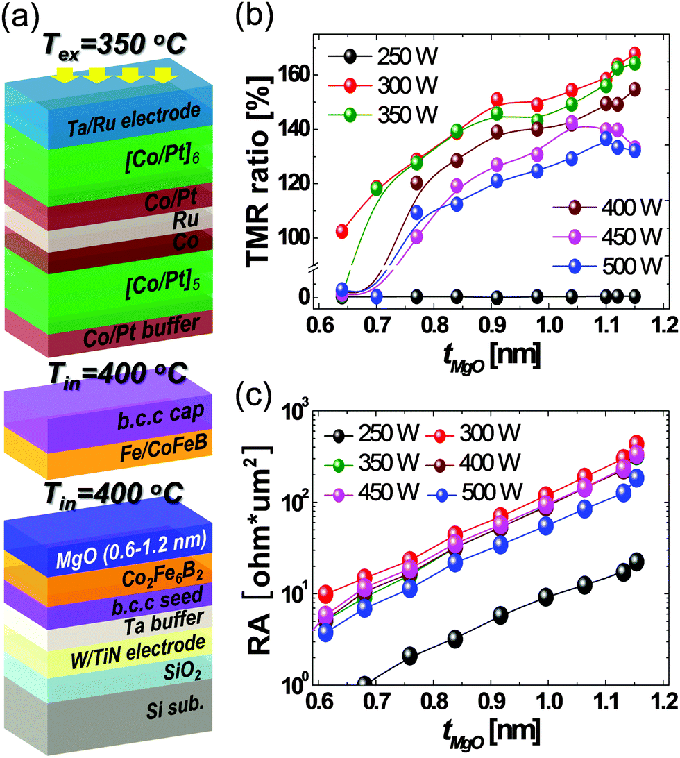 | ||
| Fig. 1 Dependency of the TMR ratio on the RF sputtering power and the MgO tunneling barrier thickness for a Co2Fe6B2/MgO based p-MTJ spin valve on 12 inch wafers: (a) schematic structure, (b) TMR ratio, (c) RA. | ||
Results and discussion
Fig. 1 shows the dependencies of the TMR ratio and RA on the tunneling barrier RF power for Co2Fe6B2–MgO based p-MTJ spin valves with [Co/Pt]n–SyAF layers. For an RF power of 400 to 500 W, the TMR ratio was almost zero (∼5%) when the tunneling barrier thickness (tMgO) was less than 0.7 nm. This indicates that the tunneling barrier's crystalline structure would be amorphous, as shown in Fig. 1(b). The TMR ratio rapidly increased and then increased approximately linearly as the tMgO was increased from 0.8 to 1.15 nm. It is particularly noteworthy that a lower tunneling barrier RF power led to higher TMR ratios; i.e., the highest TMR ratio sequence was obtained at 500, 450, and 400 W. This implies that lower RF power would lead to better tunneling crystallinity. For the RF power of 350 W, the TMR ratio at tMgO = 0.65 nm was almost zero (1.8%). The TMR ratio rapidly increased and then almost linearly increased with tMgO as tMgO was increased from 0.7 to 1.15 nm. At 350 W, the TMR ratio was higher than that at 400 W, implying that the tunneling barrier crystallinity at 350 W would be better than that at 400 W. At 300 W, the TMR ratio was 102% for tMgO = 0.65 nm and then almost linearly increased with tMgO as tMgO was increased from 0.7 to 1.15 nm. In particular, the TMR ratio was very slightly enhanced when the RF power decreased from 350 to 300 W. However, at 250 W, it abruptly dropped to almost zero (∼1.2%). In summary, the TMR ratio increased approximately linearly with tMgO at tMgO > 0.7 nm. In addition, it increased as the RF power was decreased between 300 and 500 W. The TMR ratio for all tMgO at 250 W abruptly dropped to almost zero (∼1.2%). To show the relationship between the TMR ratio and RA, Fig. 1(c) shows the dependency of RA on tMgO and the tunneling barrier RF power. For all tunneling barrier RF power values, RA exponentially increased with tMgO. Note that, in general, the tunneling barrier crystallinity improves as tMgO is increased.10,17 However, even at the same tMgO, RA increased as RF power was decreased between 300 and 500 W. Otherwise, the RA at 250 W abruptly dropped to an extremely low level. A comparison of Fig. 1(b) with (c) indicates that the dependencies of RA on tMgO and the tunneling barrier RF power are similar to those of the TMR ratio on tMgO and the tunneling barrier RF power. This implies that thicker tMgO leads to a higher RA and TMR ratio. In addition, even for the same tMgO between 300 and 500 W, lower RF power leads to a higher RA and TMR ratio.To clarify the dependencies of the TMR ratio and RA on the tunneling barrier RF power, Fig. 2(a) shows the magnetic moment vs. the magnetic field (M–H) curve and static magnetization behavior of p-MTJ spin-valves with [Co/Pt]n–SyAF layers which were scanned from 0, 15, 0, −15, and 0 kOe. In particular, to ensure the perfect PMA achievement of a [Co/Pt]n–SyAF layer, the p-MTJ spin-valves were subjected to ex situ annealing at 350 °C for 30 min under a magnetic field of 30 kOe. The perpendicular spin-electron-directions of four magnetic layers, i.e., upper [Co/Pt]6–SyAF, lower [Co/Pt]5–SyAF, CoFeB pinned, and free layer, were described, depending on the applied magnetic field. Note that a lower [Co/Pt]5–SyAF layer was ferro-magnetically coupled with the Co2Fe6B2 pinned layer, while it was anti-ferro-magnetically coupled with an upper [Co/Pt]6–SyAF layer across the Ru spacer layer, as shown in Fig. 2(a). Thus, when the applied magnetic field was scanned from 0, 500, 0, −500, and 0 Oe, only the spin-electron-direction of the Co2Fe6B2 free layers of the p-MTJ spin-valves could be rotated, as shown in Fig. 2(b)–(e).24Fig. 2(b)–(e) explain the dependency of the M–H curve and static magnetization behavior on the RF sputtering power for Co2Fe6B2 free layers of p-MTJ spin valves where the p-MTJ spin-valves were scanned from 0, 500, 0, −500, and 0 Oe. Note that the squareness amount (SQ = Mr/Ms, where Mr and Ms are respectively the remanence and saturation magnetic moment)18,19 of the M–H curve of the Co2Fe6B2 free layer achieved corresponds to the achievement of the i-PMA characteristic at the interface between the Co2Fe6B2 free layer and the MgO tunneling barrier; i.e., a higher SQ (close to 1) means a better i-PMA characteristic. For all RF power values at tMgO = 1.05 nm, the SQ of the M–H curves of the Co2Fe6B2 free layers was close to 1, indicating that the Co2Fe6B2 free layers for all RF power values achieved an excellent i-PMA characteristic, as shown in Fig. 2(a)–(d). This indicates that varying the tunneling barrier RF power did not significantly affect the Co2Fe6B2 free layer's i-PMA characteristic. Thus, the dependencies of the TMR ratio and RA on the RF power were not associated with the degradation of the Co2Fe6B2 free layer's i-PMA characteristic, which generally decreases the TMR ratio.
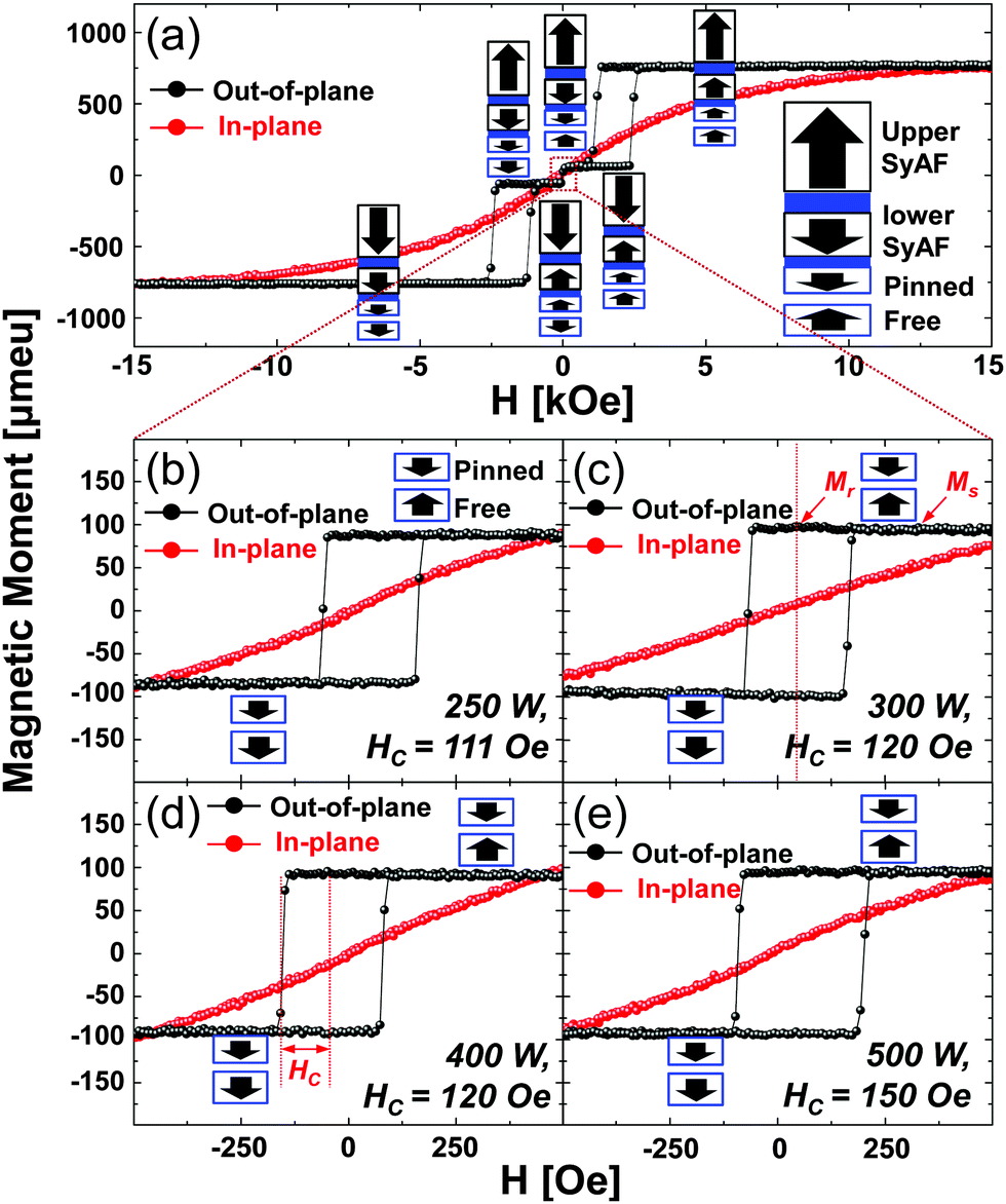 | ||
| Fig. 2 M–H curve and static magnetization behavior of p-MTJ spin-valves with a [Co/Pt]n–SyAF layer (a) and dependency of M–H curve and static magnetization behavior on the RF sputtering power for Co2Fe6B2 free layers of p-MTJ spin valves: (b) 250, (c) 300, (d) 400, (e) 500 W. | ||
In general, a decrease in the TMR ratio is mainly associated with a degraded tunneling barrier crystallinity or a degraded i-PMA characteristic at both the interface between the Co2Fe6B2 free layer and the tunneling barrier and between the Co2Fe6B2 pinned layer and the tunneling barrier.20,21 Since varying the RF power does not significantly affect the Co2Fe6B2 free layer's i-PMA characteristic (Fig. 2), we investigated the dependency of the tunneling barrier crystallinity on the RF power by high-resolution cross-sectional TEM (HR x-TEM). As mentioned previously, all p-MTJ spin valves sputtered at 250, 300, 350, 400, 450 and 500 W were subjected to in situ annealing at 400 °C for 30 min after the tunneling barrier was RF sputtered to improve the crystallinity (Fig. 1(a)). For the valve that was RF sputtered at 500 W, the targeted tunneling barrier thickness was 1.15 nm (see (a) in Fig. 3(a)). Note that the distance between the two crystalline layers in the MgO tunneling barrier is 2.01 Å.17 However, the thickness was not uniformly distributed; in Fig. 3(a), it is 1.2 nm at (a) and 0.8 nm at (b). It is particularly noteworthy that the tunneling barrier layer consists of a local mixture of an amorphous ((c) and (d) in Fig. 3(a)) and crystalline structure ((b) in Fig. 3(a)), thereby achieving a quite low TMR ratio (i.e., 132% in Fig. 1(b)). The tunneling barrier layer's amorphous structure substantially reduced the Δ1 coherent tunneling of perpendicular spin-electrons between the free and pinned Co2Fe6B2 layers; as a result, it rapidly decreased the TMR ratio of the p-MTJ spin valves.22,23 For the valve that was RF sputtered at 400 W, the tunneling barrier layer was almost completely crystallized but its thickness was not uniformly distributed; in Fig. 3(b), it is 1.0 nm at (b), 0.8 nm at (c), and 1.4 nm at (d). As shown in (a), (b), and (d), the crystal orientation of the poly-grains in the tunneling barrier layer differed from one another. A comparison of Fig. 3(a) with (b) indicates that the tunneling barrier crystallinity was obviously improved when the tunneling barrier RF power was decreased from 500 to 400 W. As a result, the TMR ratio of the p-MTJ spin valves increased from 132 to 155%. For the valve that was RF sputtered at 300 W, the tunneling barrier layer was well crystallized and its thickness was very uniformly distributed; in Fig. 3(c), it is 1.05 nm at (a)–(c). This indicates there is maximum Δ1 coherent tunneling of perpendicular spin-electrons between the free and pinned Co2Fe6B2 layers. A comparison of Fig. 3(b) with Fig. 3(c) indicates that the tunneling barrier crystallinity was evidently improved when the tunneling barrier RF power was decreased from 400 to 300 W. As a result, the TMR ratio of the p-MTJ spin valves increased from 155 to 168%. However, for the valve that was RF sputtered at 250 W, the tunneling barrier layer had an almost completely amorphous structure ((a) and (b) in Fig. 3(d)) with a locally crystallized poly grain ((c) in Fig. 3(d)). This indicates there is almost no Δ1 coherent tunneling of perpendicular spin-electrons between the free and pinned Co2Fe6B2 layers. A comparison of Fig. 3(c) with (d) indicates that the tunneling barrier crystallinity was abruptly degraded when the tunneling barrier RF power was decreased from 300 to 250 W. As a result, the TMR ratio of the p-MTJ spin valves abruptly decreased from 168 to 2%. In summary, the tunneling barrier crystallinity tended to be improved when the RF power was decreased from 500 to 300 W and tended to be abruptly degraded when it was decreased from 300 to 250 W. Thus, the TMR ratio of the p-MTJ spin valves increased as the RF power was decreased between 500 and 300 W and then abruptly decreased at less than 300 W. In addition, the dependency of the TMR ratio was well correlated with that of the tunneling barrier crystallinity on the RF power; i.e., better tunneling barrier crystallinity leads to a higher TMR ratio. In general, the compositional roughening of the MgO layer decreased with the RF sputtering power of the MgO layer so that the thickness variation of a thin (∼1.15 nm) MgO layer would decrease with the RF sputtering power, as shown by comparing Fig. 3(a)–(c) (x-TEM images for ∼1.15 nm-thick MgO layers) with the ESI† S3 (x-TEM images for ∼10 nm-thick MgO layers).† As a result, the crystallinity of a thin (∼1.15 nm) MgO layer would improve when the RF sputtering power decreases. Otherwise, a thin (∼1.15 nm) MgO layer sputtered at 250 W would be an almost amorphous MgO layer since the energy to achieve the complete crystallization of the MgO layer would not be sufficient at 250 W, as shown in Fig. 3(d) and ESI† S3(d). The detailed mechanism by which the crystallinity of ∼1.0 nm of the MgO layer depends on the MgO sputtering power is necessary for further study.
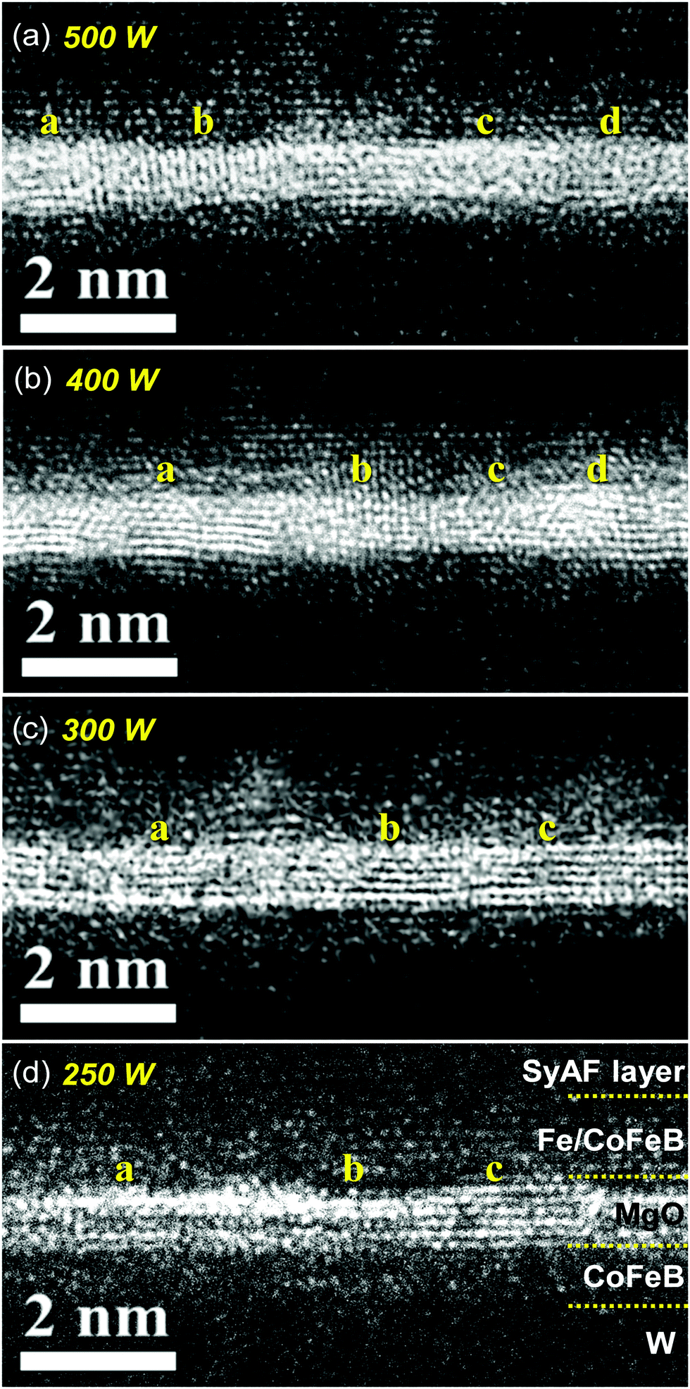 | ||
| Fig. 3 Dependency of MgO tunneling barrier crystallinity on the RF sputtering power. Targeted tunneling barrier thickness was 1.15 nm: x-TEM images for (a) 500, (b) 400, (c) 300, and (d) 250 W. | ||
Next, in order to understand the mechanism by which the TMR ratio for the p-MTJ spin valves abruptly drops to almost zero (2%) with degraded tunneling barrier crystallinity when the RF power decreases from 300 to 250 W, we investigated the optical properties of the tunneling barrier layer. They are shown as a function of the RF power in Fig. 4. The 10 nm thick MgO layers were grown on Si substrates by RF sputtering at 250 and 300 W. We first used X-ray diffraction analysis (XRD) to investigate the crystallinity of the layers. However, it was found that with this method there was no difference in full-height half-width for the (200) MgO between 250 and 300 W, indicating that XRD could not characterize the difference in the crystallinity of tunneling barriers sputtered between 250 and 300 W (see the ESI† S4). We therefore used SE to investigate the optical properties. The dielectric function (ε) is defined by ε1 + ε2, where ε1 and ε2 are the real and imaginary parts of the reflected photons at the SE detector.15 The defect state density is obtained from the imaginary part (ε2) as a function of photon energy; i.e., a higher ε2 leads to a higher defect state density due to a higher absorption of photons. The ε2 between 0 and 3.8 eV, between 3.8 and 4.3 eV, between 4.3 and 5.5 eV, and above 5.5 eV corresponds respectively to the defect state density information for Si, the interface between the Si substrate and the MgO layer, the tail state, and the conduction band state of the MgO layer. In particular, the ε2 at the interface state of the MgO layer sputtered at 250 W was higher than that sputtered at 300 W, as shown in Fig. 4(a). In addition, the ε2 at the tail state of the MgO layer sputtered at 250 W was approximately 1.5 times higher than that sputtered at 300 W. These results indicate that the defect state density at the interface between the Si substrate and the MgO layer sputtered at 250 W was higher than that sputtered at 300 W. Furthermore, the ε2 at the conduction band state of the MgO layer sputtered at 250 W was higher than that sputtered at 300 W. Next, the optical absorption coefficients (α) of the tunneling barriers sputtered at 250 and 300 W were calculated from Fig. 4(a). α is defined by α(ν) = (hν − Eg)n/hν, where Eg and hν are respectively the energy band gap of the tunneling barrier layer and the photon energy and n was 0.5 for a direct energy band-gap material such as MgO. Plotting (αhν)2vs. photon energy, we found that the energy band gaps for the MgO layer sputtered at 250 and 300 W were respectively 5.3 and 5.8 eV. We were also able to correlate the dependency of the MgO layers' optical properties on the RF power by x-TEM image observation, as shown in Fig. 4(b). For the MgO layer sputtered at 250 W, the average area of the MgO poly grains was about 9 nm2 and the grain sizes were not uniformly distributed. Since the grains had various crystal orientations, the interface between the Si substrate and the MgO layer (the ∼1.0 nm MgO layer on a Si substrate) showed poor crystallinity. However, for the MgO layer sputtered at 300 W, the average area of the poly grains was about 28 nm2 and the grain sizes were quite uniformly distributed. Thus, the interface between the Si substrate and the MgO layer (the ∼1.0 nm MgO layer on a Si substrate) showed good crystallinity. The difference in the crystallinity at the interface (the ∼1.0 nm MgO layer on a Si substrate) between 250 and 300 W (Fig. 4(b)) is well correlated with the difference in the defect state density at the interface and the MgO tail state between 250 and 300 W (Fig. 4(a)). That is, better crystallinity of a ∼1.0 nm MgO layer on a Si substrate leads to a lower defect state density at the interface and the MgO tail state. In addition, the difference in the average area of the poly grains in the tunneling barriers sputtered between 250 and 300 W is well correlated with the difference in the barriers' energy band gaps. That is, a larger poly grain area in the tunneling barrier leads to a higher energy band gap for it.25,26 Thus, optical properties such as the defect state density at the interface and the MgO tail state and the energy band gap well describe the achievement extent of good MgO layer crystallinity. In particular, the difference in the crystallinity of a ∼1.0 nm MgO layer on a Si substrate between 250 and 300 W (Fig. 4(b)) is almost directly correlated with the difference in the MgO tunneling barrier crystallinity for p-MTJ spin valves between 250 and 300 W (Fig. 3(c) and (d)). Thus, again, the abrupt decrease in the TMR ratio for p-MTJ spin valves when the RF power is reduced from 300 to 250 W is mainly associated with degraded tunneling barrier crystallinity. In addition, characterizing the optical properties of the tunneling barrier on a Si substrate by SE makes it possible to directly estimate the achievement extent of good tunneling barrier crystallinity, which forecasts decreases or increases in the TMR ratio for p-MTJ spin valves. Furthermore, in order to confirm the mechanism by which the TMR ratio for p-MTJ spin valves abruptly drops to almost zero (2%) when the RF power decreases from 300 to 250 W, we conducted X-ray reflection (XRR) measurement and simulations for the MgO tunneling barrier layers sputtered at 250 W and 300 W. The vertical structure of the MgO tunneling barrier (∼10 nm) was the same as that shown in Fig. 4(a). The roughness of the MgO layer (∼10 nm) sputtered at 250 W (∼2.11 nm) was lower than that at 300 W (∼2.47 nm), as shown in the ESI† S5, which is probably not related to the TMR ratio change. In general, a higher roughness of the MgO tunneling barrier leads to a lower TMR ratio. Otherwise, the density of the MgO layer (∼10 nm) sputtered at 250 W (5.11 g cm−3) was higher than that at 300 W (3.50 g cm−3), as shown in the ESI† S5, which is probably related to the TMR ratio change. In general, the density of the crystallized MgO layer is 3.58 g cm−3, which is similar to the density of the MgO layer sputtered at 300 W. Since the MgO tunneling barrier sputtered at 250 W was an almost amorphous layer, the density of the MgO tunneling barrier sputtered at 250 W would be higher than the well crystallized MgO tunneling barrier sputtered at 300 W. Thus, the reason that the TMR ratio for p-MTJ spin valves abruptly drops to almost zero (2%) when the RF power decreases from 300 to 250 W is associated with the density of the MgO tunneling barrier rather than the roughness (i.e., thickness variation) of the MgO tunneling barrier.
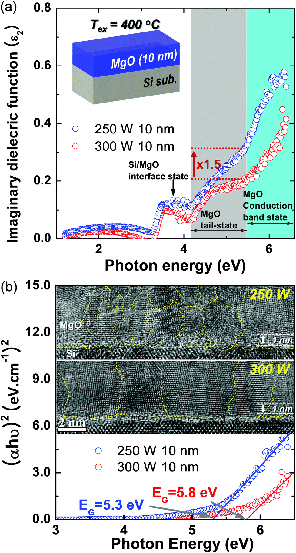 | ||
| Fig. 4 Dependency of MgO tunneling barrier optical properties on the RF sputtering power for ex situ annealing at 400 °C: (a) imaginary dielectric function vs. photon energy between 250 and 300 W and (b) correlation between x-TEM images and the tunneling barrier energy band gap analyzed by the Tauc method. | ||
Conclusions
Our study results showed that for Co2Fe6B2–MgO-based p-MTJ spin valves with [Co/Pt]n–SyAF layers, the tunneling magneto-resistance (TMR) ratio and resistance-area product (RA) strongly depended on the radio-frequency (RF) sputtering power (“RF power”) of the MgO tunneling barrier. The TMR ratio and RA increased rapidly and approximately linearly as the RF power was decreased between 300 and 500 W and abruptly dropped at 250 W. Thus, the TMR ratio peaked at a specific RF power; i.e., 168% for a 1.15 nm thick tunneling barrier at 300 W. The dependency of the TMR ratio and RA on the RF power was mainly associated with the tunneling barrier's face-centered-cubic crystallinity. Better crystallinity led to a higher TMR ratio and RA. The crystallinity was strongly dependent on the RF power; i.e., it became better when the RF power was decreased from 500 to 300 W and then rapidly degraded at 250 W. Thus, the dependency of the TMR ratio and RA on the RF power was well correlated with that of the tunneling barrier crystallinity on the RF power. However, it was found that varying the RF power did not significantly affect the interfacial-perpendicular magnetic anisotropy (i-PMA) characteristics in the free and pinned Co2Fe6B2 layers. Furthermore, the crystallinity of a ∼1.0 nm tunneling barrier observed by x-TEM was well correlated with optical properties such as the energy band gap and the defect state densities at the interface and the tail state of the MgO layer measured by spectroscopic ellipsometry (SE). A higher energy band gap and lower defect state densities led to better MgO layer crystallinity. In particular, since a higher energy band gap in the MgO layer corresponded to larger poly-grain size in the layer at the same layer thickness, designing the RF power to achieve larger tunneling barrier grain size would appear to be a key engineering issue for achieving a higher TMR ratio and lower RA in Co2Fe6B2–MgO-based p-MTJ spin valves. In addition, since the optical properties measured by spectroscopic SE well described the crystallinity of the ∼1.0 nm MgO layer, SE can be considered an essential non-destructive tool for in-line monitoring of tunneling barrier quality on a 12 inch wafer.Acknowledgements
This work was supported by the Basic Science Research Program through the National Research Foundation of Korea (NRF) grant funded by the Korea government (MSIP) (No. 2014R1A2A1A01006474) and the Brain Korea 21 PLUS Program in 2014.Notes and references
- K. C. Chun, H. Zhao, J. D. Harms, T.-H. Kim, J.-P. Wang and C. H. Kim, IEEE J. Solid-State Circuits, 2013, 48, 598–610 CrossRef.
- S. A. Wolf, D. D. Awschalom, R. A. Buhrman, J. M. Daughton, S. von Molnar, M. L. Roukes, A. Y. Chtchelkanova and D. M. Treger, Science, 2001, 294, 1488–1495 CrossRef CAS PubMed.
- J. G. Park, T. H. Shim, K. S. Chae, D. Y. Lee, Y. Takemura, S. E. Lee, M. S. Jeon, J. U. Baek, S. O. Park and J. P. Hong, International Electron Devices Meeting, San Francisco, CA, 2014, p. 19.2.1 Search PubMed.
- W. Kim, J. Y. Jeong, Y. Kim, W. C. Lim, J. H. Kim, j. H. Park, H. J. Shin, Y. S. Park, K. S. Kim, S. H. Park, Y. J. Lee, W. Kim, H. J. Kwon, H. L. Park, H. S. Ahn, S. C. Oh, J. E. Lee, S. O. Park, S. Choi, H. K. Kang and C. Chung, International Electron Devices Meeting, Washington, DC, 2011, p. 24.1.1 Search PubMed.
- S. Ikeda, K. Miura, H. Yamamoto, K. Mizunuma, H. D. Gan, M. Endo, S. Kanai, J. Hayakawa, F. Matsukura and H. Ohno, Nat. Mater., 2010, 9, 721–724 CrossRef CAS PubMed.
- D. D. Lam, F. Bonell, S. Miwa, Y. Shiota, K. Yakushiji, H. Kubota, T. Nozaki, A. Fukushima, S. Yuasa and Y. Suzuki, J. Korean Phys. Soc., 2013, 62, 1461–1464 CrossRef CAS.
- H. Ohmori, T. Hatori and S. Nakagawa, J. Appl. Phys., 2008, 103, 07A911 CrossRef.
- T. Urano and T. Kanaji, J. Phys. Soc. Jpn., 1988, 57, 3403–3410 CrossRef CAS.
- A. Manchon, C. Ducruet, L. Lombard, S. Auffret, B. Rodmacq, B. Dieny, S. Pizzini, J. Vogel, V. Uhliř, M. Hochstrasser and G. Panaccione, J. Appl. Phys., 2008, 104, 043914 CrossRef.
- K. Nakamura, T. Akiyama, T. Ito, M. Weinert and A. J. Freeman, Phys. Rev. B: Condens. Matter Mater. Phys., 2010, 81, 220409 CrossRef.
- B. Rodmacq, A. Manchon, C. Ducruet, S. Auffret and B. Dieny, Phys. Rev. B: Condens. Matter Mater. Phys., 2009, 79, 024423 CrossRef.
- H. X. Yang, M. Chshiev, B. Dieny, J. H. Lee, A. Manchon and K. H. Shin, Phys. Rev. B: Condens. Matter Mater. Phys., 2011, 84, 054401 CrossRef.
- K. Yamane, Y. Higo, H. Uchida, N. Yuji, S. Sasaki, H. Ohmori, K. Bessho and M. Hosomi, IEEE Trans. Magn., 2013, 49, 4335–4338 CrossRef CAS.
- D. C. Worledge and P. L. Trouilloud, Appl. Phys. Lett., 2003, 83, 84 CrossRef CAS.
- Y.-X. Zheng, R.-J. Zhang and L.-Y. Chen, Stoichiom. Mater. Sci.: When Numbers Matter, 2012, 3, 49–82 Search PubMed.
- M. Kurth, P. C. J. Graat and E. J. Mittemeijer, Thin Solid Films, 2006, 500, 61–69 CrossRef CAS.
- S. Yuasa and D. D. Djayaprawira, J. Phys. D: Appl. Phys., 2007, 40, R337–R354 CrossRef CAS.
- C.-W. Cheng, W. Feng, G. Chern, C. M. Lee and T. h Wu, J. Appl. Phys., 2011, 110, 033916 CrossRef.
- M. Ciureanu, F. Beron, L. Clime, P. Ciureanu, A. Yelon, T. A. Ovari, R. W. Cochrane, F. Normandin and T. Veres, Electrochim. Acta, 2005, 50, 4487–4497 CrossRef CAS.
- D.-Y. Lee, T.-H. Shim and J.-G. Park, Appl. Phys. Lett., 2013, 102, 212409 CrossRef.
- N. Miyakawa, D. C. Worledge and K. Kita, IEEE Magn. Lett., 2013, 4, 1000104 CrossRef.
- A. V. Khvalkovskiy, D. Apalkov, S. Watts, R. Chepulskii, R. S. Beach, A. Ong, X. Tang, A. Driskill-Smith, W. H. Butler, P. B. Visscher, D. Lottis, E. Chen, V. Nikitin and M. Krounbi, J. Phys. D: Appl. Phys., 2013, 46, 074001 CrossRef.
- W. Butler, X. Zhang, T. Schulthess and J. MacLaren, Phys. Rev. B: Condens. Matter Mater. Phys., 2001, 63, 054416 CrossRef.
- M.-S. Lin and C.-H. Lai, J. Appl. Phys., 2007, 101, 09D121 Search PubMed.
- N. Badar, N. F. Chayed, R. Rusdi, N. Kamarudin and N. Kamarulzaman, Adv. Mater. Res., 2012, 545, 157–160 CrossRef CAS.
- A. Kumar and J. Kumar, J. Phys. Chem. Solids, 2008, 69, 2764 CrossRef CAS.
- K. S. Chae and J. G. Park, J. Appl. Phys., 2015, 117, 153901 CrossRef.
Footnote |
| † Electronic supplementary information (ESI) available. See DOI: 10.1039/c5tc03669k |
| This journal is © The Royal Society of Chemistry 2016 |