
Highly efficient terbium(III)-based organic light-emitting diodes obtained by exciton confinement†
Gang
Yu
a,
Fei
Ding
a,
Huibio
Wei
a,
Zifeng
Zhao
a,
Zhiwei
Liu
a,
Zuqiang
Bian
*a,
Lixin
Xiao
b and
Chunhui
Huang
a
aBeijing National Laboratory for Molecular Sciences, State Key Laboratory of Rare Earth Materials Chemistry and Applications, College of Chemistry and Molecular Engineering, Peking University, Beijing, 100871, China. E-mail: bianzq@pku.edu.cn
bState Key Laboratory for Mesoscopic Physics, Department of Physics, Peking University, Beijing 100871, China
First published on 16th November 2015
Abstract
We present highly efficient Tb(III)-based organic light-emitting diodes optimized by the subtle choice of bipolar hosts, adjacent layers and double emitting structures. By introducing di(9H-carbazol-9-yl)(phenyl)phosphine oxide (DCPPO) as the host for the first emitting layer, and 9-(4-tert-butylphenyl)-3,6-bis(diphenylphosphine oxide)-carbazole (DPPOC) for the second emitting layer for Tb(PMIP)3 (PMIP stands for 1-phenyl-3-methyl-4-isobutyryl-pyrazol-5-one), the excitons can be well confined within the double-emitting layer. When 4,4′,4′′-tris(N-carbazolyl)triphenylamine (TCTA) and tris-[3-(3-pyridyl)mesityl]borane (3TPYMB) with high triplet energy levels are used as a hole transporting layer (HTL) and an electron transporting layer (ETL), respectively, the optimized device reaches a maximum efficiency of 52 lm W−1, 57 cd A−1, i.e. a maximum external quantum efficiency (EQE) of 15%. At a practical brightness of 100 cd m−2 (4.6 V) the efficiency remains at around 20 lm W−1, 30 cd A−1.
Introduction
Although organic light-emitting diodes (OLEDs) have been commercialized as flat panel displays since 1997, only singlet excitons were emitted. To achieve 100% of internal quantum efficiency (IQE), i.e., the full use of singlet and triplet excitons, phosphorescence OLEDs (PhOLEDs)1,2 and thermally activated delayed fluorescence (TADF)3,4 have attracted increasing attention. However, it is still a challenge to achieve a high color purity with 100% IQE. Lanthanide complexes are also candidates for the full use of both singlet and triplet excitons.5–22 Lanthanide ions are excited via intramolecular energy transfer from the triplet excited states of the ligands in lanthanide complexes, and the relaxation from the singlet to the triplet states of the ligands also occurs through intersystem crossing. Hence the energy of both singlet and triplet excitons formed by electron–hole recombination can be utilized for emission with a 100% theoretical emission quantum efficiency.6,23–31 In addition, in contrast to other organic chromophores, lanthanide ions can exhibit spectrally narrow emission due to intra-atomic transitions within the 4f shell, as known from inorganic luminescent materials in cathode-ray tubes. Some reported work also made use of the particularity of certain lanthanide complexes for special dopants or circularly polarized electroluminescence.32,33Since 1990, a number of studies based on Tb(III)-based OLEDs have been reported. The maximum luminance has been improved from 7 cd m−2![[thin space (1/6-em)]](https://www.rsc.org/images/entities/char_2009.gif) 23 to more than 2000 cd m−2,34,35 and the maximum efficiency has risen to 36 cd A−1, 16 lm W−1. At a practical brightness of 100 cd m−2, the best efficiency was 15.7 cd A−1.35
23 to more than 2000 cd m−2,34,35 and the maximum efficiency has risen to 36 cd A−1, 16 lm W−1. At a practical brightness of 100 cd m−2, the best efficiency was 15.7 cd A−1.35
In the reported work,35 pure Tb(PMIP)3 (PMIP stands for 1-phenyl-3-methyl-4-isobutyryl-pyrazol-5-one) acting as the first emitting layer in the device was demonstrated to be most important for the green electroluminescence with the high efficiency. Without the first Tb(PMIP)3 layer, the emission of NPB (N,N′-diphenyl-N,N′-bis(1-naphthyl)-1,10-diphenyl-4,4′-diamine) was observable at high current density while the mono-emitting layer is as thick as 60 nm in the device ITO/NPB/Tb(PMIP)3(DPPOC) (DPPOC stands for 9-(4-tert-butylphenyl)-3,6-bis(diphenylphosphine oxide)-carbazole)/BCP (2,9-dimethyl-4,7-diphenyl-1,10-phenanthroline)/Alq3 (tris(8-hydroxyquinoline))/Mg0.9Ag0.1. When pure Tb(PMIP)3 was introduced between the hole-transporting layer (HTL) and the emitting layer (EML), a thickness of 20 nm was required to completely eliminate the emission from NPB in the device ITO/NPB/Tb(PMIP)3/Tb(PMIP)3(DPPOC)/BCP/Alq3/Mg0.9Ag0.1.
Now, we have further improved the electroluminescence (EL) efficiency based on triplet confinement by the subtle choice of adjacent layers, balancing the carrier transport by using a new first emitting layer. When 4,4′,4′′-tris(N-carbazolyl)triphenylamine (TCTA) and tris-[3-(3-pyridyl)mesityl]borane (3TPYMB) with high triplet energy levels are used as a HTL and an electron transporting layer (ETL), respectively, the device ITO/MoO3 (1 nm)/TCTA:MoO3 (20%) (20 nm)/TCTA (15 nm)/Tb(PMIP)3:DCPPO (dicarbazolylphenylphosphine) (1:1) (10 nm)/Tb(PMIP)3:DPPOC (1:1) (10 nm)/3TPYMB (50 nm)/LiF (1 nm)/Al (100 nm) reaches a maximum efficiency of 52 lm W−1, 57 cd A−1, i.e. a maximum external quantum efficiency (EQE) of 15%. At a practical brightness of 100 cd m−2 (4.6 V) the efficiency remains at around 20 lm W−1, 30 cd A−1, which renews a record for Tb(III)-based OLEDs.
Experimental section
Materials
MoO3, NPB, Alq3 (tris(8-hydroxyquinoline) aluminum), TCTA (4,4′,4′′-tris(N-carbazolyl)triphenylamine), TPBi (1,3,5-tris(N-phenylbenzimidazole-2-yl)benzene) and 3TPYMB (tris-[3-(3-pyridyl)mesityl]borane) were purchased from Lumtec Tech. Corp. Tb(PMIP)3 and DPPOC were synthesized as in our previous report.35 DCPPO was synthesized as in ref. 36.Device fabrication and testing
The indium tin oxide (ITO) patterned anode was commercially available with a sheet resistance of 14 Ω square−1. Before loading into a deposition chamber, the ITO substrate was cleaned with deionized water and organic solvents, and finally treated with ultraviolet (UV) ozone. The organic and metal layers were deposited in different vacuum chambers with a base pressure better than 8 × 10⁻⁵ Pa. The active area for all devices was 4 mm2. All electric testing and optical measurements were performed under ambient conditions without encapsulation. The EL spectra were measured using a Spectra Scan PR650. The current–voltage (I–V) and luminance–voltage (L–V) characteristics were measured using a computer controlled Keithley 2400 Sourcemeter unit with a calibrated silicon diode.The materials are listed in Scheme 1. The device structures are listed as follows:
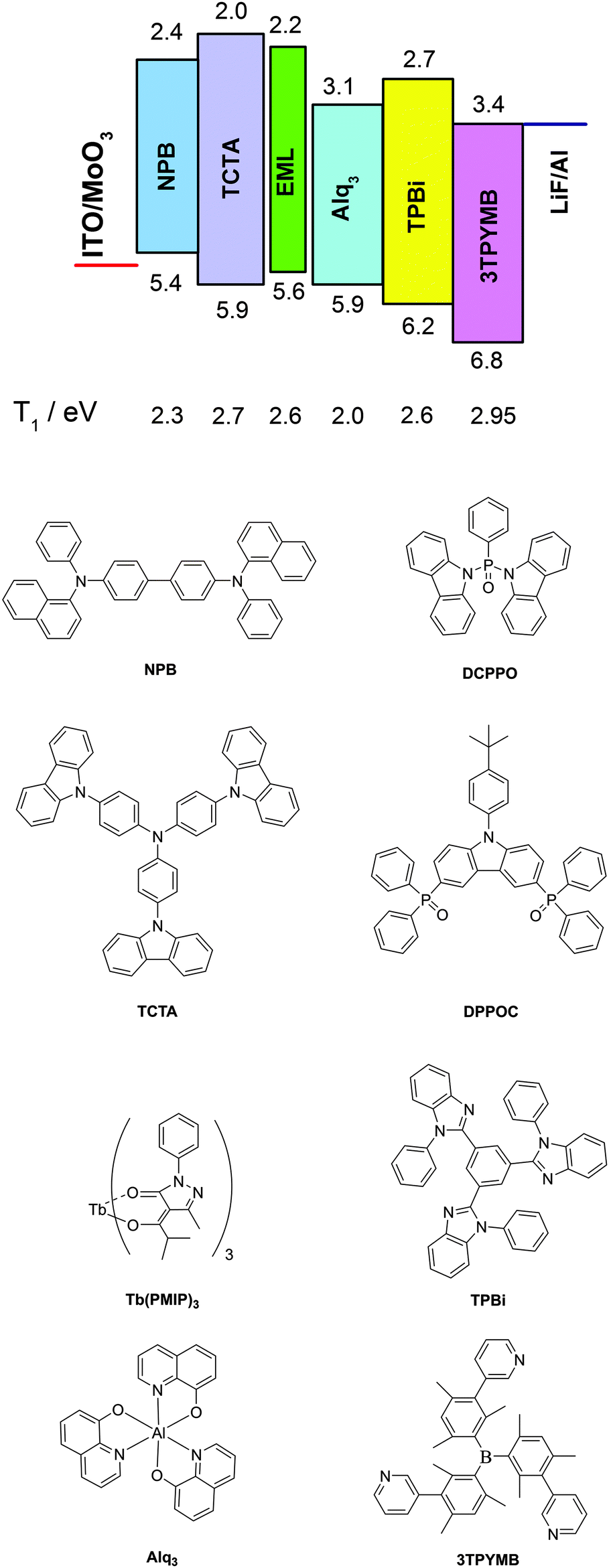 | ||
| Scheme 1 OLED device structure and the molecular structures of the compounds used in these devices. | ||
Device A: ITO/MoO3 (1 nm)/NPB (35 nm)/Tb(PMIP)3:DPPOC (1:1) (20 nm)/Alq3 (40 nm)/LiF (1 nm)/Al (100 nm)
Device B: ITO/MoO3 (1 nm)/TCTA (35 nm)/Tb(PMIP)3:DPPOC (1:1) (20 nm)/TPBi (40 nm)/LiF (1 nm)/Al (100 nm)
Device C: ITO/MoO3 (1 nm)/TCTA (35 nm)/Tb(PMIP)3:DPPOC (1:1) (20 nm)/3TPYMB (40 nm)/LiF (1 nm)/Al (100 nm)
Device D: ITO/MoO3 (1 nm)/TCTA (35 nm)/Tb(PMIP)3:DCPPO (1:1) (10 nm)/Tb(PMIP)3:DPPOC (1:1) (10 nm)/3TPYMB (40 nm)/LiF (1 nm)/Al (100 nm)
Device E: ITO/MoO3 (1 nm)/TCTA:MoO3 (20%) (20 nm)/TCTA (15 nm)/Tb(PMIP)3:DCPPO (1:1) (10 nm)/Tb(PMIP)3:DPPOC (1:1) (10 nm)/3TPYMB (50 nm)/LiF (1 nm)/Al (100 nm)
Results and discussion
In order to facilitate comparison with the previous work,35 we firstly fabricated device A, ITO/MoO3 (1 nm)/NPB (35 nm)/Tb(PMIP)3:DPPOC (1:1) (20 nm)/Alq3 (40 nm)/LiF (1 nm)/Al (100 nm), with traditional materials NPB as the HTL and Alq3 as the ETL, respectively. The EL performance is shown in Fig. 2 and Table 1. The device showed a relatively high turn-on voltage of 4.7 V, identical to the previous report.35 From the EL spectra, emission of NPB at 450 nm was observable even at low luminance, and became more intense as the driving voltage increased, which shows an apparent exciton “loss” to NPB. Then the CIE coordinate at 100 cd m−2 was (0.27, 0.51), which was located in the blue-green zone, significantly reducing the color purity. The maximum external quantum efficiency barely reached 3%. This low efficiency results mainly from two factors. The first one is imbalanced carrier mobility. DPPOC has two phenylphosphine oxide groups, which makes it a potential electron transporting material and results in the exciton recombination area near the HTL especially at high current density. The second one is triplet energy dissipation to adjacent layers, considering NPB's relatively low T1 of 2.3 eV,37 which can be transferred from the excited state of PMIP. A simple strategy of adding a layer of pure Tb(PMIP)3 was proposed to block NPB emission by us as-mentioned in the Introduction part.
| V on [V] | V 100 [V] | L max [cd m−2] | LEmax [cd A−1] | LE100 [cd A−1] | EQEmax [%]c | EQE100 [%]c | EQE500 [%]d | PEmax [lm W−1] | PE100 [lm W−1] | CIE100 [x, y] | |
|---|---|---|---|---|---|---|---|---|---|---|---|
| a At 100 cd m−2. b Corresponding driving voltage is listed in the bracket. c Calculated using Matlab according to the emission spectra and current-luminance relativity. d At 500 cd m−2. | |||||||||||
| A | 4.7 | 7.9 | 3823 (17) | 7.9 | 5.6 | 2.6 | 1.9 | 1.5 | 5.0 | 2.2 | 0.27, 0.51 |
| B | 3.8 | 5.3 | 2592 (14) | 32 | 23 | 8.2 | 6.3 | 3.4 | 25 | 13 | 0.30, 0.62 |
| C | 4.0 | 6.6 | 1672 (14) | 44 | 25 | 11.6 | 6.6 | 2.9 | 35 | 12 | 0.32, 0.62 |
| D | 4.1 | 6.4 | 2438 (15) | 48 | 28 | 12.5 | 7.4 | 3.4 | 34 | 14 | 0.31, 0.62 |
| E | 3.4 | 4.6 | 2784 (10) | 57 | 30 | 14.8 | 7.7 | 3.2 | 52 | 20 | 0.32, 0.62 |
To root out the emission of NPB, the HTL was replaced with TCTA (T1 = 2.7 eV)38 for the remaining improved devices, and an alternative ETL was chosen from TPBi and 3TPYMB with higher T1 values of 2.6 eV39 and 2.95 eV,40 respectively. Device B with TPBi displayed a dramatic efficiency rise compared to device A with a four-fold maximum luminous efficiency and five-fold maximum power efficiency. Pure Tb(III) emission was realized at practical brightness with the efficiency of 23 cd A−1, 13 lm W−1. This could be mainly attributed to TCTA and TPBi's higher T1 than NPB and Alq3 (2.0 eV),39 respectively. In lanthanide complex electroluminescence, the S1 state of the ligand transferred to the triplet energy levels through intersystem crossing, and then to the excited state of the Ln ions and released as f–f relaxation. In some cases, higher energy levels may be excited by the ligand but nonradiative relaxations occur from these higher energy levels until the energy has decayed to the emitting levels where visible radiation originates.41 Triplet confinement can be a crucial factor when generated excitons' energy was transferring to the central Ln ions. If adjacent layers had lower T1 levels, the energy could transfer to the adjacent layers and relax as non-radiative transition (Fig. 1). Due to better electron mobility and suitable LUMO levels, device B showed a lower turn-on voltage of 3.8 V and a faster current rise (Fig. 2a). To be noted, the LUMO level of TCTA is 0.2 eV higher than NPB, which can block some electron when compared to NPB. This is a positive effect for avoiding exciton recombination in the HTL, and indeed no emission of the HTL was found at practical luminance. However, these devices all showed large efficiency roll-off especially at high luminance (Table 1). This efficiency roll-off is probably caused by the long luminescence lifetime of Tb(PMIP)3. The luminescence lifetime of co-deposited film of Tb(PMIP)3:DPPOC (1:1) was as long as 764 μs (Fig. S2, ESI†). Two quenching mechanisms of triplet–triplet and polaron–triplet annihilation are suggested to be the main negative effect.42
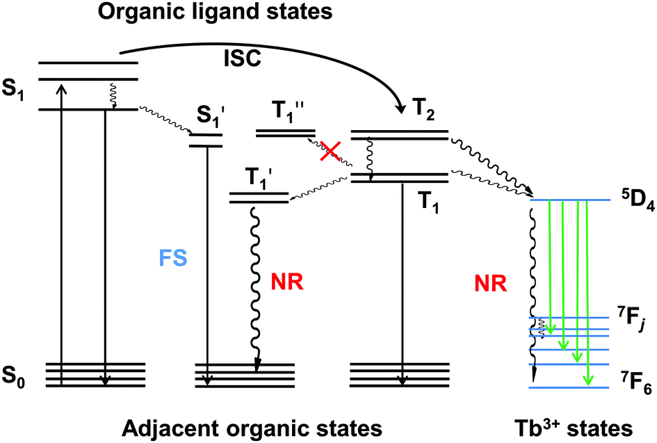 | ||
| Fig. 1 Energy transfer in lanthanide luminescence: FS = fluorescence; NR = nonradiative decay. S1 and T1 stand for the energy levels of PMIP; S1′, T1′ and T1′′ stand for the energy levels of different adjacent layers. | ||
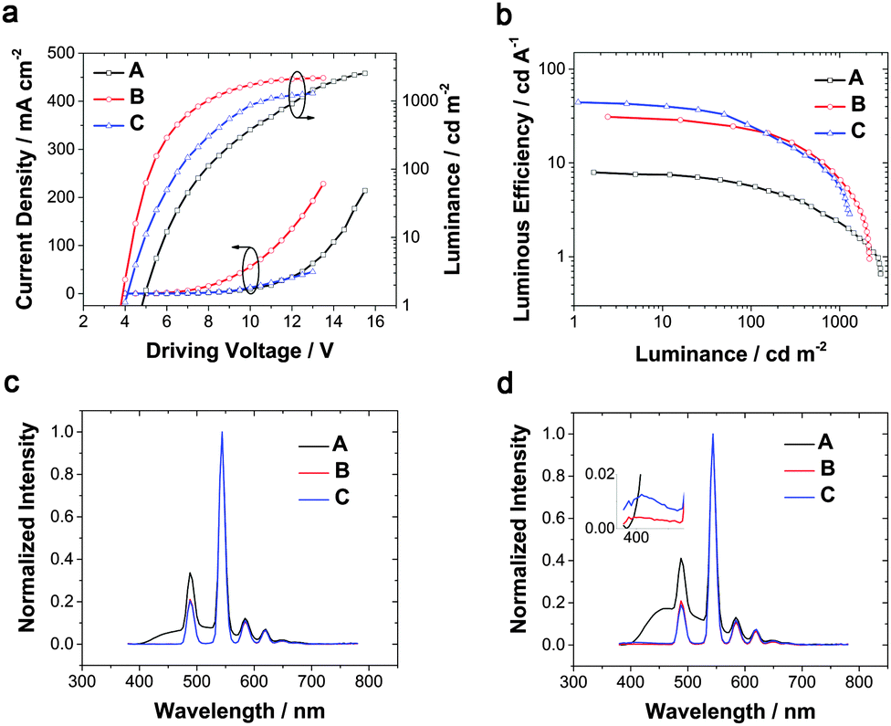 | ||
| Fig. 2 EL performance of devices A–C. Current density–voltage–brightness characteristics (a), luminous efficiency-luminance curves (b) and EL spectra of devices A–C on luminance at around 100 cd m−2 (c) and 1000 cd m−2 (d). | ||
Since TPBi's T1 is almost equivalent to the 5D4 level of Tb(III), not high enough to efficiently avoid energy dissipation, 3TPYMB with T1 as high as 2.95 eV was introduced as the ETL to fabricate device C. The maximum efficiency could reach 44 cd A−1. The turn-on voltage rose a little to 4.0 V, and 6.6 V was required to reach 100 cd m−2, which could be ascribed to 3TPYMB's deeper LUMO and lower electron-mobility than TPBi.39
When TCTA acted as the HTL, pure green emission of Tb(III) with the CIE coordinates of (0.32, 0.62) was realized at a few hundred cd m−2, but a small peak at around 400 nm rose at high luminance (Fig. 2d), which can be assigned to emission from TCTA.43 The intensity of the TCTA peak at high luminance can reveal the location of the exciton recombination area, corresponding to the NPB emission in device A. DPPOC with two DPPO groups increases the electron-mobility of the emitting layer, resulting in the recombination zone near the interface between the HTL and the EML (Fig. 3a). Therefore, another host dicarbazolylphenylphosphine oxide (DCPPO) with two carbazole groups was introduced in a double-emitting-layer device D, ITO/MoO3 (1 nm)/TCTA (35 nm)/Tb(PMIP)3:DCPPO (1:1) (10 nm)/Tb(PMIP)3:DPPOC (1:1) (10 nm)/3TPYMB (40 nm)/LiF (1 nm)/Al (100 nm). DCPPO has a high T1 of 3.0 eV,36 high enough to transfer to Tb(PMIP)3. Pure characteristic emission of Tb(III) can be realized (Fig. 4c and Fig. S1, ESI†). The EL performance of device C–E are shown in Fig. 4. The TCTA emission at high luminance was almost eliminated in device D, which revealed that the excitons were well-confined within the EML (Fig. 3b and 4d) due to the hole-transporting ability of the first EML. As a result, device D showed a maximum efficiency of 48 cd A−1, 34 lm W−1. We successfully controlled the charge balance and exciton recombination by bipolar host and adjacent materials.44 With the p-doped TCTA layer (TCTA:MoO3, 20 wt%) and thickness modification of 3TPYMB, device E showed a turn-on voltage as low as 3.4 V, a faster current rise, a maximum efficiency of 57 cd A−1, 52 lm W−1 and an EQE of 15%. The relative lower driving voltage and faster current rise could mainly be attributed to the better carrier mobility of p-doped TCTA. Even at a luminance of 100 cd m−2, the efficiency remained at 30 cd A−1, 20 lm W−1, which is the best result of Tb(III)-complex electroluminescence reported so far. We also tested the lifetime of device E. Unfortunately, the LT50 of device E at an initial luminance of 800 cd m−2 is only 19.1 minutes (Fig. S3, ESI†). This can be translated to a LT50 at 100 cd m−2 of only 10.8 h using the formula LT50(L1) = LT50(L0)*(L0/L1)1.7.45 The instability of the β-diketonate ligand could be the main reason for the short lifetime of the device.46–48 Further exploration of stable ligands for lanthanide luminescent complexes is under progress in our group.
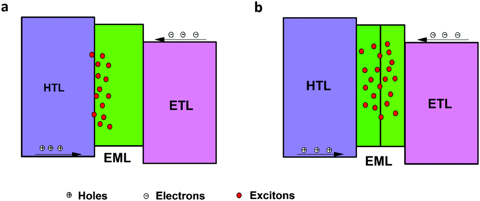 | ||
| Fig. 3 Exciton recombination zone at high luminance of the single-emitting structure (a) and double-emitting structure (b). | ||
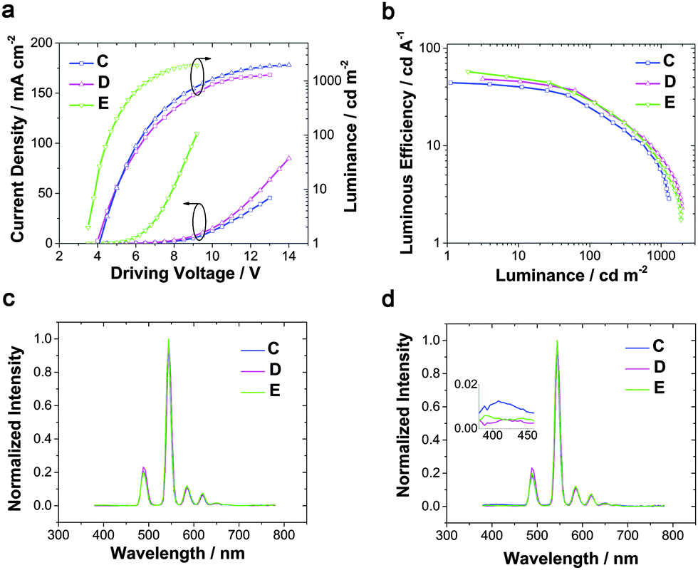 | ||
| Fig. 4 EL performance of devices C–E. Current density–voltage–brightness characteristics (a), luminous efficiency-luminance curves (b) and EL spectra of devices C–E on luminance at around 100 cd m−2 (c) and 1000 cd m−2 (d). | ||
Conclusions
A series of devices based on Tb(PMIP)3 employing different charge-transporting layers and different emitting-layers were fabricated. The device efficiency had a positive correlation with the lowest triplet energy of both adjacent layers. After a bipolar host with more carbazole groups and a double-emitting layer structure was introduced, the device performance was further optimized to a maximum EQE of 15%. At 100 cd m−2, the efficiency was 30 cd A−1 and 20 lm W−1 at a driving voltage of 4.6 V. This work renews the record of the EL performance of Tb(III)-based devices and indicates the potential of application of Tb(III)-based OLEDs in future flat-display area.Conflicts of interest
The authors declare no competing financial interest.Acknowledgements
The financial support of the National Basic Research Program (2014CB643800) and NNSFC (21321001, 21371012) is gratefully acknowledged.Notes and references
- M. A. Baldo, M. E. Thompson and S. R. Forrest, Nature, 2000, 403, 750–753 CrossRef CAS PubMed.
- L. X. Xiao, S. J. Su, Y. Agata, H. L. Lan and J. Kido, Adv. Mater., 2009, 21, 1271–1274 CrossRef CAS.
- H. Uoyama, K. Goushi, K. Shizu, H. Nomura and C. Adachi, Nature, 2012, 492, 234–238 CrossRef CAS PubMed.
- Q. Zhang, B. Li, S. Huang, H. Nomura, H. Tanaka and C. Adachi, Nat. Photonics, 2014, 8, 326–332 CrossRef CAS.
- J. Kido and Y. Okamoto, Chem. Rev., 2002, 102, 2357–2368 CrossRef CAS PubMed.
- J. Kalinowski, Opt. Mater., 2008, 30, 792–799 CrossRef CAS.
- S. V. Eliseeva and J. C. Bunzli, Chem. Soc. Rev., 2010, 39, 189–227 RSC.
- C. Adachi, M. A. Baldo and S. R. Forrest, J. Appl. Phys., 2000, 87, 8049 CrossRef CAS.
- C. J. Liang, D. Zhao, Z. R. Hong, D. X. Zhao, X. Y. Liu, W. L. Li, J. B. Peng, J. Q. Yu, C. S. Lee and S. T. Lee, Appl. Phys. Lett., 2000, 76, 67–69 CrossRef CAS.
- Z. R. Hong, C. J. Liang, R. G. Li, W. L. Li, D. Zhao, D. Fan, D. Y. Wang, B. Chu, F. X. Zang, L. S. Hong and S. T. Lee, Adv. Mater., 2001, 13, 1241–1245 CrossRef CAS.
- F. Liang, Q. Zhou, Y. Cheng, L. Wang, D. Ma, X. Jing and F. Wang, Chem. Mater., 2003, 15, 1935–1937 CrossRef CAS.
- P. P. Sun, J. P. Duan, J. J. Lih and C. H. Cheng, Adv. Funct. Mater., 2003, 13, 683–691 CrossRef CAS.
- H. Xu, L. H. Wang, X. H. Zhu, K. Yin, G. Y. Zhong, X. Y. Hou and W. Huang, J. Phys. Chem. B, 2006, 110, 3023–3029 CrossRef CAS PubMed.
- X. C. Gao, H. Cao, C. H. Huang, B. G. Li and S. Umitani, Appl. Phys. Lett., 1998, 72, 2217–2219 CrossRef CAS.
- X. C. Gao, H. Cao, C. H. Huang, S. Umitani, G. Q. Chen and P. Jiang, Synth. Met., 1999, 99, 127–132 CrossRef CAS.
- V. Christou, O. V. Salata, T. Q. Ly, S. Capecchi, N. J. Bailey, A. Cowley and A. M. Chippindale, Synth. Met., 2000, 111, 7–10 CrossRef.
- J. Wang, R. Wang, J. Yang, Z. Zheng, M. D. Carducci, T. Cayou, N. Peyghambarian and G. E. Jabbour, J. Am. Chem. Soc., 2001, 123, 6179–6180 CrossRef CAS PubMed.
- S. Eliseeva, O. Kotova, O. Mirzov, K. Anikin, L. Lepnev, E. Perevedentseva, A. Vitukhnovsky and N. Kuzmina, Synth. Met., 2004, 141, 225–230 CrossRef CAS.
- H. Xin, M. Shi, X. C. Gao, Y. Y. Huang, Z. L. Gong, D. B. Nie, H. Cao, Z. Q. Bian, F. Y. Li and C. H. Huang, J. Phys. Chem. B, 2004, 108, 10796–10800 CrossRef CAS.
- P. P. Lima, F. A. A. Paz, C. D. S. Brites, W. G. Quirino, C. Legnani, M. Costa e Silva, R. A. S. Ferreira, S. A. Júnior, O. L. Malta, M. Cremona and L. D. Carlos, Org. Electron., 2014, 15, 798–808 CrossRef CAS.
- J. Wang, C. Han, G. Xie, Y. Wei, Q. Xue, P. Yan and H. Xu, Chem. – Eur. J., 2014, 20, 11137–11148 CrossRef CAS PubMed.
- H. Xu, J. Z. Wang, Y. Wei, G. H. Xie, Q. Xue, Z. P. Deng and W. Huang, J. Mater. Chem. C, 2015, 3, 1893–1903 RSC.
- J. Kido, K. Nagai and Y. Ohashi, Chem. Lett., 1990, 657–660 CrossRef CAS.
- J. Kido, H. Hayase, K. Hongawa, K. Nagai and K. Okuyama, Appl. Phys. Lett., 1994, 65, 2124–2126 CrossRef CAS.
- A. Edwards, C. Claude, I. Sokolik, T. Y. Chu, Y. Okamoto and R. Dorsinville, J. Appl. Phys., 1997, 82, 1841–1846 CrossRef CAS.
- J. Kalinowski, W. Stampor, M. Cocchi, D. Virgili and V. Fattori, Appl. Phys. Lett., 2005, 86, 241106 CrossRef.
- T. Oyamada, Y. Kawamura, T. Koyama, H. Sasabe and C. Adachi, Adv. Mater., 2004, 16, 1082–1086 CrossRef CAS.
- H. Xin, F. Y. Li, M. Shi, Z. Q. Bian and C. H. Huang, J. Am. Chem. Soc., 2003, 125, 7166–7167 CrossRef CAS PubMed.
- M. Sun, H. Xin, K. Z. Wang, Y. A. Zhang, L. P. Jin and C. H. Huang, Chem. Commun., 2003, 702–703, 10.1039/b212467j.
- M. Guan, Z. Qiang Bian, F. You Li, H. Xin and C. Hui Huang, New J. Chem., 2003, 27, 1731 RSC.
- Z. Chen, F. Ding, F. Hao, M. Guan, Z. Bian, B. Ding and C. Huang, New J. Chem., 2010, 34, 487 RSC.
- L. Zhou, L. Li, Y. Jiang, R. Cui, Y. Li, X. Zhao and H. Zhang, ACS Appl. Mater. Interfaces, 2015, 7, 16046–16053 CAS.
- F. Zinna, U. Giovanella and L. Di Bari, Adv. Mater., 2015, 27, 1791–1795 CrossRef CAS PubMed.
- S. Capecchi, O. Renault, D. G. Moon, M. Halim, M. Etchells, P. J. Dobson, O. V. Salata and V. Chrisou, Adv. Mater., 2000, 12, 1591–1594 CrossRef CAS.
- Z. Q. Chen, F. Ding, F. Hao, Z. Q. Bian, B. Ding, Y. Z. Zhu, F. F. Chen and C. H. Huang, Org. Electron., 2009, 10, 939–947 CrossRef CAS.
- Y. Tao, J. Xiao, C. Zheng, Z. Zhang, M. Yan, R. Chen, X. Zhou, H. Li, Z. An, Z. Wang, H. Xu and W. Huang, Angew. Chem., Int. Ed. Engl., 2013, 52, 10491–10495 CrossRef CAS PubMed.
- S. O. Jeon, K. S. Yook, C. W. Joo, J. Y. Lee, K. Y. Ko, J. Y. Park and Y. G. Baek, Appl. Phys. Lett., 2008, 93, 063306 CrossRef.
- H. Yersin, Highly Efficient OLEDs with Phosphorescent Materials, Wiley-VCH, 2008, p. 317 Search PubMed.
- L. Xiao, Z. Chen, B. Qu, J. Luo, S. Kong, Q. Gong and J. Kido, Adv. Mater., 2011, 23, 926–952 CrossRef CAS PubMed.
- D. Tanaka, T. Takeda, T. Chiba, S. Watanabe and J. Kido, Chem. Lett., 2007, 36, 262–263 CrossRef CAS.
- A. Pereira, H. Gallardo, G. Conte, W. G. Quirino, C. Legnani, M. Cremona and I. H. Bechtold, Org. Electron., 2012, 13, 90–97 CrossRef CAS.
- M. A. Baldo, C. Adachi and S. R. Forrest, Phys. Rev. B: Condens. Matter Mater. Phys., 2000, 62, 10967–10977 CrossRef CAS.
- Y. S. Park, S. Lee, K. H. Kim, S. Y. Kim, J. H. Lee and J. J. Kim, Adv. Funct. Mater., 2013, 23, 4914–4920 CrossRef CAS.
- X. F. Qiao, Y. T. Tao, Q. A. Wang, D. G. Ma, C. L. Yang, L. X. Wang, J. G. Qin and F. S. Wang, J. Appl. Phys., 2010, 108, 034508 CrossRef.
- C. Fery, B. Racine, D. Vaufrey, H. Doyeux and S. Cina, Appl. Phys. Lett., 2005, 87, 213502 CrossRef.
- W. Quirino, R. Reyes, C. Legnani, P. C. Nobrega, P. A. Santa-Cruz and M. Cremona, Synth. Met., 2011, 161, 964–968 CrossRef CAS.
- I. V. Kalinovskaya, A. G. Mirochnik and V. E. Karasev, Russ. J. Appl. Chem., 2008, 81, 2183–2186 CrossRef CAS.
- C. G. Gameiro, E. F. da Silva, S. Alves, G. F. de Sa and P. A. Santa-Cruz, J. Alloys Compd., 2001, 323, 820–823 CrossRef.
Footnote |
| † Electronic supplementary information (ESI) available. See DOI: 10.1039/c5tc02944a |
| This journal is © The Royal Society of Chemistry 2016 |