
 Open Access Article
 This Open Access Article is licensed under a
 Creative Commons Attribution 3.0 Unported Licence
Ultra-long zinc oxide nanowires and boron doping based on ionic liquid assisted thermal chemical vapor deposition growth†
Andreas
Menzel
*a,
Kris
Komin
a,
Yang
Yang‡
a,
Firat
Güder
a,
Vanessa
Trouillet
b,
Peter
Werner
c and
Margit
Zacharias
a
aLaboratory for Nanotechnology, Department of Microsystems Engineering – IMTEK, University of Freiburg, Freiburg 79110, Germany. E-mail: andreas.menzel@imtek.uni-freiburg.de
bInstitute for Applied Materials (IAM) and Karlsruhe Nano Micro Facility (KNMF), Karlsruhe Institute of Technology (KIT), Eggenstein-Leopoldshafen, Germany
cMax Planck Institute of Microstructure Physics, Weinberg 2, D-06120 Halle, Germany
First published on 6th November 2014
Abstract
Ionic liquid assisted growth of ultra-long ZnO nanowires from thermal chemical vapor deposition and the incorporation of dopants into the ZnO lattice have been investigated. We find that decomposed components of the ionic liquid at higher temperatures facilitate ultra-long vapor–liquid–solid ZnO nanowires that exhibit an unusual a-axis orientation. In particular, the ionic liquid BMImBF4 has been studied and the mechanism of the nanowire growth model in response to the use of the ionic liquid has been explained. We show that boron which is part of the investigated ionic liquid incorporates into the ZnO lattice and serves as a donor source. Electrical measurements were conducted and have shown an enhanced electrical conductivity (ρ = 0.09 Ω cm) when using the ionic liquid assisted growth approach. This work represents a step towards the controlled doping for designing future nanowire devices.
During the last two decades, much effort has been focused on the growth and properties of nanowires (NWs) of different material systems which could serve as excellent building blocks for nanosized future electronic and optoelectronic devices.1–3 ZnO nanowires are one of the most studied materials among the different materials that are used in the nanowire community. A number of key parameters can influence the growth of metal oxide nanowires by thermal chemical vapor deposition (CVD) as was discussed and schematically demonstrated before.4 Many groups have studied the various effects of certain parameters and obtained different shapes of nanostructures. Controlled conditions including vacuum tight tube furnaces as a precondition for reliable experiments are needed for deeper understanding of the various growth modes and forms. In our previous work, we derived several shape diagrams that determine the parameter regions in which particular nanostructures can be obtained.4–6 Typical growth modes are the vapor–solid (VS) and the vapor–liquid–solid (VLS) nanowires. However, mixed modes forming thicker nanorods, nanobelts, or nanosheets, and even the suppression of growth are also observed for certain parameter combinations of source–substrate temperature.6 Also the effects of carrier gas and reaction gas were studied thoroughly in order to evaluate the transport mechanism of the evaporated Zn growth species and the region where ZnO nanowires can be grown.5
In a previous work, we demonstrated that the addition of an ionic liquid (IL) into the thermal CVD system can change the growth mode of ZnO nanowires from VS to VLS and also the growth orientation from c to a-orientation.7 However, the growth mechanism was not fully understood which motivated us to conduct a more detailed investigation in order to get a better understanding of the role of the ionic liquid that assists the CVD growth of ZnO nanowires. Ionic liquids are in general a special class of salts that consist mostly of organic cations and inorganic anions and remain liquid even at room temperature.8 The changed growth mechanism of nanowires when the ionic liquid is present was attributed to a carbon assisted and self-catalytic growth of the ZnO nanowires. It was suggested that growth orientation change is caused by the large number of carbon that is released during the decomposition of the IL, but also due to the presence of F and N atoms (from BMImBF4) which may change the polarity and thus the growth orientation of the nanowire.7 The presence of carbon was confirmed by photoluminescence (PL) measurements that revealed a reduced defect related emission while annealing led to a strongly enhanced defect emission as a result of the removal of carbon passivation during the annealing process in air.7 Moreover, such carbon passivation of a-oriented nanowires was also responsible for a reduced CO sensing performance as compared to polar ZnO VS nanowires.9 However, there was no experimental verification to prove the presence of F and N within the nanowires. This motivated us to conduct much deeper investigations to find the reason for the switching between a and c-orientations.
To date, the role of ionic liquids in the growth of metal oxide nanowires by an ionic liquid assisted thermal CVD approach remains rather unclear. We will focus in this study on the effects which the additional IL source has on the nanowire growth. Due to the nature of the BMImBF4 compound, the IL can also act as a dopant supplier which was not considered in previous studies. We propose that boron which is part of the IL can be incorporated into the ZnO nanowires during the CVD growth and will play a major role in the tremendous change of the growth behavior beside carbon assisting the growth process. Electrical measurements as well as X-ray photoelectron spectroscopy (XPS) spectral analysis will be used to support this hypothesis.
ZnO nanowires were synthesized via a carbo-thermal CVD approach using a horizontal 1 inch diameter 1-zone tube CVD furnace as shown in Fig. 1a. The growth is conducted under laminar low flow conditions enabling an upstream deposition mode (against the carrier gas flow direction) where the ZnO source boat (ZnO and C powder mixture) is placed in the center of the tube. The IL source (25 μL BMImBF4 dropped on a Si piece) is placed next to the ZnO source boat in the upstream direction. An Si (100) sample with a 5 nm Au layer acting as the catalyst is placed at a position where a temperature of 800 °C is valid. During the experiment, an O2 flow rate of 0.001 sccm and a relatively low Ar flow rate of 7 sccm were used at a chamber pressure of 200 mbar. In our experiment, the growth occurs in an upstream deposition mode because the diffusion effect of the Zn growth species has a significant influence due to the rather low flow rate of the carrier gas flow as simulated before.5 Several experiments were conducted to estimate the growth rate. The ZnO nanowire samples were investigated by HRSEM imaging and XPS measurements. XPS investigation of the nanowire samples was performed in a K-Alpha spectrometer (ThermoFisher Scientific, East Grinstead, UK) using a microfocused, monochromated Al Kα X-ray source (400 μm spot size). Data acquisition and processing using the Thermo Avantage software is described elsewhere.10 All spectra were referenced to the C 1s peak (C–C, C–H) at 285.0 eV binding energy controlled by means of the well known photoelectron peaks of metallic Cu, Ag, and Au. Electrical measurements from single ZnO nanowires were done using four-point-probe configurations. Electrical contacts were made using a direct-laser writing system which is a photolithographic approach and yields a reliable and cost effective contact formation for nanowires (as compared to the standard e-beam lithographic techniques). The IL based ZnO nanowires were scratched from the Si substrate and dispersed using acetone solution and spread on a SiO2 substrate. Subsequently after drying, a photoresist (AZ5214E) was spin-coated on the dispersed nanowire sample and baked. The four-probe contacts were made using a direct-laser writing system (μPG-101 from HEMT) to expose the photolithographic defined contact areas. A 250 nm thick Al layer was deposited after development by a metal evaporator and the lift-off in acetone solution was conducted to obtain the single wire based device. In order to remove the remnant carbon on the ZnO nanowire, an O2 plasma treatment was conducted. A microprobe station that is connected to a device analyzer (Agilent B1500A) was used to extract the electrical parameters of the ZnO nanowire.
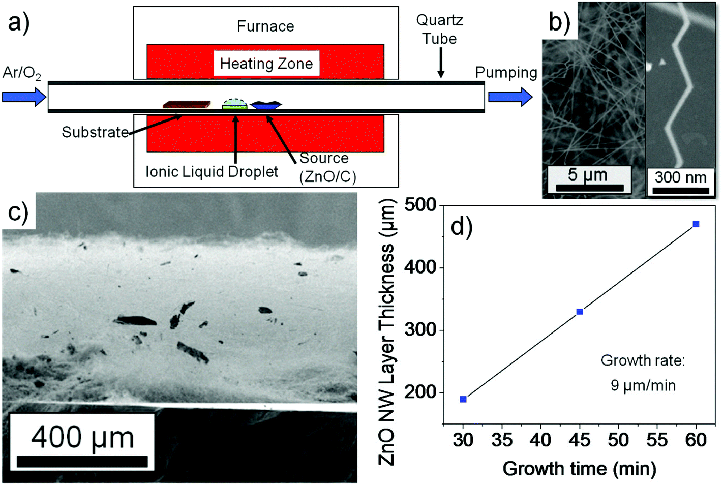 | ||
| Fig. 1 (a) Schematic diagram of the one-zone (1 in. quartz tube) thermal CVD setup to grow ZnO nanowires by an IL assisted approach. The IL droplet is placed in the upstream direction from the ZnO/C powder source. (b) SEM micrograph of the a-axis VLS ZnO nanowires. The inset shows the kinking from the a-axis nanowire growth. (c) Cross-sectioned SEM micrograph of IL ZnO nanowires. (d) Plot of ZnO nanowire layer thickness versus the growth time to determine the growth rate. | ||
Passivation of the nanowire sample surface was carried out by conformal coating with a 20 nm thick Al2O3 layer by a low temperature (115 °C) process using atomic layer deposition (ALD). Please note that the alumina was deposited onto the nanowires that were already contacted by the metal. The electrical measurements were conducted before and after the Al2O3 deposition.
In recent studies we demonstrated that the ZnO nanowire growth follows mainly a VS nanowire growth when only a ZnO + C source is used. A VLS growth is only observed in a rather specific parameter window (e.g. higher temperatures and specific Ar and O2 environments).4,6 However, controlled switching between the slow VS growth and the fast VLS growth is possible by adding the additional IL source into the growth chamber. To reverse this process to a VS growth a cleaning procedure of the CVD quartz tube reactor with HCl is needed. Fig. 1b shows randomly oriented nanowires and nanobelts grown on the Au covered Si substrate. In contrast to experiments without the IL, the nanowires are grown over almost the entire substrate area (1.5 cm × 2.5 cm), i.e. the temperature gradient effects (of up to 150 K in our case) do not seem to play a major role. Also, as seen in the cross-sectional SEM image in Fig. 1c, a highly dense ZnO nanowire film with a thickness of up to ∼450 μm is observed after only 1 hour growth. With a ZnO nanowire film growth rate of 9 μm min−1 this high-throughput nanowire growth is interesting for industrial applications, preparing papers or mats based on ZnO nanowires which could be important for medical applications. It is also very important to note that a homogeneous growth area for ZnO nanowires extends over a length of ∼7 cm (1 inch tube furnace) which represents in our system a temperature range of ∼800 °C to 950 °C (in the upstream direction). Since the nanowires based on the thin Au catalyst film grow in random interwoven orientations as indicated in Fig. 1b, we conclude from the respective observations that the nanowires have lengths of several millimeters or even centimeters as indicated in Fig. 1c. A top view of the SEM image of a ZnO nanowire sample that was grown within a time of 30 minutes can be seen in Fig. S1 in the ESI.† At the edge of this sample the nanowires show lengths of several hundred μm (e.g. >200 μm) to demonstrate that the ionic liquid assisted nanowire growth can lead to superlong nanowires. Due to the very long length, the low diameters of around 50 nm, and the ‘wool’ like structure it is rather difficult to exactly determine the length of the nanowires by SEM imaging, and therefore only estimations were made. We conducted experiments with different growth times in order to estimate the growth rate of the interwoven ZnO nanowire film. From Fig. 1d, an astonishingly tremendous ZnO nanowire film growth rate in the range of 9 μm min−1 was estimated that suggests an extremely high yield of nanowires using this IL assisted approach.
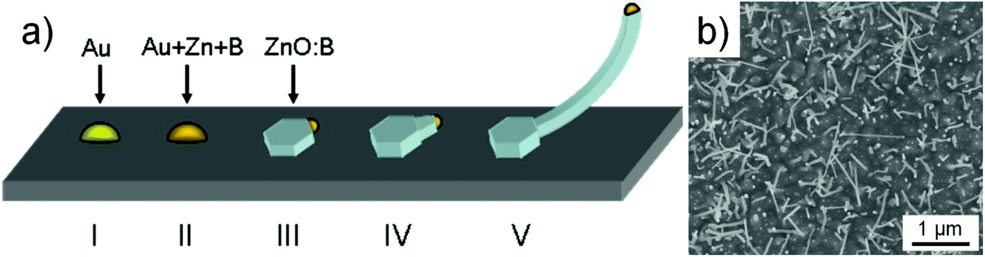
An experiment with a growth time of only 5 min was conducted on Au dots deposited on a GaN (0001)/sapphire substrate to investigate the early growth state of the nanostructure. Fig. 2b shows the nanostructure of an area with nanowires. There are Au dots typical for VLS growth observed at the tips of such nanowires. In a previous study, we had already confirmed the Au dot on the tip of the nanowires through high-resolution transmission electron microscopy (HRTEM) investigations which indicates that we have a catalyst assisted VLS nanowire growth.7 The associated electron diffraction pattern (also demonstrated previously) prove the growth of the nanowires along the a-axis. Another indication that the nanowires or nanobelts grow along the a-axis is the kinked or zigzagged growth as seen in Fig. 1b (inset). Such kinking behavior can originate from a thermal or strain instability at the liquid–solid interface because the free energy of equivalent {11![[2 with combining macron]](https://www.rsc.org/images/entities/char_0032_0304.gif) 0} planes is the same.11,12 We have also investigated the crystallographic behavior of the kinked ZnO nanowires using TEM. A bright-field TEM image that represents a kinked ZnO nanowire by this ionic liquid assisted approach is shown in Fig. S2 (ESI†). In our TEM investigations we found that the entire nanowire structure is single crystalline and no dislocations or defects can be identified at the joints and boundaries. Hence, we can conclude that the nanowire growth is single crystalline and follows a VLS mechanism along the a-axis, opposite to the normally preferred c-axis growth. At this stage, the question arises as to why the ZnO nanowires change the growth mode, the growth orientation, and so drastically the growth rate as compared to the nanowire growth without the assistance of an ionic liquid.
0} planes is the same.11,12 We have also investigated the crystallographic behavior of the kinked ZnO nanowires using TEM. A bright-field TEM image that represents a kinked ZnO nanowire by this ionic liquid assisted approach is shown in Fig. S2 (ESI†). In our TEM investigations we found that the entire nanowire structure is single crystalline and no dislocations or defects can be identified at the joints and boundaries. Hence, we can conclude that the nanowire growth is single crystalline and follows a VLS mechanism along the a-axis, opposite to the normally preferred c-axis growth. At this stage, the question arises as to why the ZnO nanowires change the growth mode, the growth orientation, and so drastically the growth rate as compared to the nanowire growth without the assistance of an ionic liquid.
 | ||
| Fig. 2 (a) Proposed growth process of the ZnO nanowires during the IL assisted VLS growth route. (b) Top view of ZnO nanowires on a GaN (1000) on the sapphire substrate using Au as a catalyst. | ||
For a deeper understanding we have to consider the composition of the used IL BMImBF4 that contains besides hydrocarbon compounds elements like N, F, and B, which may play an important role, too. Ionic liquids are in general stable salts in the liquid phase but when approaching higher temperatures above 500 °C they thermally decompose into smaller components. To our knowledge there exist no studies that investigate the decomposition of IL at temperatures such as 800 °C and higher so that we can only speculate about the behavior of such a complex system. Studies from pyrolysis-gas chromatography experiments by Ohtani et al. have shown that BMImBF4 mainly decomposes at higher temperatures (∼550 °C) by the cleavage of C–N and C–C bonds into alkyl chains but also 2-fluoropropane components were detected.8 Please note that there exist no studies so far that investigate the behavior at higher temperatures as the mentioned reference. Interestingly, no peak that originates from the boron compound appeared in their studies. We conducted XPS observations to investigate the composition of the IL assisted nanowires: no peaks that contain F or N components were observed which can be explained probably due to the detection limit of the XPS setup. However, we were able to identify a certain amount of B concentration (0.9 at%, see also Fig. 4a, upper curve) in an oxidized state. Obviously the presence of B atoms in the ZnO nanowire is comparatively higher than that of F and N. Hence, B incorporation into the ZnO nanowire affects the nanowire growth performance besides the carbon assisted growth. Additionally, we would like to suggest at this point that B substitutes Zn lattice sites. It is known that carbon can be used to assist the growth of nanowires and enhance the growth rate (not as much as we see here) but no switching in the growth orientation was observed to our knowledge.13,14 We have also conducted a reference experiment where we grew VS ZnO nanowires without using the IL to confirm that B originates from the additional IL source. The XPS result (lower curve in Fig. 4a) did not show any B related peak.
A study by Fan et al. investigated the growth of ZnO nanobelts as a response to indium dopants that appear from carbothermal evaporation of the In2O3/C system. A similar switch from c to a-orientation was observed during their study that was attributed to the incorporation of In atoms into the ZnO crystal.11,12 The generated Zn and In vapor transported to the substrate nucleates at the catalyst and forms a ternary phase (Au–Zn–In) which supersaturates in the liquid alloy droplet. Saturation and strain rise and change the surface free energy and the nanowire is layer by layer pushed out of the ZnO![[thin space (1/6-em)]](https://www.rsc.org/images/entities/char_2009.gif) :In nuclei.11,12 In this case the precipitation and oxidation of this VLS nanowire growth is now different and the a-oriented nanowires grow instead of the c-oriented. We now adapt this model to our case as described in Fig. 2a when boron is evaporated during the decomposition of BMImBF4 (please note, B and In are both group III elements). Here, similar to the VLS mechanism ZnO is formed between the liquid–solid interface but the additional boron incorporation yields the formation of a ZnO:B nucleus with a nanowire that grows out of the side facets of the Au–Zn–B alloy particle. The formation of zigzag or kinked nanowires is a further characteristic that shows similarities to the In-assisted nanowire growth as seen in Fig. 1b (inset) and in the previously reported TEM observations.7
:In nuclei.11,12 In this case the precipitation and oxidation of this VLS nanowire growth is now different and the a-oriented nanowires grow instead of the c-oriented. We now adapt this model to our case as described in Fig. 2a when boron is evaporated during the decomposition of BMImBF4 (please note, B and In are both group III elements). Here, similar to the VLS mechanism ZnO is formed between the liquid–solid interface but the additional boron incorporation yields the formation of a ZnO:B nucleus with a nanowire that grows out of the side facets of the Au–Zn–B alloy particle. The formation of zigzag or kinked nanowires is a further characteristic that shows similarities to the In-assisted nanowire growth as seen in Fig. 1b (inset) and in the previously reported TEM observations.7
Moreover, similar to the In case, the B impurities represent an n-type dopant source for the nanowires and can be utilized to enhance the electrical conductivity of the material when employed as an FET device. Hence, four-point-probe contacts were created (see Fig. 3a and b) using Al as the metal to form ohmic contacts between the metal and the ZnO n-type semiconductor.15,16 It was shown by Kim et al. that Al atoms at the Al–ZnO interface diffuse into the ZnO surface region, forming an increased doping concentration of ZnO such that n+-(Al)ZnO results (see also the schematic energy band diagram in Fig. 3c).16EV and EC represent the valence and conduction band energies, respectively, and EF represents the Fermi level. Consequently, the barrier width at the Al–ZnO interface is reduced such that a tunneling process through this barrier is enhanced. An electrical resistivity of ρ = 0.4 Ω cm was extracted from the four-point I–V curve in Fig. 4b for bare non-passivated ZnO nanowires. The ZnO nanowires have a certain amount of interface states on the surface that cause a depletion of charge carriers and also donor deactivation as schematically shown in the energy band diagram in Fig. 3d (left).17,18 If we now passivate the surface of these contacted nanowire samples with a conformal 20 nm coating of Al2O3, we reduce the amount of interface states and defects and reduce the surface depletion such that more donors are activated, as indicated in the band diagram in Fig. 3d (right).19 The now extracted electrical resistivity from passivated samples based on the I–V curve in Fig. 4b is ρ = 0.09 Ω cm, i.e. one order of magnitude less. The value is much lower than that typically obtained from VS nanowires obtained without any additional impurity source (ρ ≫ 4 Ω cm).20–22 Hence, it can be suggested that the increased value in electrical conductivity is originated by the assisted use of an ionic liquid during the nanowire growth that influences besides the morphology also the electrical properties of the ZnO nanowires.
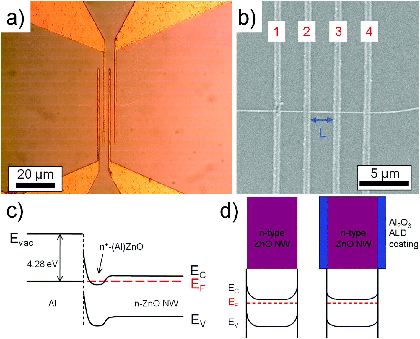 | ||
| Fig. 3 (a) Optical microscope image of a 4-probe contacted IL ZnO nanowire using Al as metal contacts. (b) SEM micrograph that shows the IL ZnO nanowire and for contact terminals to determine the resistivity. (c) Schematic band diagram of an Al-based ohmic contact on a ZnO nanowire. (d) Band diagrams of IL ZnO nanowires: (left) non-passivated nanowires, and (right) passivation with a 20 nm Al2O3 layer by ALD. EV and EC represent the valence and conduction band energies and EF represents the Fermi level. | ||
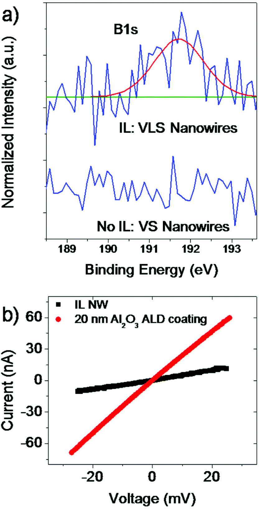 | ||
| Fig. 4 (a) XPS spectrum of IL ZnO nanowires. The lower spectrum represents reference experiments with pure VS nanowires (no IL used). (b) Electrical measurements of non-passivated (ρ = 0.4 Ω cm) and with 20 nm Al2O3 passivated (ρ = 0.09 Ω cm) IL ZnO nanowires. | ||
In conclusion, in contrast to previously reported studies, the BMImBF4 IL assisted nanowire growth utilizes mainly the components carbon and boron where boron is significantly involved in the change of the VLS nanowire growth characteristics as compared to the pure VLS ZnO nanowire growth. We discussed the two main effects that affect the ZnO nanowire growth compared to pure nanowire growth without an IL: first is that B incorporates into the ZnO lattice and induces the switching in growth orientation to a-orientation and second, the carbon that originates from the IL decomposition additionally catalyzes/enhances the nanowire growth resulting in a significantly faster growth. Both effects enable a very fast ZnO nanowire layer growth rate which was determined to be at least 9 μm min−1. Since B is an n-type source for the II/VI ZnO material, we have shown that the IL assisted growth can be used to incorporate donors. These assumptions were supported by XPS and electrical measurements of the ZnO nanowires.
Acknowledgements
This work was supported by the German Research Foundation (DFG) under the contract ZA 191/24-1 (Freiburg).References
- Y. Cui and C. M. Lieber, Science, 2001, 291, 851–853 CrossRef CAS PubMed.
- V. Schmidt, H. Riel, S. Senz, S. Karg, W. Riess and U. Gösele, Small, 2006, 2, 85–88 CrossRef CAS PubMed.
- A. Menzel, K. Subannajui, F. Güder, D. Moser and O. Paul, Adv. Funct. Mater., 2011, 21, 4342–4348 CrossRef CAS.
- A. Menzel, K. Subannajui, R. Bakhda, Y. Wang, R. Thomann and M. Zacharias, J. Phys. Chem. Lett., 2012, 3, 2815–2821 CrossRef CAS.
- A. Menzel, R. Goldberg, G. Burshtein, V. Lumelsky, K. Subannajui, M. Zacharias and Y. Lifshitz, J. Phys. Chem. C, 2012, 116, 5524–5530 CAS.
- C. Wongchoosuk, K. Subannajui, A. Menzel, I. A. Burshtein, S. Tamir, Y. Lifshitz and M. Zacharias, J. Phys. Chem. C, 2011, 115, 757–761 CAS.
- N. S. Ramgir, K. Subannajui, Y. Yang, R. Grimm, R. Michiels and M. Zacharias, J. Phys. Chem. C, 2010, 114, 10323–10329 CAS.
- H. Ohtani, S. Ishimura and M. Kumai, Anal. Sci., 2008, 24, 1335–1340 CrossRef CAS.
- K. Subannajui, C. Wongchoosuk, N. S. Ramgir, C. Wang, Y. Yang, A. Hartel, V. Cimalla and M. Zacharias, J. Appl. Phys., 2012, 112, 034311 CrossRef PubMed.
- K. L. Parry, A. G. Shard, R. D. Short, R. G. White, J. D. Whittle and A. Wright, Surf. Interface Anal., 2006, 38, 1497–1504 CrossRef CAS.
- H. J. Fan, B. Fuhrmann, R. Scholz, C. Himcinschi, A. Berger, H. Leipner, A. Dadgar, A. Krost, S. Christiansen, U. Gösele and M. Zacharias, Nanotechnology, 2006, 17, S231–S239 CrossRef CAS.
- H. J. Fan, A. S. Barnard and M. Zacharias, Appl. Phys. Lett., 2007, 90, 143116 CrossRef PubMed.
- T. Yanagida, A. Marcu, H. Matsui, K. Nagashima, K. Oka, K. Yokota, M. Taniguchi and T. Kawai, J. Phys. Chem. C, 2008, 112, 18923–18926 CAS.
- C. Cheng, T. L. Wong, W. Li, C. Zhu, S. Xu, L. Wang, K. K. Fung and N. Wang, AIP Adv., 2011, 1, 032104–032104 CrossRef PubMed.
- L. J. Brillson and Y. Lu, J. Appl. Phys., 2011, 109, 121301 CrossRef PubMed.
- K. H. Kim, K. Kim, S. Park, T. Seong and I. Adesida, J. Appl. Phys., 2003, 94, 4225 CrossRef PubMed.
- M. T. Björk, H. Schmid, J. Knoch, H. Riel and W. Riess, Nat. Nanotechnol., 2009, 4, 103–107 CrossRef PubMed.
- A. Casadei, P. Krogstrup, M. Heiss, J. A. Röhr, C. Colombo, T. Ruelle, S. Upadhyay, C. B. Sorensen, J. Nygard and A. Fontcuberta i Morral, Appl. Phys. Lett., 2013, 102, 013117 CrossRef PubMed.
- J.-P. Richters, T. Voss, D. S. Kim, R. Scholz and M. Zacharias, Nanotechnology, 2008, 19, 305202 CrossRef PubMed.
- S. N. Cha, J. E. Jang, Y. Choi, G. A. J. Amaratunga, G. W. Ho, M. E. Welland, D. G. Hasko, D.-J. Kang and J. M. Kim, Appl. Phys. Lett., 2006, 89, 263102 CrossRef PubMed.
- S. N. Cha, B. G. Song, J. E. Jang, J. E. Jung, I. T. Han, J. H. Ha, J. P. Hong, D. J. Kang and J. M. Kim, Nanotechnology, 2008, 19, 235601 CrossRef CAS PubMed.
- J. Goldberger, D. J. Sirbuly, M. Law and P. Yang, J. Phys. Chem. B, 2005, 109, 9–14 CrossRef CAS.
Footnotes |
| † Electronic supplementary information (ESI) available. See DOI: 10.1039/c4nr05426a |
| ‡ Current address: State Key Laboratory of Materials-Oriented Chemical Engineering, College of Chemistry and Chemical Engineering, Nanjing Tech University, Nanjing 210009, China. |
| This journal is © The Royal Society of Chemistry 2015 |