Far infrared-assisted embossing and bonding of poly(methyl methacrylate) microfluidic chips†
Qiwen Chen,
Luyan Zhang and
Gang Chen*
School of Pharmacy, Fudan University, 826 Zhangheng Road, Shanghai 201203, China. E-mail: gangchen@fudan.edu.cn; Fax: +86-21-51980168; Tel: +86-21-51980061
First published on 27th October 2014
Abstract
Far infrared (IR) radiation was employed in the embossing and bonding of poly(methyl methacrylate) (PMMA) microfluidic chips owing to its high penetration ability and heating efficiency. To emboss a channel plate, a piece of PMMA plate was sandwiched between a template and a glass plate. They were exposed to IR radiation for 5 min at 130 °C under pressure in a far IR-assisted embossing/bonding system. Subsequently, the embossed channel PMMA plate was bonded with a PMMA cover plate with the aid of far IR radiation and pressure. Satisfactory bonding could be achieved within 3 min at 100 °C. The fabricated microchips were successfully employed in the electrophoretic separation of four nitroaromatic compounds. Far IR-assisted embossing and bonding approaches indicate great promise for the mass production of PMMA microchips at low cost and should find a wide range of applications.
1. Introduction
Microfluidic chips have received ever-increasing research attention because of their minimal sample consumption, high performance, portability, and high degree of integration since the milestone work of Manz and Harrison.1–5 The bottleneck in the wide application of microfluidic chips is their expensive and complicated fabrication procedures.6 Hence, it is of high importance to develop low-cost fabrication strategies for the mass production of microfluidic chips.7Polymers have been widely employed in the fabrication of microfluidic devices with mass-replication technologies because they are less expensive and easier to be manipulated than glass-based materials.6–9 Poly(methyl methacrylate) (PMMA) is a commonly used thermoplastic polymer because of its ease of fabrication, low price, high optic transparency, and excellent electric and mechanical properties.10,11 The existing approaches for the fabrication of PMMA microchips include hot embossing,12 injection molding,13 room-temperature imprinting,14 solvent imprinting,15 laser ablation,16 solvent etching,17 and in situ polymerization.11 Among them, hot embossing is the most commonly used technique because it is easy to be operated.12 To emboss a channel plate, a piece of PMMA plate was covered on the surface of a silicon or metal template and was embossed under a controlled pressure at a temperature above the glass transition temperature (Tg) of PMMA (105 °C).18 The embossed channel plates bearing negative relief of channel networks need to be bonded with PMMA cover plates without the blockage and deformation of the channels.18 A series of techniques have been developed for sealing PMMA microchips, including thermal bonding,19 solvent bonding,20 in situ polymerization bonding,21 plasticizer-assisted bonding,22 microwave bonding,23 etc. Thermal bonding is the most commonly used approach because it is compatible with mass production.18,19
As two important procedures in the fabrication of PMMA microchips,8,9 hot embossing and thermal bonding were usually performed by using various hot press systems that consisted of heating devices and presses.24 The heat sources included convection oven,19 electric heating plate,25 electric heating wire,26 microwave oven,23 etc. As an important form of electromagnetic wave, infrared (IR) radiation has been widely employed as a heat source due to its high penetration ability and three-dimensional (3D) heating manner.27 Highly efficient heating can be achieved by matching the wavelength of IR radiation to the absorption characteristics of the materials.27 In previous reports, we employed IR ray as an energy source to promote proteolysis,28 solvent extraction,29 and the synthesis of graphene-based hybrids.30 As an important heating source, IR radiation indicates great promise for hot embossing and thermal bonding of PMMA microchips. However, we are not aware of early reports on the application of IR radiation in the fabrication of PMMA microfluidic chips.
In this work, far IR radiation-assisted embossing and bonding strategies were developed for the rapid and low-cost fabrication of PMMA microchips without using complicated and expensive microfabrication instruments. Under the selected conditions, satisfactory embossing and bonding could be realized within 5 and 3 min, respectively. In addition, the characterization and application of the fabricated microchips have also been described.
2. Manufacturing of far IR-assisted hot press system
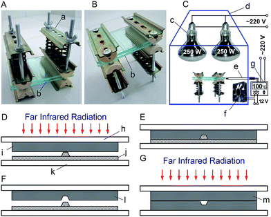
In this work, two spring-driven press devices (Fig. 1A and B) were employed to apply pressure via two pieces of transparent glass press pads (Fig. 1b, 120 × 78 × 3 mm) for the far IR-assisted embossing and bonding of PMMA microchips. The fabrication, assembly, and operation details of the press devices can be found in ESI† or our previous report.19 As shown in Fig. S1† and 1A, each press device consists of three steel clamping plates, two semicylinder silicone rubber press heads, three compression springs (spring constant, ∼1.1 kg mm−1 each), two screw bolts, and two butterfly nuts. The distance between the two screw bolts in them is 80 mm so that the glass press pads (Fig. 1b) can be inserted inside. Because the compressed springs in the press devices are assembled parallelly, the press force (F (kg)) applied on the glass press pads can be estimated based on the number of the springs (n = 6), the spring constant (k = ∼1.1 kg mm−1) as well as the length difference between the free and the compressed springs (x (mm)) by using Hooke's law (F = nkx). The maximum press force of each spring-driven press device is ∼100 kg. The pressure (P (kg cm−2)) applied on the pressed parts of the microfluidic chips and the template can be calculated based on the applied force (F (kg)) and their area (S (cm2)).As illustrated in Fig. 1C, a temperature-controllable far IR-assisted hot press system is developed for the rapid fabrication of PMMA microchips. It consists of two spring-driven press devices, two far IR lamps (wavelength, 1.72–16.6 μm; power, 250 W; Shanghai Yaming Lighting Co., Ltd, Shanghai, China),28 a thermal couple, a temperature controller, a case fan, two pieces of glass press pads, and an iron box. Both the lamps and the thermocouple are assembled in the iron case. The case fan is fixed on the sidewall of the case to drive cool air inside to adjust the temperature. The iron case has a door and several heat emission holes. The temperature controller can turn on or turn off the case fan when the temperate in the case is higher or lower than the desired temperatures (100 or 130 °C), respectively.
3. Far IR-assisted embossing
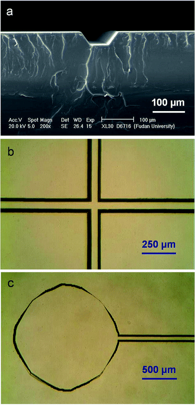
Fig. 1D–F illustrate the procedures for the far IR-assisted embossing of a PMMA channel plate. A piece of PMMA plate (Fig. 1i, 75 × 16 × 1 mm) was sandwiched between a microscopic glass slide (Fig. 3h, 76.2 × 25.4 × 1 mm) and an epoxy template (Fig. 3j) on a frosted glass plate (Fig. 3k, 76.2 × 25.4 × 1.2 mm). The epoxy templates used in this work was replicated from negative PMMA templates that were fabricated by in situ polymerization on silicon templates (see ESI†). Subsequently, they were clamped between the two glass press pads (Fig. 1b) that were assembled in the press system (Fig. 1B). The pressure applied on the PMMA plate and the template was adjusted to be ∼6 kg cm−2 by fastening the screw nuts in the two press devices to compress the springs to a desire length. After the assembled press system was placed in the far IR-assisted hot press system (Fig. 1C) upside down at 130 °C for 5 min, it was allowed to cool down to room temperature. The distance between the top of glass press pads (Fig. 1b) and the bottom surface of the lamps (Fig. 1c) was ∼12 cm. The embossed PMMA channel plate (Fig. 1l) could be easily separated from the epoxy template (Fig. 1j).Fig. 2a shows the scanning electron microscopy (SEM) image for the cross section of a replicated microchannel in an embossed PMMA channel plate. In comparison with Fig. S2,† the image of the positive relief on the epoxy template was precisely transferred into the PMMA substrate, indicating a high quality channel could be embossed with the aid of far IR radiation. The microstructure on the PMMA channel plate was examined using an optical microscope. Fig. 2b and c show the microscopic photographs of the injection cross section and the reservoir port at the end of a channel on a PMMA channel plate, respectively. The results indicated that the raised structure on the epoxy template was successfully replicated into the PMMA substrate after far IR-assisted embossing. The reproducibility of such embossing approach was studied among 50 pieces of PMMA channel plates embossed by a positive epoxy template. Satisfactory chip-to-chip reproducibility was found with the relative standard deviations (RSDs) of 3.1%, 2.8%, and 4.3% for the bottom width (51.1 μm), the top width (112.2 μm), and the depth (37.4 μm) of the embossed channels, respectively. The results implied that both the reproducibility of far IR-assisted embossing and the quality of the embossed channel plates were satisfactory.
4. Far IR-assisted bonding
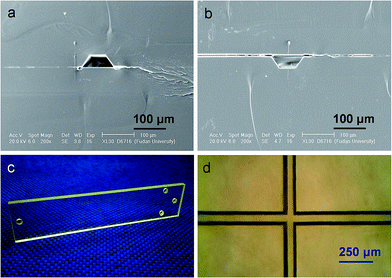
Prior to bonding, four 2 mm diameter access holes were drilled on a PMMA cover plate (Fig. 1m, 75 × 16 × 1 mm) at the sites that corresponded to the four ends of the channels on a PMMA channel plate (Fig. 1l, 75 × 16 × 1 mm; area, 12 cm2) to create reservoir ports. The channel plate and the cover plate were cleaned by sonicating in water and isopropanol for 1 min each. After being dried with a steam of compressed air, they were aligned and sandwiched between two glass slides (76.2 × 25.4 × 1 mm) that were clamped between the upper and lower glass press pads (Fig. 1b) in the spring-driven press devices. After a pressure of ∼6 kg cm−2 was applied on them by adjusting the screw nuts in the press devices, they were exposed to far IR radiation in the far IR-assisted hot press system (Fig. 1C) for 3 min at 100 °C. Other conditions were the same as those for embossing. The bonded microchip was then allowed to cool slowly to the room temperature and was removed from the glass slides. Fig. 3a illustrates the SEM image for the cross sections of a channel in a complete PMMA microchip. The PMMA cover and the PMMA channel plate merged during the far IR-assisted bonding process. No interspace between them was observed, indicating a high quality bonding. In addition, it was also found that the bonding of the PMMA microchips with the assistance of far IR radiation was fairly strong, allowing the microchips to be sawed, polished, filed, scraped, and broken without debonding. The prepared microchips could withstand an internal pressure as high as 15 MPa without breaking or leaking. Fig. S3† shows the photograph of a PMMA microfluidic chip with all channels filled by blue ink. Obviously, neither blockage nor leakage is observed.For comparison, the embossed PMMA channel plate was also bonded with a PMMA cover plate in a 100 °C convection oven for 10 min under a pressure of ∼6 kg cm−2 by using the same press system (Fig. 1A and B). As illustrated in Fig. 3b, boundaries and interspaces can be observed in the SEM image for the cross section of the microchip, implying that the bonding between the cover and the channel plates is poor in the absence of far IR radiation. During the far IR-assisted bonding, both the cover and channel plates adsorbed far IR radiation which excited the vibrations of PMMA molecules in the modes of stretching, bending, rocking, and twisting. These vibrations and the resulting molecular frictions would generate heat so that the temperature increased rapidly to realize high quality bonding.
Fig. 3c shows a typical PMMA microchip fabricated by using far IR-assisted embossing and bonding. Because PMMA chips are transparent, optical microscope was used to check the bonding quality of them. Fig. 3d illustrates the microscopic photograph of the injection cross section in a complete PMMA microchip. In comparison with the microscopic photographs of the injection cross section in an unsealed PMMA channel plate (Fig. 2b), the main channel body and cross section were complete and intact after the bonding process. Because the microchips were bonded with the aid of far IR radiation at 100 °C that was lower than the Tg of PMMA, no pronounced change and void between the covers and the channel plates was observed.
5. Application of the fabricated PMMA microchip
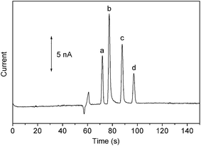
The analytical performance of the fabricated PMMA microchips was demonstrated by the electrophoretic separation of nitrobenzene (NB), 2,4-dinitrotoluene (DNT), 2,4,6-trinitrotoluene (TNT), and p-nitrobenzene (PNT) in combination with end-column amperometric detection (Fig. S4†). The procedures of electrophoretic separation and end-column amperometric deletion can be found in ESI.† Fig. 4 exhibits that the four nitroaromatic compounds are baseline resolved with plate numbers of 331![[thin space (1/6-em)]](https://www.rsc.org/images/entities/char_2009.gif) 684, 282
684, 282![[thin space (1/6-em)]](https://www.rsc.org/images/entities/char_2009.gif) 472, 316
472, 316![[thin space (1/6-em)]](https://www.rsc.org/images/entities/char_2009.gif) 850, 368
850, 368![[thin space (1/6-em)]](https://www.rsc.org/images/entities/char_2009.gif) 012 plates per meter for NB, DNT, TNT, and PNT, respectively. The half peak widths of NB, DNT, TNT, and PNT are 1.2, 1.4, 1.5, and 1.6 s, respectively, with the corresponding sensitivities of 0.68, 1.26, 0.82, and 0.41 nA ppm−1. The precision was evaluated based on nine repetitive measurements of a sample mixture containing the four nitroaromatic compounds (10 ppm). Reproducible signals were obtained with RSDs of 4.2% (NB), 2.5% (DNT), 3.8% (TNT), and 5.2% (PNT).
012 plates per meter for NB, DNT, TNT, and PNT, respectively. The half peak widths of NB, DNT, TNT, and PNT are 1.2, 1.4, 1.5, and 1.6 s, respectively, with the corresponding sensitivities of 0.68, 1.26, 0.82, and 0.41 nA ppm−1. The precision was evaluated based on nine repetitive measurements of a sample mixture containing the four nitroaromatic compounds (10 ppm). Reproducible signals were obtained with RSDs of 4.2% (NB), 2.5% (DNT), 3.8% (TNT), and 5.2% (PNT).
6. Mechanism of far IR-assisted embossing and bonding
The significantly enhanced efficiency of embossing and bonding can be attributed to far IR radiation which can excite the vibrations in PMMA molecules.28,29 These vibrations and the resulting molecular frictions would generate heat so that the temperature of the PMMA plates increased rapidly. During far IR-assisted embossing, they were heated at a temperature of 130 °C that was higher than the Tg of PMMA. The positive relief on the template was precisely transferred into PMMA substrate with the aid of pressure. In the case of far IR-assisted bonding, both channel and cover plates were pressed together. Although they were heated at a lower temperature of 100 °C, they became soft and touched each other tightly under pressure. The interaction of PMMA molecules at the interface between the channel and cover plates was enhanced in the presence of far IR radiation, resulting in a high quality bonding. Because far IR ray owned high penetration capability, it heated the PMMA plates in a 3D manner so that its heating efficiency was much higher than that of conventional hot embossing and thermal bonding in which the plates were heated in a lower efficient surface heating manner.The IR lamps used in this work can emit far IR radiation in the wavelength range of 1.72–16.6 μm (wave number, 5864 to 602 cm−1). In the FT-IR spectrum of PMMA (Fig. S5†), the absorption bands at 2996, 2951, and 1732 cm−l and in the ranges of 1365–1484 and 1149–1273 cm−1 are assigned to CH3, CH2, C![[double bond, length as m-dash]](https://www.rsc.org/images/entities/char_e001.gif) O, C–H, and C–O–C, respectively.31 Obviously, the wavenumbers of all these peaks fall into the wavenumber range of the IR ray emitted from the far IR lamps so that PMMA plates can be heated efficiently. Besides PMMA microchips, IR-assisted embossing and bonding can also be employed to fabricate other thermoplastic polymer microfluidic chips. The IR lamps should be selected based on their emission spectra and the IR adsorption spectra of polymers. The wavelength of the emitted IR radiation should match to the absorption characteristics of the polymers.
O, C–H, and C–O–C, respectively.31 Obviously, the wavenumbers of all these peaks fall into the wavenumber range of the IR ray emitted from the far IR lamps so that PMMA plates can be heated efficiently. Besides PMMA microchips, IR-assisted embossing and bonding can also be employed to fabricate other thermoplastic polymer microfluidic chips. The IR lamps should be selected based on their emission spectra and the IR adsorption spectra of polymers. The wavelength of the emitted IR radiation should match to the absorption characteristics of the polymers.
7. Conclusions
Far IR radiation was successfully employed as an efficient heating source for the rapid and low-cost fabrication of PMMA microchips by taking its advantages of high penetration ability, 3D heating manner, and high efficient heating. The ease, simplicity, versatility, and low cost of the unique embossing and bonding approaches thus make them extremely attractive for the mass production of PMMA microfluidic chips at low cost. The analytical performances of the prepared PMMA microchips have been demonstrated by electrophoretic separation of four nitroaromatic compounds. The novel far IR-assisted embossing/bonding approaches will also find wide applications in the fabrication of other thermoplastic polymer microfluidic chips.Acknowledgements
This work was financially supported by NSFC (21375023 and 21075020), State Oceanic Administration of China (201105007), and Shanghai Science Committee (12441902900).References
- D. J. Harrison, A. Manz, Z. Fan, H. Ludi and H. M. Widmer, Anal. Chem., 1992, 64, 1926 CrossRef CAS.
- D. J. Harrison, K. Flury, K. Seiler, Z. Fan, C. S. Effenhauser and A. Manz, Science, 1993, 61, 895 Search PubMed.
- A. Rios and M. Zougagh, TrAC, Trends Anal. Chem., 2013, 43, 174 CrossRef CAS.
- S. Liu, H. M. Bao, L. Y. Zhang and G. Chen, J. Proteomics, 2013, 82, 1 CrossRef CAS PubMed.
- J. Avesar, T. Ben Arye and S. Levenberg, Lab Chip, 2014, 14, 2161 RSC.
- E. Sollier, C. Murray, P. Maoddi and D. Di Carlo, Lab Chip, 2011, 11, 3752 RSC.
- C. W. Tsao and D. L. DeVoe, Microfluid. Nanofluid., 2009, 6, 1 CrossRef CAS.
- H. Becker and L. E. Locascio, Talanta, 2002, 56, 267 CrossRef CAS PubMed.
- H. Becker and C. Gartner, Anal. Bioanal. Chem., 2008, 390, 89 CrossRef CAS PubMed.
- J. C. McDonald and G. M. Whitesides, Acc. Chem. Res., 2002, 35, 491 CrossRef CAS PubMed.
- G. X. Xu, J. Wang, Y. Chen, L. Y. Zhang, D. R. Wang and G. Chen, Lab Chip, 2006, 6, 145 RSC.
- S. Z. Qi, X. Z. Liu, S. Ford, J. Barrows, G. Thomas, K. Kelly, A. McCandless, K. Lian, J. Goettert and S. A. Soper, Lab Chip, 2002, 2, 88 RSC.
- R. M. McCormick, R. J. Nelson, M. G. AlonsoAmigo, J. Benvegnu and H. H. Hooper, Anal. Chem., 1997, 69, 2626 CrossRef CAS PubMed.
- J. D. Xu, L. Locascio, M. Gaitan and C. S. Lee, Anal. Chem., 2000, 72, 1930 CrossRef CAS PubMed.
- X. H. Sun, B. A. Peeni, W. C. Yang, H. A. Becerril and A. T. Woolley, J. Chromatogr. A, 2007, 1162, 162 CrossRef CAS PubMed.
- J. Y. Cheng, C. W. Wei, K. H. Hsua and T. H. Young, Sens. Actuators, B, 2004, 99, 186 CrossRef CAS.
- P. C. Brister and K. D. Weston, Anal. Chem., 2005, 77, 7478 CrossRef CAS PubMed.
- J. Chen, Y. H. Lin and G. Chen, Electrophoresis, 2007, 28, 2897 CrossRef CAS PubMed.
- Z. Chen, L. Y. Zhang and G. Chen, Electrophoresis, 2010, 31, 2512 CrossRef CAS PubMed.
- Z. B. Gan, L. Y. Zhang and G. Chen, Electrophoresis, 2011, 32, 3319 CrossRef CAS PubMed.
- G. Chen, J. H. Li, S. Qu, D. Chen and P. Y. Yang, J. Chromatogr. A, 2005, 1094, 138 CrossRef CAS PubMed.
- H. T. Duan, L. Y. Zhang and G. Chen, J. Chromatogr. A, 2010, 1217, 160 CrossRef CAS PubMed.
- K. B. Mani, M. R. Hossan and P. Dutta, Int. J. Heat Mass Transfer, 2013, 58, 229 CrossRef CAS.
- Y. Luo, X. D. Wang and F. Yang, J. Mater. Process. Technol., 2008, 208, 63 CrossRef CAS.
- X. Wang, L. Y. Zhang and G. Chen, Anal. Bioanal. Chem., 2011, 401, 2657 CrossRef CAS PubMed.
- Z. B. Gan, Z. Y. Yu, Z. Chen and G. Chen, Anal. Bioanal. Chem., 2010, 396, 2715 CrossRef CAS PubMed.
- P. Schroeder, J. Haendeler and J. Krutman, Exp. Gerontol., 2008, 43, 629 CrossRef CAS PubMed.
- S. Wang, H. M. Bao, P. Y. Yang and G. Chen, Anal. Chem., 2008, 80, 5640 CrossRef CAS PubMed.
- H. T. Duan, Y. Chen and G. Chen, J. Chromatogr. A, 2010, 1217, 4511 CrossRef CAS PubMed.
- W. D. Qu, H. M. Bao, L. Y. Zhang and G. Chen, Chem.–Eur. J., 2012, 18, 15746 CrossRef CAS PubMed.
- K. Awazu and H. Onuki, J. Non-Cryst. Solids, 1997, 215, 176 CrossRef CAS.
Footnote |
| † Electronic supplementary information (ESI) available. See DOI: 10.1039/c4ra09909e |
| This journal is © The Royal Society of Chemistry 2014 |


