 Open Access Article
 This Open Access Article is licensed under a Creative Commons Attribution-Non Commercial 3.0 Unported Licence
Large-area arrays of three-dimensional plasmonic subwavelength-sized structures from azopolymer surface-relief gratings†
Robert J.
Moerland‡§
*,
Jenni E.
Koskela‡
,
Aleksandr
Kravchenko
,
Mikael
Simberg
,
Stefan
van der Vegte
,
Matti
Kaivola
,
Arri
Priimagi
and
Robin H. A.
Ras
*
Department of Applied Physics, Aalto University, P.O. Box 15100, FI-00076 Aalto, Helsinki, Finland. E-mail: robin.ras@aalto.fi; Tel: +358 50 432 6633
First published on 10th September 2013
Abstract
The field of plasmonics allows for confinement and control of light on the nanoscale. Due to potentially strong resonant interactions that light can have with metal nanoscale structures, metals are a good candidate to tailor interactions with light, e.g., periodic arrays of subwavelength metal structures can support extremely narrow resonances and show enhanced transmission. The field of plasmonics has evolved from using simple geometries to the desire to create complex nanostructures for improved control. The availability of fabrication techniques that provide for complex structures, however, is paired with the seemingly inevitable increase in complexity of fabrication techniques themselves. We present a facile and scalable method for the fabrication of periodic arrays of unique three-dimensional subwavelength-sized structures such as tapered holes and pyramidically shaped subwavelength-sized particles. The procedure consists of holographic inscription of a two-dimensional surface-relief grating in an azobenzene-containing polymer film, evaporative gold deposition and broad-beam ion milling of the relief structure. The method allows the fabrication of highly uniform arrays with tunable lattice parameters and dimensions over large sample areas. The optical response of the fabricated structures is determined experimentally and through simulation, which confirm the unique plasmonic response of the structures. While the proposed fabrication method has clear benefits for plasmonics, it could easily be applied also in other fields, for example by using other coating materials.
In plasmonics, nanostructured metallic surfaces are used to modify interactions between incident light and electrons in the conduction band of the metal, resulting in the creation of surface-plasmon polaritons (SPPs).1 Recent advances in nanofabrication methods enable precise control over the nanoscale features on such metal surfaces in the form of, e.g., nanoparticles, gratings, or hole arrays. By combining these fabrication techniques with theoretical modelling tools,2 tailored and complex metal structures with intriguing optical properties have been demonstrated for possible applications ranging from miniaturized optical devices to biological sensors.3 Especially, periodic arrays of subwavelength structures have gained considerable interest in the field of plasmonics. Arrays of holes in an otherwise opaque metal film became a popular topic of investigation after 1998, when Ebbesen et al. first reported the phenomenon of enhanced transmission of light through an array of holes.4 Certain wavelengths show distinctly higher transmission than what would be expected based simply on the number of holes and the transmission by a single subwavelength-sized hole. Likewise, arrays of metallic nanoparticles have been shown to be able to sustain sharply peaked resonances, due to the interaction of a lattice resonance with the local surface plasmon resonance of the individual metal nanoparticle.5,6
From an application point-of-view, molecular sensing with surface plasmon resonances (SPR)7 is based on the fact that SPR transmission spectra are sensitive to the refractive index of the dielectric medium in contact with the metal. The presence of molecules in the proximity of an SPR sensor results in a change in the effective refractive index, which can be detected as a shift in the SPR wavelength.8 Therefore, nanostructures based on plasmonics are among the most popular to build truly nanoscale sensors.9,10 Moreover, large-scale arrays of such metallic nanostructures are envisioned to find use for example in photovoltaic applications, where plasmonics could improve the efficiency of solar cells while reducing fabrication costs.11
Traditionally, nanoscale hole or particle arrays have been fabricated via electron-beam lithography (EBL)12 or focused ion beam (FIB) milling.4,13 With EBL and FIB, each structural feature is made one at a time by either sequentially exposing a layer of photoresist (EBL) for each structure, or by milling away the material from the sample (FIB) at the target location of each structure. While these methods offer high resolution and freedom in structure design, typically finite arrays of up to 50 μm in size of commonly strictly planar structures can be created, making them unsuitable for high-throughput production of large substrates. An approach to overcome the size limitation is interference lithography, which is suited for fabricating large-scale planar metallic nanohole arrays.14 The typical steps with photointerference lithography are similar to the post-processing steps necessary with EBL, such as development of the resist and lift-off procedures. By combining interference lithography and soft lithography,15,16 multiscale patterns of planar nanohole arrays have been reported.17 In such photolithography-based methods, the use of masters can be an advantage as countless copies can be replicated once the master is fabricated. However, since the fabrication of masters is subject to the already mentioned techniques, typically additional process steps are necessary to obtain non-planar structures.18 Also bottom-up fabrication techniques utilizing self-assembly of colloidal spheres are used as a self-assembled template for metal deposition.19–21 The applicability of the method is, however, often restricted by the occurrence of inherent defects in large-scale self-assembly. The increase in complexity which seems to be inevitably linked to the additional degree of freedom in the design of non-planar nanostructures highlights the need for direct three-dimensional fabrication techniques such as the recently demonstrated nanoparticle-assisted etching.22 However, none of the existing methods is able to produce complex three-dimensional nanostructures at large areas with easily variable design possibilities while keeping the fabrication scheme simple, fast and cost-effective.
An intrinsically three-dimensional fabrication route is available via the use of azobenzene-containing polymers (azopolymers). Azobenzene molecules undergo reversible trans–cis photoisomerization upon light irradiation, which actuates a cascade of motions beyond the length-scale of an individual molecule. When a thin film of an azopolymer is subjected to an interference pattern of light with spatial variation of intensity and/or polarization, the photoisomerization of azobenzene invokes mass migration of the polymer over distances of several micrometers, forming high-modulation-depth sinusoidal surface-relief gratings (SRGs) at the polymer–air interface.23,24 These SRG structures have been directly applied in various optical devices.25,26
While a comprehensive explanation for the SRG phenomenon is yet to be found and the driving mechanism depends strongly on the material system in question, there are several facts that differentiate azopolymer SRG formation from other methods of interference lithography. Firstly, the mass transport phenomenon occurs far below the glass-transition temperature of the polymer, excluding thermal effects.27 Also photoinduced crosslinking can be ruled out as the SRGs can be erased by heating.23,28 Unlike traditional photoresist materials, azopolymers do not require highly controlled humidity, temperature, and lighting conditions during fabrication. Furthermore, azopolymers typically absorb at the visible wavelength range; thus no UV light sources are required, nor is the use of master molds, mask aligners or any post-processing such as photoresist development and lift-off steps, as commonly found in standard lithographic techniques.
Herein, we describe a simple and cost-efficient approach to the fabrication of large-area arrays of three-dimensional plasmonic structures, based on SRG formation of azopolymers and ion milling. We demonstrate a variety of three-dimensional structures such as arrays of tapered holes in metal films and arrays of subwavelength-sized metallic particles with variable size and shape that otherwise can be cumbersome to manufacture. Both types of structures are of importance, since particle arrays can, e.g., modify the spectral emission properties of emitters29 and arrays of tapered holes have been shown to exhibit an enhanced extraordinary optical transmission.18 Our method of creating the SRG template combined with ion beam milling provides an easy way to vary the size, shape and periodicity of the unit cell, and structures are milled homogeneously30 over large areas up to at least several square millimeters. The largest possible size of the structures depends merely on the size of the optical inscription beam and the ion milling apparatus used, both of which are scalable. Moreover, since with our approach the azopolymer layer is an integral part of the plasmonic structure, typically fewer steps are involved in the fabrication. The fabrication method does not rely on the photoresponsive properties of any specific azobenzene–polymer system; only the intrinsic capability for SRG formation is necessary. For example, supramolecular azopolymers31–33 that are easy to prepare would also be well suited for this method. The current study complements the versatility of azobenzene-containing polymers in nanofabrication34–38 in general. We compare measured transmission spectra with simulations, which show that the fabricated structures function as expected.
The fabrication process consists of four main steps as is outlined in Fig. 1 (see also the ESI†). The fabrication begins with spin-coating a thin azopolymer film on a suitable substrate. The film is then exposed to a laser interference pattern and because of the continuous trans–cis–trans photoisomerization cycling of the azobenzene chromophores, the polymer chains move away from areas of the pattern where the grating vector and the polarization direction are parallel. Upon two orthogonal exposures, two superimposed sinusoidal gratings are formed. The patterned polymer film is then coated with gold using electron-beam deposition. In the last step, the peaks of the grating are cut away with high precision using broad-beam ion milling at a low angle of ion incidence, which results in a regular array of nano-sized structures ranging from tapered holes in the gold film to subwavelength-sized gold islands. As illustrated in Fig. 1, the gold sheet is supported by the underlying azopolymer film, i.e., the azopolymer is an integral part of the structure. Both the dimensions and periodicity of the array are tunable by varying the SRG inscription and ion milling parameters. The quality of the structure mainly depends on the quality of the SRG template, which in turn depends on the initial smoothness of the polymer film and on the optical quality of the writing beam. The unit cell of the structure is uniform throughout the milled area as the material is precisely and homogeneously removed from the surface at a pre-determined rate. In this work, we restrict the arrays to be on a square lattice, by performing two orthogonal exposures. However, the SRG formation process would also allow for the inscription of other types of structures, since the surface pattern formed is dictated merely by the spatial intensity and polarization distribution of the incident light.
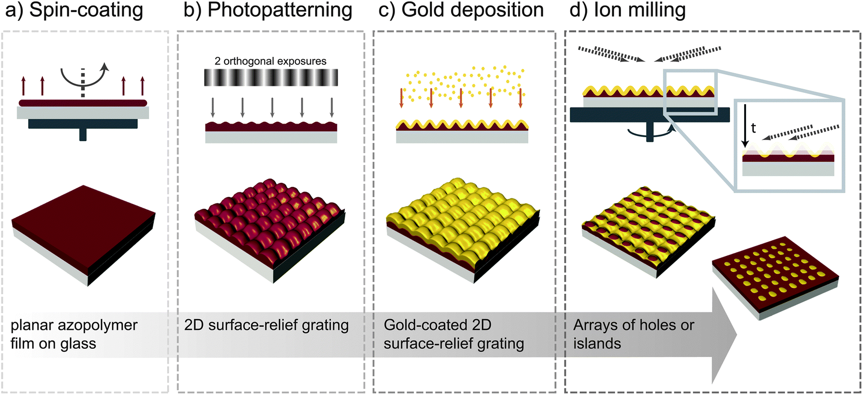 | ||
| Fig. 1 A schematic representation of the fabrication method. (a) A thin film of an azopolymer is prepared by spin-coating and (b) patterned in three dimensions using an interference pattern of laser light. (c) The patterned polymer film is coated with a layer of gold, and (d) in the last step, an array structure is generated in the gold film with ion milling. | ||
A collection of scanning-electron-microscopy (SEM) images of plasmonic array structures fabricated with the aforementioned process is shown in Fig. 2. In general, the duration of the two exposures leading to SRG formation determines the symmetry of the periodic azopolymer structure. In Fig. 2, the top row contains structures where the exposure time of the two gratings was optimized to yield a symmetric structure, whereas in the bottom row structures are shown where asymmetry was introduced on purpose. On the far left, contour maps of abstract SRGs are shown, where the double SRG is modelled as a superposition of two sinusoidal gratings39
A![[thin space (1/6-em)]](https://www.rsc.org/images/entities/char_2009.gif) cos(x) + Bcos(y); x, y = −π…π, cos(x) + Bcos(y); x, y = −π…π, | (1) |
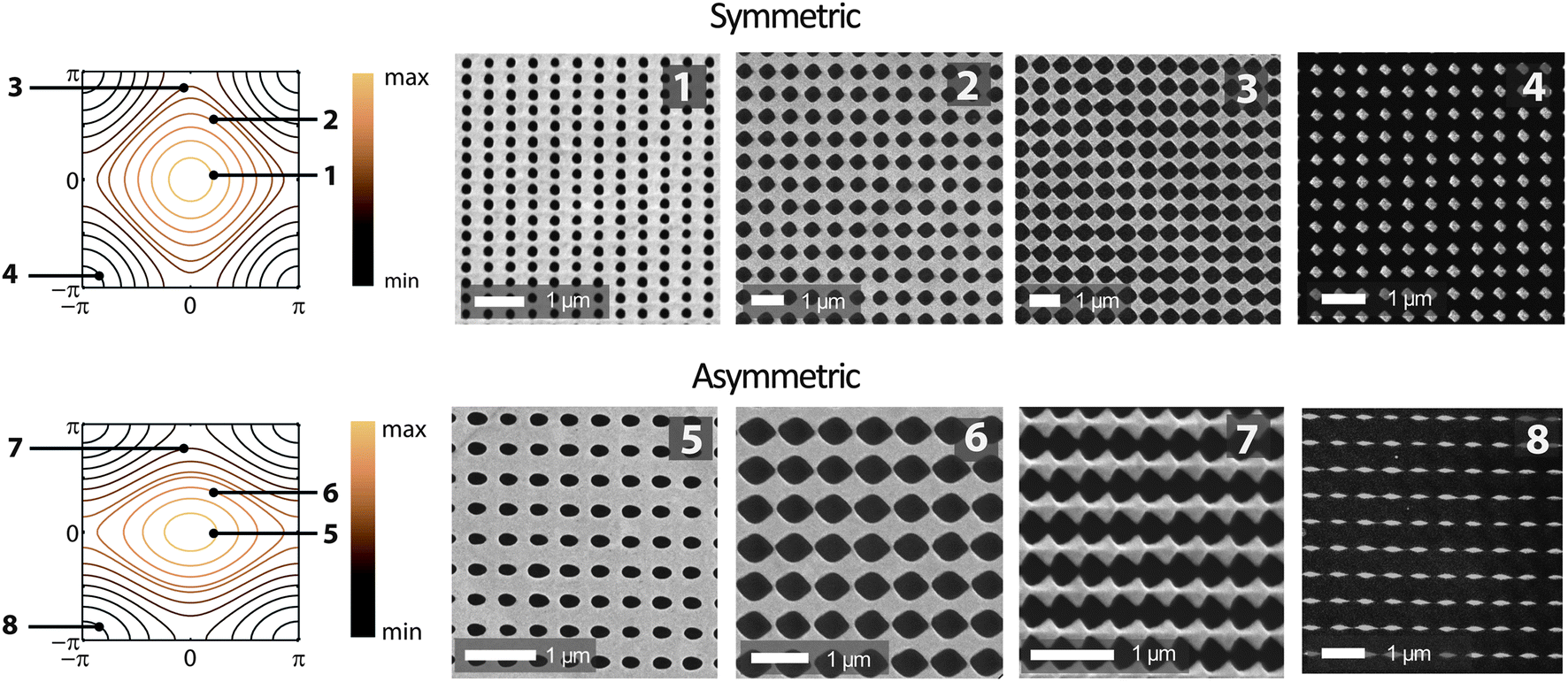 | ||
| Fig. 2 A collection of array structures fabricated with the process outlined in Fig. 1. The top row contains structures where the exposure time of the two gratings was optimized to yield a symmetric structure, whereas in the bottom row structures are shown where asymmetry was introduced on purpose. On the left, contour maps of model SRGs are shown (Acos(x) + Bcos(y); x, y = −π…π); on the top row A = B and on the bottom row A = 0.5B. Typical examples of manufactured structures that correspond to a contour in the model SRG are indicated with the numbers 1 to 8. | ||
A more detailed overview of a hole-array structure (sample 5 in Fig. 2) is shown in Fig. 3 as a collection of SEM images with different magnifications. In this particular sample, the elliptical shape of the holes is a result of the different modulation depths (A ≠ B) for the two gratings composing the 2D relief structure. The milling process thus leads to an elliptical hole shape, where the longer axis of the hole is aligned in the direction of the grating with the higher modulation depth. A fast Fourier transform analysis of the large-scale image 3a is shown in the inset as a proof of the homogeneity and periodicity over the whole area. The close-ups in 3b and c are taken at different places of the area shown in 3a, also to present the uniform quality of the hole array. As can be seen in image 3d, the holes have very smooth edges with no sign of distortion or roughness, and the size of the holes is uniform (see also the ESI†).
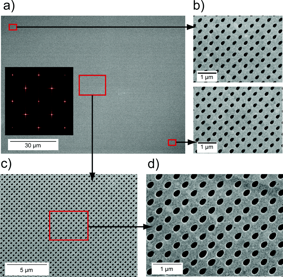 | ||
| Fig. 3 SEM images of a fabricated tapered-hole array structure (nr. 5 in Fig. 2). (a) A SEM image of a nanohole array in gold at a low magnification and a fast Fourier transform analysis of the image (inset) showing narrow peaks at the lattice frequencies and higher orders thereof, characteristic of the long-range ordering of sharply defined holes. (b) and (c) Higher-magnification SEM images taken at different locations within the image (a). (d) A higher-magnification image of (c). The images display a homogeneous array of holes with uniform size (0.036 ± 0.003 μm2, 1σ) and periodicity (460 nm) over a large area. | ||
The unique property of the hole arrays is that they are tapered, which allows for the enhancement of the extraordinary optical transmission effect.18Fig. 4a shows an SEM image of a fabricated hole array structure, taken while the sample was tilted. The modulation of both the top surface and the bottom surface of the gold layer, due to the double SRG, is visible. To clarify the difference between planar and tapered structures, we calculate the plane-wave transmission of an array of tapered holes and an array of holes in a planar gold film, each with the same periodicity (500 nm) and hole diameter (235 nm). The holes in the tapered-hole array structure are naturally filled with the azopolymer material, a dielectric. Therefore, in the case of the planar hole array, we calculate the transmission by the array with the holes filled with a vacuum (n = 1) or a dielectric (n = 1.5) to illustrate the consequence of dielectrically loading the hole.40,41 Commercially available software42 was used for this calculation. The model for the array of tapered holes is based on eqn (1), which is used to model the curvature of the polymer surface and a conformal gold layer of 150 nm on top. The gold and polymer layers are then truncated from the top (‘chopped’) to reveal a hole of diameter 235 nm. The modulation depth of the SRG was set to A = B = 125 nm. Unit cells of the modelled structures are schematically shown in Fig. 4b and the results of the calculation are displayed in Fig. 4c. For wavelengths above the diffraction edge of 750 nm, the array of tapered holes (red dashed curve) clearly shows a higher transmission than the planar arrays of holes (black solid and dotted curves), without sacrificing the extinction at the minimum, occurring at the diffraction edge. Furthermore, the transmission dip is significantly narrower for the tapered holes than for the planar counterparts, which, e.g., facilitates the detection of small changes in refractive index for sensing purposes.7
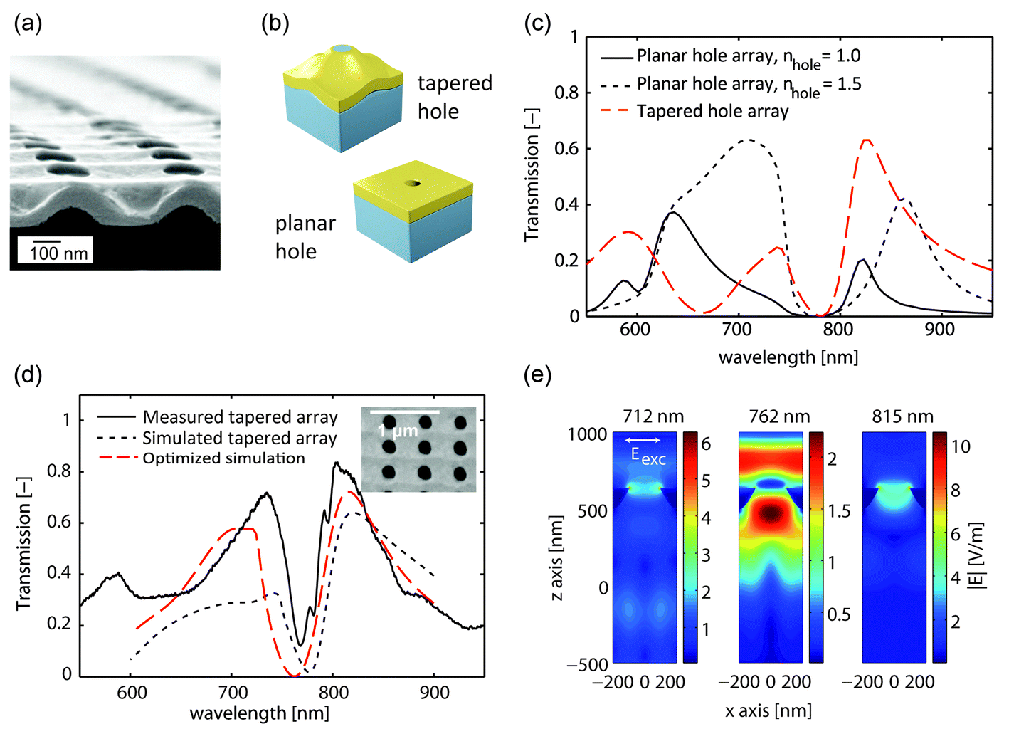 | ||
| Fig. 4 (a) SEM image of a large-area array of holes (nr. 5 in Fig. 2), taken when the sample was tilted. The modulation, due to the SRG, of both the top surface and the bottom surface of the gold layer can be clearly seen. (b) Schematic depiction of the unit cell of a tapered-hole array and a planar hole array. Eqn (1) was used to model the tapered holes. (c) The results of a calculation of the transmission by an array of tapered holes (red dashed curve) and planar arrays of holes (black solid and dotted curves). Despite the same hole diameter and gold film thickness, the array of tapered holes shows a higher peak transmittance for wavelengths longer than the diffraction edge of 750 nm, and a distinctively differently shaped spectrum. (d) The measured transmission spectrum of array number 1 in Fig. 2 is displayed (see also the inset), together with the calculated transmission spectrum (black dotted curve) of a simulation model which separately describes the modulation of the top and bottom surfaces, and is based on measured quantities. The FDTD model successfully describes the relevant spectral features. With an optimized modulation depth (A = B = 160 nm, red dashed curve), the spectrum corresponds even more closely to the measured data. (e) The absolute value of the electric field distributions for the two maxima and single minimum from (d) is shown in a cross-section through the symmetry plane of the unit cell. At the peaks, the electric field is strongly located near the rim of the tapered hole. The plane-wave excitation had a polarization as indicated in the figure and an amplitude of 1 V m−1 in all cases. | ||
Optical spectroscopy was used to study the transmission properties of the symmetric structure number 1 shown in Fig. 2 (see the ESI†). The measured transmission spectrum is denoted by the black solid curve in Fig. 4d. Note that below about 630 nm, the transmission drops due to absorption of the azobenzene molecules. We compare the acquired data with a simulation model. AFM data indicate that the top surface of the fabricated tapered-hole array has a lower peak-to-peak height difference (10 nm) than what can be expected strictly based on eqn (1) and the typical modulation depths of the SRGs (A = B = 80 nm), something that we believe can be attributed to the ion milling process, e.g., as a consequence of redeposition. Therefore, though the contours of eqn (1) accurately describe the outline of the structures formed after ion milling, a direct translation to a model as used for the calculation in Fig. 4c is too simplistic. A simple refinement is to describe the top surface of the gold and the underlying polymer SRG independently with eqn (1), with separate values for A and B for each surface. The modulation of the azopolymer surface in the model for the tapered holes was based on AFM height data typical for the SRGs formed after two exposures (80 nm) and the modulation of the topmost gold surface was based on AFM height data after ion milling (10 nm). The height of the polymer SRG is truncated such that a flat, near-circular opening with a diameter of 235 nm is obtained as confirmed by SEM and AFM data. Overall, the match between the measured and calculated spectra shown in Fig. 4d is quite good: all features in the measured transmission spectrum are reproduced in the calculation, at the right location and with roughly the correct amplitude. The most striking difference is that the measured spectrum has a minimum that is even narrower than the calculated spectrum. An optimized set of parameters yields a better correspondence between the measured transmission spectrum and the calculation, but indicates a stronger modulation of the bottom surface (160 nm). For the optimized model, the absolute values of the electric-field distributions is shown for the two maxima and the single minimum in a cross-section through the symmetry plane of the unit cell. At the maximum transmittance, the electric field is strongly confined to the area near the rim of the tapered hole.
Finally, we show the transmission spectrum of gold subwavelength-sized islands (sample number 4 in Fig. 2) in Fig. 5 (solid black curve). In the case of an array of nanoparticles, sharp dips in the transmission spectra can occur when the nanoparticles are embedded in a (near) homogeneous environment.5,6 Here, this is achieved by adding immersion oil onto the sample and placing a glass cover slip on top. Therefore, the refractive index of the surroundings of the subwavelength-sized islands is n ≈ 1.5. The clear, narrow dip in the transmission spectrum, corresponding to a surface lattice resonance, shows that also this type of array can be successfully fabricated with the azopolymer SRG/ion milling method. For comparison purposes, the system is approximated by two models. The first is an infinite array of pyramids with a square base of 230 nm and a height of 60 nm, rotated around the normal of the base such that the lattice vectors of the array and the sides of the base are at a 45-degree angle. The second model is an infinite array of squares with sides of 230 nm and a thickness of 90 nm, rotated in the same way as the pyramids. The lengths of the base of the pyramid and the sides of the squares are based on SEM data, as is the period of the arrays (500 nm). The height of the pyramid is based on AFM data. The thickness of the squares is obtained from an optimization sequence to match the transmission spectrum as closely as possible. The results of this calculation are shown in Fig. 5 as well. Despite the fact that the exact geometry of the island is not fully known, especially underneath the gold surface, all main spectral features are reproduced satisfactorily by the pyramidal model which contains no free parameters. The model with squares provides an even closer match, but indicates that further research is necessary to model the fabricated structures to full accuracy.
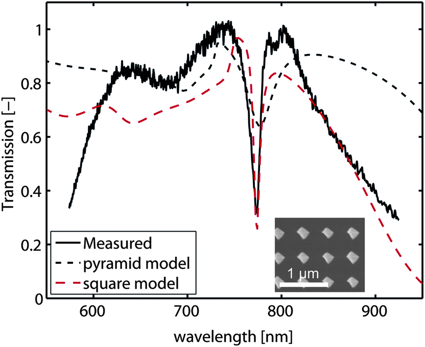 | ||
| Fig. 5 Transmission spectrum of a sample containing an array of subwavelength-sized gold islands in a near-homogeneous (n ≈ 1.5) environment. The clear dip in the transmission spectrum corresponds to a surface lattice resonance and shows that also this type of array can be successfully fabricated with the azopolymer SRG/ion milling method. A simple simulation model with a pyramidically shaped subwavelength-sized particle, based on AFM data, satisfactorily reproduces all the main spectral features (black dotted curve). A model based on a square, rotated by 45 degrees with respect to the grating vectors and along the normal of the substrate, provides a closer match if the thickness is optimized to match the measured data (red dashed curve). | ||
Summarizing, we have developed a new approach to produce arrays with long-range periodic order of three-dimensional subwavelength-sized structures ranging from tapered holes to checkerboards and islands. Starting from a two-dimensional grating pattern on a thin azopolymer film, various arrays with plasmonic properties were fabricated by electron-beam metal deposition and ion milling. The fabricated arrays of subwavelength-sized structures exhibit non-trivial optical transmission properties which are reproduced to reasonable precision with simplified simulation models. The method is, however, not limited to grating-based patterns, as the surface pattern formed is dictated merely by the spatial intensity and polarization distribution of the incident light. In contrast to other work on interference lithography that utilizes the polymer layer merely as a sacrificial template, our method shows more versatility as it could enable further use of the underlying azopolymer layer for the optical modification of the transmission properties of the structures, by employing the photo-orientability of azobenzene molecules. Furthermore, the proposed method is fast and cost-effective in comparison with EBL, FIB or nanophotolithography as the azopolymer-based surface patterning does not require molding, UV light sources or mask aligners, nor does it need any post-processing steps such as photoresist development. Essentially, the method can be scaled up to much larger arrays than what is presented in this paper, as the underlying physical phenomena pose no fundamental limitations when it comes to sample size, and larger area optical setups and ion milling devices are commercially available. This is a major asset to the method as larger metal surfaces are easier to implement into sensor devices and other applications without compromising the sensitivity of the plasmonic response. While this work has been aimed at providing a new way to produce nanopatterned gold surfaces for plasmonics, possible applications of the proposed technique are manifold and we foresee a wider use of it also outside the plasmonics or nanophotonics realm.
The authors acknowledge financial support from the Academy of Finland (PHORMAT project 135159 and 135106). AP acknowledges the support provided by the Japan Society for the Promotion of Science and the Foundations' Post Doc Pool in Finland. Hua Jiang is acknowledged for discussions on ion milling, Antti Soininen is acknowledged for help with AFM imaging, Juuso Korhonen is acknowledged for help with SEM imaging, and Andriy Shevchenko is acknowledged for fruitful conversations related to this article. This work made use of the Aalto University Nanomicroscopy Center (Aalto-NMC) premises.
References
- W. L. Barnes, A. Dereux and T. W. Ebbesen, Nature, 2003, 424, 824–830 CrossRef CAS PubMed.
- J. M. Montgomery, T.-W. Lee and S. K. Gray, J. Phys.: Condens. Matter, 2008, 20, 323201 CrossRef.
- S. A. Maier and H. A. Atwater, J. Appl. Phys., 2005, 98, 011101 CrossRef.
- T. W. Ebbesen, H. J. Lezec, H. F. Ghaemi, T. Thio and P. A. Wolff, Nature, 1998, 391, 667–669 CrossRef CAS PubMed.
- S. Zou, N. Janel and G. C. Schatz, J. Chem. Phys., 2004, 120, 10871–10875 CrossRef CAS PubMed.
- B. Auguié and W. L. Barnes, Phys. Rev. Lett., 2008, 101, 143902 CrossRef.
- J. Homola, S. S. Yee and G. Gauglitz, Sens. Actuators, B, 1999, 54, 3–15 CrossRef CAS.
- A. De Leebeeck, L. K. S. Kumar, V. de Lange, D. Sinton, R. Gordon and A. G. Brolo, Anal. Chem., 2007, 79, 4094–4100 CrossRef CAS PubMed.
- R. Gordon, D. Sinton, K. L. Kavanagh and A. G. Brolo, Acc. Chem. Res., 2008, 41, 1049–1057 CrossRef CAS PubMed.
- M. E. Stewart, C. R. Anderton, L. B. Thompson, J. Maria, S. K. Gray, J. A. Rogers and R. G. Nuzzo, Chem. Rev., 2008, 108, 494–521 CrossRef CAS PubMed.
- H. A. Atwater and A. Polman, Nat. Mater., 2010, 9, 205–213 CrossRef CAS PubMed.
- M. Najiminaini, F. Vasefi, B. Kaminska and J. J. L. Carson, Opt. Express, 2010, 18, 22255–22270 CrossRef PubMed.
- K. L. van der Molen, K. J. Klein Koerkamp, S. Enoch, F. B. Segerink, N. F. van Hulst and L. Kuipers, Phys. Rev. B: Condens. Matter Mater. Phys., 2005, 72, 045421 CrossRef.
- J. W. Menezes, J. Ferreira, M. J. L. Santos, L. Cescato and A. G. Brolo, Adv. Funct. Mater., 2010, 20, 3918–3924 CrossRef CAS.
- E.-S. Kwak, J. Henzie, S.-H. Chang, S. K. Gray, G. C. Schatz and T. W. Odom, Nano Lett., 2005, 5, 1963–1967 CrossRef CAS PubMed.
- D. Qin, Y. Xia and G. M. Whitesides, Nat. Protoc., 2010, 5, 491–502 CrossRef CAS PubMed.
- J. Henzie, M. H. Lee and T. W. Odom, Nat. Nanotechnol., 2007, 2, 549–554 CrossRef CAS PubMed.
- J.-C. Yang, H. Gao, J. Y. Suh, W. Zhou, M. H. Lee and T. W. Odom, Nano Lett., 2010, 10, 3173–3178 CrossRef CAS PubMed.
- W. A. Murray, S. Astilean and W. L. Barnes, Phys. Rev. B: Condens. Matter Mater. Phys., 2004, 69, 165407 CrossRef.
- E. M. Hicks, X. Zhang, S. Zou, O. Lyandres, K. G. Spears, G. C. Schatz and R. P. Van Duyne, J. Phys. Chem. B, 2005, 109, 22351–22358 CrossRef CAS PubMed.
- V. Canpean and S. Astilean, Mater. Lett., 2009, 63, 2520–2522 CrossRef CAS PubMed.
- T. James, Y. V. Kalinin, C.-C. Chan, J. S. Randhawa, M. Gaevski and D. H. Gracias, Nano Lett., 2012, 12, 3437–3442 CrossRef CAS PubMed.
- N. K. Viswanathan, D. Y. Kim, S. Bian, J. Williams, W. Liu, L. Li, L. Samuelson, J. Kumar and S. K. Tripathy, J. Mater. Chem., 1999, 9, 1941–1955 RSC.
- A. Natansohn and P. Rochon, Chem. Rev., 2002, 102, 4139–4176 CrossRef CAS PubMed.
- T. Alasaarela, D. Zheng, L. Huang, A. Priimagi, B. Bai, A. Tervonen, S. Honkanen, M. Kuittinen and J. Turunen, Opt. Lett., 2011, 36, 2411–2413 CrossRef PubMed.
- L. M. Goldenberg, V. Lisinetskii, Y. Gritsai, J. Stumpe and S. Schrader, Opt. Mater. Express, 2012, 2, 11–19 CrossRef CAS.
- K. G. Yager and C. J. Barrett, J. Chem. Phys., 2004, 120, 1089–1096 CrossRef CAS PubMed.
- J. Vapaavuori, A. Priimagi and M. Kaivola, J. Mater. Chem., 2010, 20, 5260–5264 RSC.
- G. Vecchi, V. Giannini and J. Gómez Rivas, Phys. Rev. Lett., 2009, 102, 146807 CrossRef CAS.
- X. D. Wang, E. Graugnard, J. S. King, Z. L. Wang and C. J. Summers, Nano Lett., 2004, 4, 2223–2226 CrossRef CAS.
- O. Kulikovska, L. M. Goldenberg and J. Stumpe, Chem. Mater., 2007, 19, 3343–3348 CrossRef CAS.
- J. Gao, Y. He, F. Liu, X. Zhang, Z. Wang and X. Wang, Chem. Mater., 2007, 19, 3877–3881 CrossRef CAS.
- J. E. Koskela, J. Vapaavuori, J. Hautala, A. Priimagi, C. F. J. Faul, M. Kaivola and R. H. A. Ras, J. Phys. Chem. C, 2012, 116, 2363–2370 CAS.
- S.-S. Kim, C. Chun, J.-C. Hong and D.-Y. Kim, J. Mater. Chem., 2006, 16, 370–375 RSC.
- L. Li, F. Yan, M. Cazeca, L. Samuelson and J. Kumar, J. Macromol. Sci., Part A: Pure Appl. Chem., 2007, 44, 1299–1303 CrossRef CAS.
- S. Lee, J. Shin, Y.-H. Lee, S. Fan and J.-K. Park, Nano Lett., 2010, 10, 296–304 CrossRef CAS PubMed.
- S. Lee, J. Shin, Y.-H. Lee and J.-K. Park, ACS Nano, 2010, 4, 7175–7184 CrossRef CAS PubMed.
- A. Kravchenko, A. Shevchenko, V. Ovchinnikov, A. Priimagi and M. Kaivola, Adv. Mater., 2011, 23, 4174–4177 CrossRef CAS PubMed.
- L. Lévesque and P. Rochon, J. Opt. Soc. Am. A, 2005, 22, 2564–2568 CrossRef.
- F. García de Abajo, Opt. Express, 2002, 10, 1475–1484 CrossRef.
- F. J. García-Vidal, L. Martín-Moreno, T. W. Ebbesen and L. Kuipers, Rev. Mod. Phys., 2010, 82, 729–787 CrossRef.
- Lumerical Solutions, Inc., http://www.lumerical.com.
Footnotes |
| † Electronic supplementary information (ESI) available: Details on sample fabrication, the measurement setup used for optical transmission experiments and a statistical image analysis of sample homogeneity. See DOI: 10.1039/c3mh00008g |
| ‡ These authors contributed equally to this work. |
| § Present address: TU Delft, P.O. Box 5046, NL-2600 GA Delft, The Netherlands, E-mail: E-mail: r.j.moerland@tudelft.nl |
| This journal is © The Royal Society of Chemistry 2014 |