
 Open Access Article
 This Open Access Article is licensed under a Creative Commons Attribution-Non Commercial 3.0 Unported Licence
Patterning of amorphous-InGaZnO thin-film transistors by stamping of surface-modified polydimethylsiloxane†
Chungwan
Gu
and
Jang-Sik
Lee
*
Department of Materials Science and Engineering, Pohang University of Science and Technology (POSTECH), Pohang 790-784, Republic of Korea. E-mail: jangsik@postech.ac.kr
First published on 21st April 2016
Abstract
An indium gallium zinc oxide (IGZO) layer was patterned and thin-film transistors (TFTs) were fabricated by surface modified polydimethylsiloxane (PDMS) stamping and IGZO solution. The PDMS stamp was prepared by immersion in piranha solution and treatment with UV–ozone to make a hydrophilic surface. Patterned PDMS was inked by contact with the IGZO layer, and then stamped on the desired substrate. The process did not cause etching damage, so the stamped amorphous-IGZO TFTs showed low leakage current of ∼10−11 A, high on/off current ratio of ∼108, carrier mobility of 6 cm2 V−1 s−1, and narrow hysteresis of 0.2 V. UV irradiation on the IGZO layer caused a photochemical annealing effect that improved the electrical properties of IGZO TFTs. This method provides a simple and versatile process to fabricate transparent metal-oxide TFTs based on patterning the devices by reusable stamping methods.
Introduction
Metal-oxide-based thin-film transistors (TFTs), especially amorphous indium gallium zinc oxide (a-IGZO)-based TFTs, have good characteristics including high electron mobility and transparency, and are therefore regarded as essential elements for displays, organic light-emitting diodes (OLEDs) and optoelectronic devices.1–5 Recent advances in this field have achieved carrier mobility of higher than 10 cm2 V−1 s−1.6–8 Metal-oxide-based TFTs can be fabricated using vacuum processes, such as pulsed laser deposition1 and radio frequency (RF) sputtering.9,10 However, vacuum deposition has disadvantages, such as slow fabrication and high cost. As an alternative, solution processes including inkjet printing,11 spin-coating,12 and dip-coating,13 can be used to fabricate devices under ambient conditions.The patterning process is very important in fabrication and integration of semiconductor devices. Precise fabrication can reduce the leakage current between adjacent devices. Among various patterning technologies, photolithography has been most widely used, but it has disadvantages, such as high production cost and complicated process. In addition, chemicals used to etch thin films can affect the electrical properties, such as carrier mobility, leakage current, threshold voltage, and hysteresis. Printing methods, such as ink-jet printing and electro-hydrodynamic-jet printing, are emerging alternatives to photolithography,11 but these methods also have limitations, such as slow fabrication and nozzle clogging.
Recently, patterning techniques on polydimethylsiloxane (PDMS) elastomer such as nano-imprinting and direct transfer of materials have been introduced. Direct transfer of a-IGZO onto PDMS is reported using RF magnetron sputtering.14 ZnO has been patterned by chemical imprinting with a PDMS stamp that had been soaked in ammonia solution and used to selectively dissolve ZnO.15 Zinc tin oxide (ZTO) stripe patterns have been fabricated by exploiting capillary force to draw ZTO solution into stripe patterns of PDMS.16 However, to fabricate devices these methods still require several steps.
In this research, we suggest PDMS stamping to transfer the IGZO layer for a low-cost and high-speed fabrication method. To give appropriate properties to the PDMS surface, PDMS elastomer was immersed in piranha solution to remove hydrophobic methyl groups. Then the PDMS surface was UV–ozone treated to make it hydrophilic. IGZO solution was transferred by PDMS stamping and subjected to a combination of photochemical and thermal annealing. The IGZO was not damaged by chemical etchant, so patterning decreased leakage current and narrowed the hysteresis loop. The patterned PDMS stamps can be reused many times. We show the possibility of using IGZO solution and PDMS to pattern the active layer of the TFTs.
Experimental
IGZO solution preparation
All chemicals were purchased from Sigma-Aldrich and used without further purification. Metal precursors, that is, indium nitrate hydrate (In(NO3)3·xH2O, 99.9%), gallium nitrate hydrate (Ga(NO3)3·xH2O, 99.9%) and zinc acetate dihydrate (Zn(CH3CO2)2·2H2O, 98%), were 0.125 M and were mixed at a mole ratio of In![[thin space (1/6-em)]](https://www.rsc.org/images/entities/char_2009.gif) :Ga:Zn = 7:1:2. Metal precursors were dissolved in 2-methoxyethanol (2-ME, CH3OCH2CH2OH, anhydrous 99.8%) and stirred thoroughly for 6 h at 75 °C to make the transparent and homogeneous solution.17 Ethylene glycol (EG) was added to synthesize the EG/IGZO solution. The volume ratio was 2-ME:EG = 20:1. Solution viscosity was controlled by adjusting the amount of EG. IGZO solutions were filtered using 0.2 μm syringe filters (PTFE, Whatman) before being spin-coated.
:Ga:Zn = 7:1:2. Metal precursors were dissolved in 2-methoxyethanol (2-ME, CH3OCH2CH2OH, anhydrous 99.8%) and stirred thoroughly for 6 h at 75 °C to make the transparent and homogeneous solution.17 Ethylene glycol (EG) was added to synthesize the EG/IGZO solution. The volume ratio was 2-ME:EG = 20:1. Solution viscosity was controlled by adjusting the amount of EG. IGZO solutions were filtered using 0.2 μm syringe filters (PTFE, Whatman) before being spin-coated.
Fabrication of patterned PDMS stamps and surface modification
PDMS elastomer (Sylgard 184) was purchased from Dow Corning. Sylgard 184 base and curing agent in 10:1 (w:w) ratio were mixed thoroughly and poured onto the master substrate in a Petri dish. Air bubbles generated during mixing were removed completely in a vacuum chamber. The PDMS was cured at 75 °C for 6 h, and then peeled off smoothly from the master substrate.18–20 PDMS for IGZO transfer was thermally annealed at 100 °C for 1 d in an oven, and then immersed in piranha solution (H2SO4:H2O2 = 1:1 mol:mol). The PDMS was removed from the solution, followed by a thorough rinse with deionized (DI) water to remove chemical residue. For ozone treatment, the sample was illuminated using a low-pressure mercury lamp (wavelength λ = 254 nm (90%) and 185 nm (10%)) for 30 min.
Fabrication of stamped a-IGZO TFTs
Highly doped n-type Si wafer with 100 nm SiO2 was used as the substrate. Before device fabrication the wafers were cleaned in a piranha solution (H2SO4:H2O2 = 4:1 mol:mol), sonicated sequentially in acetone, ethanol, and DI water for 15 min each, and then dried under N2 gas. Finally, the wafers were treated with UV–ozone for 10 min to remove organics and clean the surface.
IGZO solution was spin-coated on the wafer at 500 rpm for 5 s, and then at 3000 rpm for 30 s. The PDMS stamp was attached to a substrate coated with IGZO solution (Fig. 1a). Hydrophilic modified PDMS was put on the IGZO spin-coated layer for several seconds under pressure, and then peeled off and immediately stamped onto the new substrate (Fig. 1b). After peeling off, patterned IGZO on the substrate was annealed photochemically for 1 h, and then annealed thermally at 350 °C for 1 h (Fig. 1c). After annealing, Al (100 nm) was deposited through a shadow mask by electron-beam evaporation (Fig. 1d). To compare the effect of PDMS stamping, IGZO TFTs without patterns were also fabricated by spin coating.
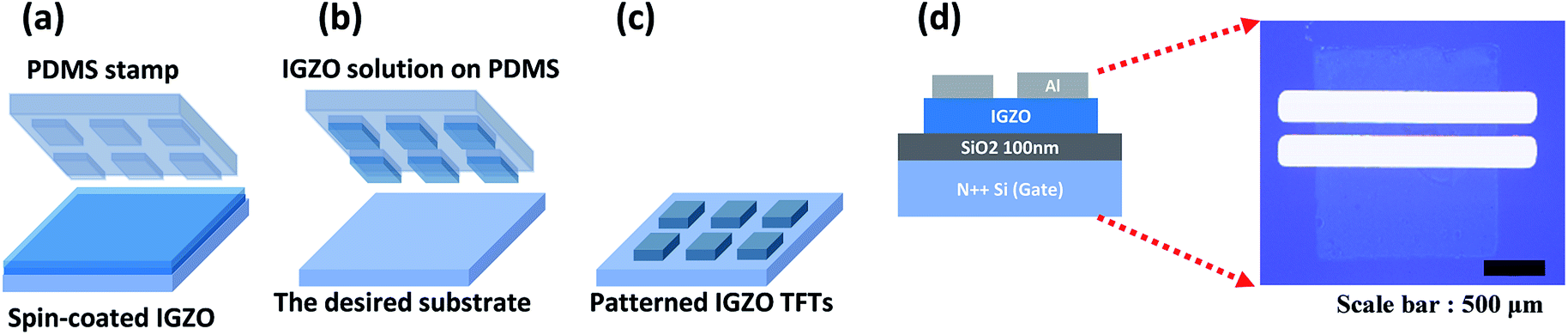 | ||
| Fig. 1 Schematic of fabrication procedures. (a) PDMS stamp and spin-coated IGZO layer. (b) PDMS stamp with IGZO ink and desired substrate. (c) IGZO transfer to the desired substrate. (d) Cross-sectional view of final device structure. (Right image: optical microscope image of the fabricated device.) | ||
Characterization
The contact angle of IGZO solution on PDMS was measured using the contact angle measurement system (SmartDrop). Images of solution droplets were taken by a high-resolution CCD camera. The electrical properties of TFTs were analyzed in the dark using semiconductor parameter analyzer (KEITHLEY 4200-SCS). Surface roughness and IGZO layer thickness were measured using atomic force microscopy (AFM, VEECO Dimension 3100) and Alpha-Step (KLA-Tencor), respectively.Results and discussion
Surface treatment of PDMS
The PDMS stamp surface is intrinsically hydrophobic with low surface energy because it is coated with nonpolar methyl groups. 2-ME-based IGZO solution is polar so it does not wet well onto PDMS. Dipping PDMS in piranha solution and UV–ozone treatment made the PDMS surface hydrophilic. Before wet chemical treatment, PDMS was thermally aged at 100 °C for 1 d in an oven. Low molecular weight (LMW) species such as uncrosslinked PDMS chains or residual crosslinking chains may be volatilized during thermal aging.21 The decrease in the amount of LMW species helps to stabilize the hydrophilic surface after wet chemical treatment. After thermal aging, PDMS surface was first modified by dipping it in piranha solution. Oxygen generated in piranha solution reacted with PDMS to form polar hydrophilic silanol groups. Contact angles decreased with as UV–ozone treatment time increased after dipping the PDMS stamp in piranha solution (Fig. 2). The 185 nm irradiation induces formation of ozone from oxygen in the air. The organic contamination can also be removed by reaction with ozone driven by irradiation at λ = 254 nm. The PDMS surface becomes oxidized and hydrophilized.22,23 2-ME-based IGZO solution was wetted on the PDMS surface. Excessive UV–ozone treatment (>30 min) caused the PDMS to crack. | ||
| Fig. 2 Contact angles vs. UV–ozone treatment time. Insets: optical images of IGZO solution droplet on PDMS. | ||
The volume of solution transferred from PDMS to substrate has an effect on the thickness of active layers. Although the volume of solution transferred cannot be measured precisely, it can be controlled by adjusting stamping pressure. When the PDMS stamp was not surface treated, the transfer failed (Fig. S1†).
Characteristics of stamped IGZO TFTs
Output and transfer characteristics (Fig. 3) were obtained from the measurement of spin-coated and single-stamped IGZO TFTs. To obtain output curves, drain voltage (Vd) was swept from 0 V to 30 V at fixed gate voltage (Vg) in increments of 5 V. To obtain transfer curves, Vg was swept from −20 V to 30 V to −20 V at Vd = 30 V. Spin-coated IGZO showed threshold voltage (Vth) of ∼3 V and narrow hysteresis, but high leakage current (ILEAK) (Fig. 3a). In contrast, stamped IGZO showed ILEAK as low as 10−11 A with still narrow hysteresis and low Vth (Fig. 3b). | ||
| Fig. 3 Electrical properties of IGZO TFTs. (a) Output and (b) transfer characteristics of spin-coated IGZO TFTs. (c) Output and (d) transfer characteristics of stamped IGZO TFTs (single-stamped IGZO). | ||
The root mean-square roughness (RRMS) of spin-coated and single-stamped IGZO surface was measured using AFM (Fig. 4). The average RRMS was 0.196 nm and 0.352 nm on the spin-coated IGZO surface and stamped IGZO surface, respectively. The thickness of IGZO layer was measured using a stylus profiler. The thickness was ∼15 nm in both the single-stamped and spin-coated layers. The small RRMS and uniform thickness demonstrate that uniform layers can be synthesized by PDMS stamping. The stamping method transfers IGZO solution directly to the desired substrate and does not require chemicals to etch thin films, whereas conventional device fabrication does. As a result, uniform layers with good electrical properties can be achieved by this stamping method.
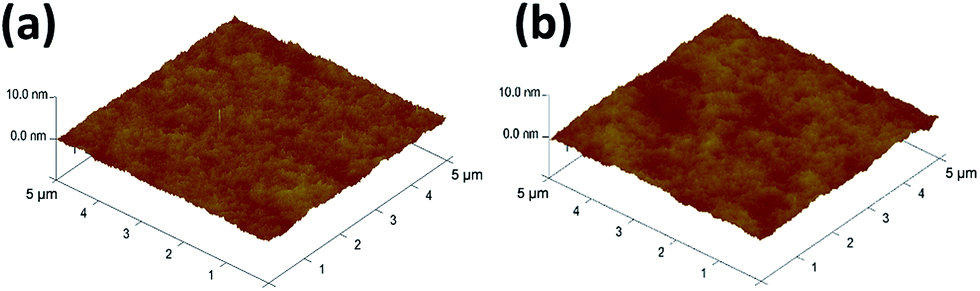 | ||
| Fig. 4 Atomic force microscopy images of IGZO TFTs. (a) Spin-coated IGZO. (b) Single-stamped IGZO. | ||
To improve electrical properties, photochemical annealing was done.17 UV absorbance of IGZO solution increased near λ = 254 nm (Fig. S2†). When UV irradiates IGZO solution, alkoxy groups can be broken by photochemical energies, and metal and oxygen atoms are activated to form metal–oxygen–metal (M–O–M) networks. Compared to thermal annealing alone, photochemical annealing improves the electrical properties (Fig. 5).22,24,25
 | ||
| Fig. 5 Electrical properties with and without photochemical annealing of single-stamped IGZO TFTs. (a) Output curves. (b) Transfer curves. Red line, thermal annealing after photochemical annealing. Black line, thermal annealing only. | ||
Carrier mobility μ is calculated using the following equation:26
| Id = (W/(2L))μCox(Vg − Vth)2, Vd > (Vg − Vth), (saturation) |
As the number n of stampings increased, μ increased and Vth shifted negatively from 6.2 V to −6.7 V (Fig. 6). As n rose, the thickness of IGZO layers increased. When IGZO solution is stamped on the IGZO layer, the pores or pin-holes may be filled by subsequent stampings (Fig. S3†). Accumulation of free carriers and the decreasing number of defects lead to increased μ and a negative shift in Vth.28 These results demonstrate that the electrical properties of the TFT can be controlled by adjusting the number of stacked layers (Fig. S4†).
 | ||
| Fig. 6 Electrical characteristics of IGZO TFTs as a function of stamping numbers. | ||
Conclusions
We developed a-IGZO TFTs by using surface-modified, patterned PDMS to stamp an IGZO layer. The patterned IGZO obtained by PDMS stamping had high μ, low Vth and high on/off ratio. In particular, lower leakage current and hysteresis were obtained with the PDMS stamping method than by conventional spin-coating. PDMS stamping is a simple, inexpensive, and fast fabrication method. In addition, the stamp can be reused. The proposed method may reduce the time and cost of fabricating a-IGZO TFTs, and may also have other applications.Acknowledgements
This work was supported by the National Research Foundation of Korea (NRF-2015R1A2A1A15055918), and Future Semiconductor Device Technology Development Program (10045226) funded by the Ministry of Trade, Industry & Energy (MOTIE)/Korea Semiconductor Research Consortium (KSRC). In addition, the work was partially supported by the Brain Korea 21 PLUS project (Center for Creative Industrial Materials).Notes and references
- K. Nomura, T. Kamiya, H. Ohta, K. Ueda, M. Hirano and H. Hosono, Appl. Phys. Lett., 2004, 85, 1993 CrossRef CAS.
- H. Hosono, Thin Solid Films, 2007, 515, 6000–6014 CrossRef CAS.
- B. D. Ahn, H.-J. Jeon, J. Sheng, J. Park and J.-S. Park, Semicond. Sci. Technol., 2015, 30, 064001 CrossRef.
- K. Nomura, H. Ohta, A. Takagi, T. Kamiya, M. Hirano and H. Hosono, Nature, 2004, 432, 488–492 CrossRef CAS PubMed.
- J. C. Park, S. Kim, S. Kim, C. Kim, I. Song, Y. Park, U. I. Jung, D. H. Kim and J. S. Lee, Adv. Mater., 2010, 22, 5512–5516 CrossRef CAS PubMed.
- J. H. Na, M. Kitamura and Y. Arakawa, Appl. Phys. Lett., 2008, 93, 063501 CrossRef.
- J. S. Lee, S. Chang, S. M. Koo and S. Y. Lee, IEEE Electron Device Lett., 2010, 31, 225–227 CrossRef CAS.
- S. Kim, J. C. Park, D. H. Kim and J. S. Lee, Jpn. J. Appl. Phys., 2013, 52, 041701 CrossRef.
- J. Yao, N. Xu, S. Deng, J. Chen, J. She, H.-P. D. Shieh, P.-T. Liu and Y.-P. Huang, IEEE Trans. Electron Devices, 2011, 58, 1121–1126 CrossRef CAS.
- K. Hoshino, D. Hong, H. Q. Chiang and J. F. Wager, IEEE Trans. Electron Devices, 2009, 56, 1365–1370 CrossRef CAS.
- S. Jeong, J.-Y. Lee, S. S. Lee, Y.-H. Seo, S.-Y. Kim, J.-U. Park, B.-H. Ryu, W. Yang, J. Moon and Y. Choi, J. Mater. Chem. C, 2013, 1, 4236–4243 RSC.
- Y. S. Rim, H. Chen, Y. Liu, S.-H. Bae, H. J. Kim and Y. Yang, ACS Nano, 2014, 8, 9680–9686 CrossRef CAS PubMed.
- B. N. Pal, P. Trottman, J. Sun and H. E. Katz, Adv. Funct. Mater., 2008, 18, 1832–1839 CrossRef CAS.
- S. Adachi and S. Okamura, Appl. Phys. Express, 2010, 3, 104101 CrossRef.
- K. Seong, K. Kim, S. Y. Park and Y. S. Kim, Chem. Commun., 2013, 49, 2783–2785 RSC.
- S. J. Kim, A. Kim, Y. Jo, J.-Y. Yoon, S. S. Lee, Y. Choi, J. Won, S. Nahm, K.-S. Jang and Y. H. Kim, J. Mater. Chem. C, 2014, 2, 8486–8491 RSC.
- Y.-H. Kim, J.-S. Heo, T.-H. Kim, S. Park, M.-H. Yoon, J. Kim, M. S. Oh, G.-R. Yi, Y.-Y. Noh and S. K. Park, Nature, 2012, 489, 128–132 CrossRef CAS PubMed.
- J. K. Hwang, S. Cho, J. M. Dang, E. B. Kwak, K. Song, J. Moon and M. M. Sung, Nat. Nanotechnol., 2010, 5, 742–748 CrossRef CAS PubMed.
- M.-G. Kang and L. J. Guo, J. Vac. Sci. Technol., B: Microelectron. Nanometer Struct., 2008, 26, 2421–2425 CAS.
- M. A. Meitl, Z.-T. Zhu, V. Kumar, K. J. Lee, X. Feng, Y. Y. Huang, I. Adesida, R. G. Nuzzo and J. A. Rogers, Nat. Mater., 2006, 5, 33–38 CrossRef CAS.
- D. T. Eddington, J. P. Puccinelli and D. J. Beebe, Sens. Actuators, B, 2006, 114, 170–172 CrossRef CAS.
- Y. Berdichevsky, J. Khandurina, A. Guttman and Y.-H. Lo, Sens. Actuators, B, 2004, 97, 402–408 CrossRef CAS.
- C. D. Atayde and I. Doi, Phys. Status Solidi C, 2010, 7, 189–192 CrossRef CAS.
- K. Umeda, T. Miyasako, A. Sugiyama, A. Tanaka, M. Suzuki, E. Tokumitsu and T. Shimoda, J. Appl. Phys., 2013, 113, 184509 CrossRef.
- B.-Y. Su, A.-H. Cheng, J.-L. Wu, C.-C. Lin, J.-F. Tang, S.-Y. Chu and Y.-D. Juang, J. Disp. Technol., 2015, 11, 6–12 CrossRef CAS.
- J. S. Lee, S. Chang, S.-M. Koo and S. Y. Lee, IEEE Electron Device Lett., 2010, 31, 225–227 CrossRef CAS.
- B.-Y. Su, S.-Y. Chu, Y.-D. Juang and H.-C. Chen, Appl. Phys. Lett., 2013, 102, 192101 CrossRef.
- D. J. Kim, D. L. Kim, Y. S. Rim, C. H. Kim, W. H. Jeong, H. S. Lim and H. J. Kim, ACS Appl. Mater. Interfaces, 2012, 4, 4001–4005 CAS.
Footnote |
| † Electronic supplementary information (ESI) available. See DOI: 10.1039/c6ra06264d |
| This journal is © The Royal Society of Chemistry 2016 |