
Understanding the opposite electrical responses of an individual ZnO nanowire under different bending deformations
R. W. Shao and
K. Zheng*
Institute of Microstructure and Properties of Advanced Materials, Beijing University of Technology, Beijing 100124, China. E-mail: kunzheng@bjut.edu.cn
First published on 9th April 2015
Abstract
Opposite electrical responses have been observed in the same individual ZnO nanowire (NW) during bending via changes in the contact modes between the NW and the tungsten tips. We herein discuss the piezoresistive and piezoelectric effects on the transport properties during these two deformation processes.
As one-dimensional (1D) nanostructures, ZnO structures have gained nearly equal importance to Si-based 1D nanostructures since their discovery,1 and have played an increasingly important role in the development of nanoscience and nanotechnology.2 Wurtzite ZnO is a semiconductor with a direct band gap of 3.37 eV at room temperature.3 In addition to its semiconducting character, wurtzite ZnO possesses an electric structure along the c-axis as a result of its non-centrosymmetric structure.4 Based on these unique semiconducting and piezoelectric-coupled properties, many types of nanodevices have been developed, including nanogenerators,5–7 strain sensors,8 piezoelectric diodes9 and piezoelectric and photo-excitation coupling devices.10 Because the above applications are built upon electromechanical behaviors, it is obvious that strain engineering is especially important for ZnO nanostructures. However, because of the coexistence of piezoresistive and piezoelectric effects, the electrical responses induced by strain are complex. In the past several years, a large number of experiments have been conducted to achieve electrical responses on strained ZnO 1D nanomaterials, including uniaxial deformation11,12 or bending13–19 by using in situ transmission electron microscopy (TEM) or scanning electron microscopy (SEM). The observed experimental results exhibited discrepancies arising from the different deformation processes. Some results showed that the resistance would increase with increasing bending strain,13,14 whereas others showed the inverse trend for n-type or undoped [0001] oriented ZnO nanostructures.15,16 What are the factors responsible for this discrepancy? One factor may be the competition of both effects induced by the strain. Typically, the contribution made from a band structure change is stationary as long as the strain is preserved, whereas the contribution from a piezoelectric effect depends strongly on the contacts formed at the metal–semiconductor interface. How to estimate both of these effects is still an ongoing issue. The optimization of nanodevice performance based on ZnO nanostructures requires tuning of its basic physical properties with sufficient accuracy. Thus, further study is necessary to better understand both effects.
In this work, using in situ transmission electron microscope probing system, a couple of opposite electrical responses were observed during two bending processes under different contact modes for the same ZnO NW. The two different contact modes were achieved via controlling the contact sites between the tungsten (W) tip and the ZnO NW. One mode entails full contact between the W tip and the end of the NW, whereas the other mode entails contact of the W tip to the center of the end of the NW.
The in situ electrical measurement experiments were performed by a commercial scanning tunneling microscope-transmission electron microscope (STM-TEM, Nanofactory Instruments) joint instrument inserted into a JEOL-2010 TEM with an accelerating voltage of 200 kV. Using this system, we have previously detected the transport properties of strained Si,20,21 uniaxial stretched SiC,22 and tensile and compressive ZnO.11 A schematic diagram of the experimental setup and process is shown in Fig. 1. Fig. 1(a) shows a schematic diagram of the STM-TEM holder. The moveable electrode is a W tip connected to a piezo-tube, and the other electrode is a silver wire upon which ZnO NWs are fixed to the surface by the conductive silver paste. Fig. 1(b) is an enlarged schematic diagram of the dashed area in Fig. 1(a). By controlling the movement of the movable W tip in three dimensions by the piezo-tube, driven by the STM-TEM probing system, it can contact and deform the NW as shown in Fig. 1(c). During this deformation process, I–V curves can be measured simultaneously.
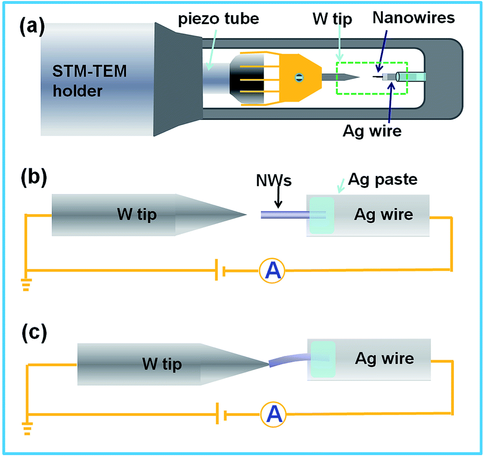 | ||
| Fig. 1 Schematic diagram of the experimental setup and process showing (a) the STM-TEM holder, (b) an enlarged schematic diagram of the dashed area in (a) and (c) a demonstration of the deformation process via controlling the movable W tip. | ||
In our experiment, ZnO NWs prepared by a simple chemical vapor-deposition method were used.23,24 Ar was used as the plasma forming gas, O2 was the reactive gas, and metal zinc powder (99.99% purity) vaporized by cylinder hollow-cathode discharge (HCD) acted as the zinc source. Fig. 2 shows the morphology and structure of the ZnO NWs. Fig. 2(a) is an SEM image showing that the diameters of the ZnO NWs range from 100 nm to 800 nm and the lengths are several tens of microns. These NWs were distributed on a silver wire to conveniently perform the in situ electrical measurements. Fig. 2(b–d) give the detailed structural information via TEM. Fig. 2(b) is a low magnification TEM image showing an individual ZnO NW with a diameter of approximately 160 nm. Fig. 2(c) is the corresponding selected area electron diffraction (SAED) pattern, revealing that the growth is in the [0001] direction. Fig. 2(d) is a high resolution TEM image taken from the white framed region of Fig. 2(b), showing highly crystalline quality.
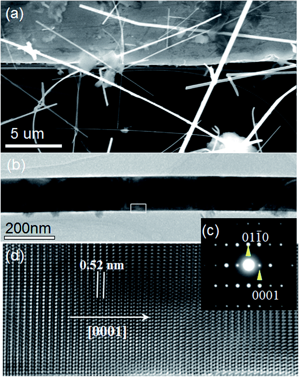 | ||
| Fig. 2 ZnO morphologies. (a) SEM image; (b) TEM image of a single ZnO NW; (c) corresponding SAED pattern; (d) HRTEM image taken from the white framed region of (b). | ||
Using the piezo-motor to drive the W tip to contact and compress the ZnO NW bridged on the Ag electrode, the in situ deformation process and the I–V measurements were recorded. The voltages were swept from −5 to 5 V. Fig. 3(a) displays five sequential TEM images of a typical bending process of an individual ZnO NW and Fig. 3(b) provides the five corresponding I–V curves. It can be observed that the I–V curves show asymmetrical characteristics because of the different electrodes (one electrode is Ag, the other is W).25 Black curve 1 in Fig. 3(b) represents the initial state corresponding to image 1 in Fig. 3(a), whereas the sky-blue curve 5 is the final state corresponding to image 5. From these curves, the highest conductance is observed for the initial state, which then drops with increasing deformation. It is worth noting that the contact interface of the W electrode is larger than that of the ZnO NW in this case. This contact is thus referred to as “full contact” (FC). Fig. 3(c) shows the magnified TEM image of the interface between W and ZnO, which is in accordance with previous reports.15,16
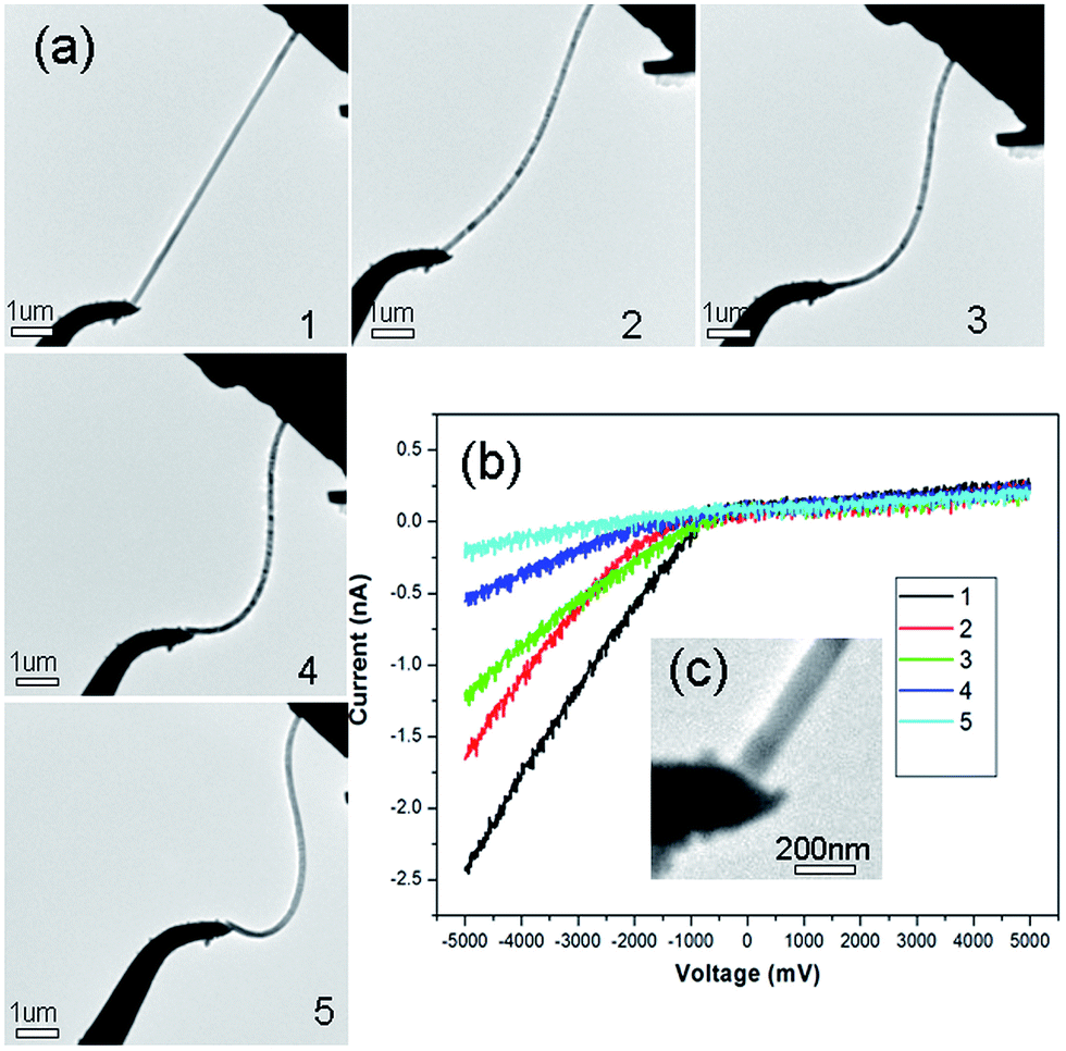 | ||
| Fig. 3 One electrical response induced by the full contact mode. (a) Sequential TEM images of the five typical bending cases of the individual ZnO NW and (b) the corresponding I–V curves for the five states. (c) Magnified TEM image showing the contact between the W tip and the ZnO NW. | ||
However, an inverse electrical response was observed upon changing the contact position of the W tip during the same bending process for the same ZnO NW. Fig. 3(a) provides a series of low magnification TEM images showing the bending process with the corresponding I–V curves for the different bending states shown in Fig. 3(b). Fig. 3(c) is a high magnification TEM image exhibiting the contact between the W tip and the ZnO NW. From this image, the W tip appears very sharp and the contact of the tip is at the center of the end of the nanowire. This contact mode is thus referred to as “point contact” (PC). Eight I–V curves show the change of conductance during the bending process induced by the compressive stress. The black I–V curve indicates the lowest conductance, which corresponds to the initial measurement. With the increase in bending, the conductance was gradually enhanced in this contact mode. This electrical response is contrary to that observed in the above experiment for the same ZnO NW. These two inverse electrical responses were also verified by testing another individual ZnO NW.
Next, we attempted to understand the inverse results of the same ZnO NW during the two bending processes. When comparing the two experiments, all conditions were identical except for the contact mode utilized. Therefore, we then tried to understand the physical processes of these modes. We know that ZnO has semiconducting and piezoelectric properties; thus, two characters may be activated when stress is applied to ZnO. First, as a semiconductor material, stress can change the band structure, carrier effective mass, and motility,26–28 which will significantly affect its electronic transport properties (piezeoresistive effect). For n-type ZnO NWs, tensile strain and compressive strain can narrow and widen the band gap, respectively.14,24 A narrowed band gap would increase the concentration of lighter carriers and ultimately enhance the carrier mobility, finally resulting in conductance enhancement. On the contrary, a widened band gap would cause a reduction in the carrier mobility and conductance. Recent theoretical results have shown that the band gap decreases with increasing bending strain via first-principle studies.29 Thus, in our two cases, the conductance should be improved upon application of the bending strain if only considering the piezoresistive effect.
However, in a polar material, the strain can simultaneously induce a piezoelectric effect. Once deformed by an external force, F, a piezo-electric potential is formed across the bent ZnO NW.5 The stretched side possesses a positive potential, V+, whereas the compressed side exhibits a negative potential, V−.25 Furthermore, the piezoelectric potential induced by the strain will affect the transport properties.30 Some of the free electrons in n-type ZnO NW may be trapped at the surface of the positive side and become non-mobile charges, which lower the effective carrier density in the NW, resulting in an increase in resistance.16 The potential difference is maintained unless the deformation is released or foreign free charges are injected.
Fig. 3(c) shows the first deformation mode. In this case, the W tip and the ZnO NW are in full contact at the initial time. With the increase of bending deformation, the W tip slipped to the tensile side (observed in Fig. 3). Referring to the literatures (ref. 5 and 31), when the probe pushes a NW and bends it, a positive potential is produced at the stretched side of the NW because of the piezoelectric effect. As a result, a potential barrier is produced at the interface between the tip and the NW with the NW being at the higher potential. Such an energy barrier may effectively serve as a p–n junction barrier at the interface that resists the current flow from the tip to the NW. The magnitude of the barrier increases with the increase of the degree of NW bending, resulting in a drastic increase of the rectifying effect. Thus, the transport properties will be reduced by the piezoelectric effect in this case. However, because the contact position between the W tip and the end of the ZnO NW is near the center of the NW (shown in Fig. 4(c)), the metal–semiconductor (M–S) interface may possibly serve as a positively biased Schottky diode. The flow of the free electrons from the loop through the NW to the tip will neutralize the ionic charges distributed in the volume of the NW. The polar charges produced by the displaced Zn2+ and O2− ions caused by the PZ effect are immediately neutralized by external free charges as soon as they are produced by the deformation.5 Thus, the variation of the transport properties that result from the piezoelectric effect can be neglected in this case.
 | ||
| Fig. 4 Inverse electrical response induced by the PC mode. (a) Sequential TEM images of the eight typical bending cases of the same individual ZnO NW, and (b) the corresponding I–V curves for each state. (c) Magnified TEM image showing the contact between the W tip and the ZnO NW. | ||
By combining the piezoresistive and piezoelectric effects, the current would decrease upon increasing the bending deformation under the full contact mode, whereas it would increase upon increasing the bending deformation under the point contact mode because of the negligible piezoelectric effect.
In summary, we performed in situ manipulation and electrical transport measurements on individual ZnO NWs by using a piezo-driven holder inside a transmission electron microscope. By simply adjusting the contact mode, two opposite electrical responses were obtained during the bending process. When the interface of the metal tip fully covered the NW interface, a potential barrier was produced at the interface between the tip and the NW as the bending deformation was increased (the W tip slipped to the tensile side). The current was subsequently reduced because of the coupling of piezoelectric and semiconducting effects. However, when the metal tip only contacted the center of the metal–semiconductor interface, the polar charges resulting from the piezoelectric effect were immediately neutralized because of the conducting channel. In this case, there was no piezoelectric effect but rather the current increased because of the narrowed band gap induced by the bending stress. Exploiting this unique behavior may lead to the development of new nanodevices in the near future.
Acknowledgements
This work was supported by the National Natural Science Foundation of China (11374029), a Foundation for the Author of National Excellent Doctoral Dissertation of PR China (201214), Beijing Nova Program (Z121103002512017), the Key Project of National Natural Science Foundation of China (11234011), Henry Fok of the Ministry of Education Fund (141008), Beijing City Board of Education Project (KM201310005009).Notes and references
- R. F. Service, Science, 1997, 276, 895 CrossRef CAS.
- Z. L. Wang, Mater. Sci. Eng., R, 2009, 64, 33 CrossRef PubMed.
- S. Y. Yang, D. Prendergast and J. B. Neaton, Nano Lett., 2010, 10, 3156 CrossRef CAS PubMed.
- Z. L. Wang, J. Phys.: Condens. Matter, 2004, 16, 829 CrossRef.
- Z. L. Wang and J. H. Song, Science, 2006, 312, 242 CrossRef CAS PubMed.
- X. D. Wang, J. H. Song, J. Liu and Z. L. Wang, Science, 2007, 316, 102 CrossRef CAS PubMed.
- Y. Wang, X. D. Qin and Z. L. Wang, Nature, 2008, 451, 809 CrossRef PubMed.
- J. Zhou, Y. D. Gu, P. Fei, W. J. Mai, Y. F. Gao, R. S. Yang, G. Bao and Z. L. Wang, Nano Lett., 2008, 8, 3035 CrossRef CAS PubMed.
- J. H. He, C. L. Hsin, J. Liu, L. J. Chen and Z. L. Wang, Adv. Mater., 2007, 19, 781 CrossRef PubMed.
- Y. F. Hu, Y. L. Chang, P. Fei, R. L. Snyder and Z. L. Wang, ACS Nano, 2010, 4, 1234 CrossRef CAS PubMed.
- R. W. Shao, K. Zheng, B. Wei, Y. F. Zhang, Y. J. Li, X. D. Han, Z. Zhang and J. Zou, Nanoscale, 2014, 6, 4936 RSC.
- A. Asthana, H. A. Ardakani, Y. K. Yap and R. S. Yassar, J. Mater. Chem. C, 2014, 2, 3995 RSC.
- R. Y. Zhang, H. Andersson, M. Olsen, M. Hummelgård, S. Edvardsson, H. E. Nilsson and H. Olin, Nano Energy, 2014, 3, 10 CrossRef CAS PubMed.
- X. B. Han, G. Y. Jing, X. Z. Zhang, R. M. Ma, X. F. Song, J. Xu, Z. M. Liao, N. Wang and D. P. Yu, Nano Res., 2009, 2, 553 CrossRef CAS.
- P. Gao, Z. Z. Wang, K. H. Liu, Z. Xu, W. L. Wang, X. D. Bai and E. G. Wang, J. Mater. Chem., 2009, 19, 1002 RSC.
- X. D. Wang, J. Zhou, J. H. Song, J. Liu, N. S. Xu and Z. L. Wang, Nano Lett., 2006, 6, 2768 CrossRef CAS PubMed.
- R. Zhu and R. S. Yang, Nanotechnology, 2014, 25, 345702 CrossRef PubMed.
- K. H. Liu, P. Gao, Z. Xu, X. D. Bai and E. G. Wang, Appl. Phys. Lett., 2008, 92, 213105 CrossRef PubMed.
- X. Lin, X. B. He, T. Z. Yang, W. Guo, D. X. Shi, H. J. Gao, D. D. Ma, S. T. Lee, F. Liu and X. C. Xie, Appl. Phys. Lett., 2006, 89, 043103 CrossRef PubMed.
- K. Zheng, R. W. Shao, Q. S. Deng, Y. F. Zhang, Y. J. Li, X. D. Han, Z. Zhang and J. Zou, Appl. Phys. Lett., 2014, 104, 013111 CrossRef PubMed.
- J. J. Wang, R. W. Shao, Q. S. Deng and K. Zheng, Acta Phys. Sin., 2014, 63, 117303 Search PubMed.
- R. W. Shao, K. Zheng, Y. F. Zhang, Y. J. Li, Z. Zhang and X. D. Han, Appl. Phys. Lett., 2012, 101, 233109 CrossRef PubMed.
- L. H. Wang, X. D. Han, Y. F. Zhang, K. Zheng, P. Liu and Z. Zhang, Acta Mater., 2011, 59, 651 CrossRef CAS PubMed.
- B. Wei, K. Zheng, Y. Ji, Y. F. Zhang, Z. Zhang and X. D. Han, Nano Lett., 2012, 12, 4595 CrossRef CAS PubMed.
- J. H. Song, J. Zhou and Z. L. Wang, Nano Lett., 2006, 6, 1656 CrossRef CAS PubMed.
- J. X. Cao, X. G. Gong and R. Q. Wu, Phys. Rev. B: Condens. Matter Mater. Phys., 2007, 75, 233302 CrossRef.
- P. W. Leu, A. Svizhenko and K. Cho, Phys. Rev. B: Condens. Matter Mater. Phys., 2008, 77, 235305 CrossRef.
- P. Neuzil, C. C. Wong and J. Rebound, Nano Lett., 2010, 10, 1248 CrossRef CAS PubMed.
- Z. Y. Gao, J. Zhou, Y. D. Gu, P. Fei, Y. Hao, G. Bao and Z. L. Wang, J. Appl. Phys., 2009, 105, 113707 CrossRef PubMed.
- W. A. Adeagbo, S. Thomas, S. K. Nayak, A. Ernst and W. Hergert, Phys. Rev. B: Condens. Matter Mater. Phys., 2014, 89, 195135 CrossRef.
- Z. L. Wang, Adv. Mater., 2007, 19, 889 CrossRef CAS PubMed.
| This journal is © The Royal Society of Chemistry 2015 |