
 Open Access Article
 This Open Access Article is licensed under a Creative Commons Attribution-Non Commercial 3.0 Unported Licence
3D-printed Cu2O photoelectrodes for photoelectrochemical water splitting†
Jinhyuck
Ahn‡
ab,
Sanghyeon
Lee‡
c,
Jung Hyun
Kim
ab,
Muhammad
Wajahat
ab,
Ho Hyung
Sim
ab,
Jongcheon
Bae
ad,
Jaeyeon
Pyo
a,
Muhammad
Jahandar
 e,
Dong Chan
Lim
e and
Seung Kwon
Seol
*ab
e,
Dong Chan
Lim
e and
Seung Kwon
Seol
*ab
aNano Hybrid Technology Research Center, Korea Electrotechnology Research Institute (KERI), Changwon-si, Gyeongsangnam-do 51543, Republic of Korea. E-mail: skseol@keri.re.kr; Fax: +82-55-280-1590; Tel: +82-55-280-1462
bElectrical Functionality Material Engineering, University of Science and Technology (UST), Changwon-si, Gyeongsangnam-do 51543, Republic of Korea
cDepartment of Mechanical Engineering, The University of Hong Kong, Pokfulam Road, Hong Kong, China
dSchool of Materials Science and Engineering, Pusan National University, Busan, Republic of Korea
eSurface Technology Division, Korea Institute of Materials Science (KIMS), Changwon-si, Gyeongsangnam-do 51508, Republic of Korea
First published on 7th September 2020
Abstract
Photoelectrochemical (PEC) water splitting is an alternative to fossil fuel combustion involving the generation of renewable hydrogen without environmental pollution or greenhouse gas emissions. Cuprous oxide (Cu2O) is a promising semiconducting material for the simple reduction of hydrogen from water, in which the conduction band edge is slightly negative compared to the water reduction potential. However, the solar-to-hydrogen conversion efficiency of Cu2O is lower than the theoretical value due to a short carrier-diffusion length under the effective light absorption depth. Thus, increasing light absorption in the electrode–electrolyte interfacial layer of a Cu2O photoelectrode can enhance PEC performance. In this study, a Cu2O 3D photoelectrode comprised of pyramid arrays was fabricated using a two-step method involving direct-ink-writing of graphene structures. This was followed by the electrodeposition of a Cu current-collecting layer and a p–n homojunction Cu2O photocatalyst layer onto the printed structures. The performance for PEC water splitting was enhanced by increasing the total light absorption area (Aa) of the photoelectrode via controlling the electrode topography. The 3D photoelectrode (Aa = 3.2 cm2) printed on the substrate area of 1.0 cm2 exhibited a photocurrent (Iph) of −3.01 mA at 0.02 V (vs. RHE), which is approximately three times higher than that of a planar photoelectrode with an Aa = 1.0 cm2 (Iph = −0.91 mA). Our 3D printing strategy provides a flexible approach for the design and the fabrication of highly efficient PEC photoelectrodes.
1. Introduction
Unlike fossil fuels, hydrogen is a clean fuel that, when consumed in a fuel cell, produces only water, electricity, and heat.1 Hydrogen can be produced by several methods, such as natural gas reforming, biological processes, and electrolysis.2,3 Currently, most hydrogen is generated worldwide by natural gas steam-reforming, which is an important technology that employs high temperatures (700–1000 °C) and high pressures (300–2500 kPa) to produce hydrogen from natural gas.4,5 Although this method is efficient, excessive fossil fuel and electricity energy consumption in the process can lead to environmental pollution and greenhouse gas emissions.6Hydrogen generation from the separation of water into oxygen and hydrogen by electrolysis using renewable resources of electricity can solve these issues.1–3,7,8 The photoelectrochemical (PEC) water splitting process is the most promising method of producing renewable hydrogen without greenhouse gas emissions. In the PEC water splitting process, hydrogen is produced using sunlight and specialized semiconductors in a water-based electrolyte. The semiconducting materials convert solar energy directly to chemical energy in the form of hydrogen; the minority charge carriers (electrons and holes for p-type and n-type semiconductors, respectively) generated through light absorption by the semiconductor are driven into the solution by the electric field at the junction, where they drive redox reactions such as the hydrogen evolution reaction (HER) on the cathode or the oxygen evolution reaction (OER) on the anode.9–12
Cuprous oxide (Cu2O), an attractive photocathode material, is an intrinsic p-type semiconductor with a direct band gap of 2.0–2.2 eV. The conduction band (ECB = −1.4 eV) of Cu2O is slightly negative compared to the water reduction potential required to reduce hydrogen from water.13–15 Under air mass (AM) 1.5 conditions (1.5 atmospheric thickness), Cu2O has a theoretical photocurrent density (Jph) of 14.7 mA cm−2 and a solar-to-hydrogen conversion efficiency of 18%.16,17 However, the conversion efficiency of Cu2O is lower than its theoretical value due to the short diffusion length (20–100 nm) of the minority carriers in the Cu2O photoelectrode at an effective light absorption depth (∼10 μm).17–20 Therefore, to improve the performance of hydrogen generation during the PEC water splitting process, one effective approach is to increase the total dose of light absorption in the electrode–electrolyte interfacial layer by using a three-dimensional (3D) geometrical photoelectrode.17,21–27
3D printing, also known as additive manufacturing, is a promising method for creating complex 3D objects with large surface-to-volume ratios. As such, it has been used for various electronic applications that require functional components with large surface areas.28–31 Recently, research groups have fabricated PEC 3D electrodes using a selective laser sintering (SLS) 3D printing approach, which uses high energy to sinter metallic powders. First, 3D metallic collectors were produced using the SLS method. Catalytically active layers (IrO2 or TiO2) were deposited on the 3D-printed collectors by thermal processing or electrodeposition.32,33 However, in SLS, it is difficult to reduce the sizes of the printed structures to a micron scale or to use light-weight and flexible polymeric substrates that can be damaged by heat.
In this study, we successfully fabricated the first Cu2O 3D photoelectrode with a large surface-to-volume ratio for PEC water splitting using an extrusion-based 3D printing approach with functional ink at room temperature. Our approach consisted of two steps: (i) direct-ink-writing of graphene 3D structures and (ii) successive electrodeposition of Cu (current collecting layer) and p–n homojunction Cu2O (photocatalyst layer) onto the printed graphene structures. The relatively large light absorption area (Aa) of the 3D photoelectrode increases the activation sites for carrier generation under chopped-light illumination, resulting in a larger photocurrent. The 3D pyramid-shaped photoelectrode (Aa = 3.2 cm2) printed on the substrate area of 1.0 cm2 exhibits Iph values of −3.01 mA at 0.02 V (vs. RHE), which is approximately three times higher than that of a planar photoelectrode with an Aa = 1.0 cm2 (Iph = −0.91 mA).
2. Experimental
Preparation of graphene ink
The graphene ink was prepared by mixing graphene microflakes (0.5 g; Graphene Supermarket) and ethyl cellulose (0.2 g, Sigma-Aldrich, assay 47.5–49.5%) in a mixed solvent composed of toluene (0.65 g, Sigma-Aldrich, ≤99.9%) and xylene (0.65 g, Sigma-Aldrich, ≤98.5%) with a mixer (ARE-310; THINKY Cor.). The rheological properties of the ink were characterized using a rheometer (MCR102, Anton Paar) with a parallel-plate geometry configuration. A stress sweep at a constant frequency of 1 Hz was also performed to record variations in the storage (G′) and loss (G′′) moduli of the ink as a function of sweep stress.3D printing of graphene pyramids
Extrusion-based 3D printing of the graphene pyramids was conducted using a fluid dispenser (Ultimus V, EFD Inc.). The ink was packed into a syringe (3 mL barrel, EFD Inc.) and extruded through a micronozzle (nozzle inner diameter (ID) = 100 μm) under an applied pressure (Pa = 50 psi). The micronozzle position was accurately controlled using three-axis stepping motors. The nozzle motion corresponding to the printed paths was determined using parameterized G-code scripts converted from the designed 3D model. The printing process was observed in situ using an optical monitoring system consisting of an optical lens (10×) and a charge-coupled device camera. Cu foil (thickness: ∼20 μm) was used as the substrate. For electrodeposition of Cu and Cu2O layers, an insulation tape was attached to expose a substrate area of 1.0 cm2 and graphene pyramids were printed on the exposed area.Electrodeposition of Cu and Cu2O layers
A Cu current collecting layer was deposited on the graphene surface at −0.4 V (vs. Ag/AgCl) in an electrolyte composed of 0.5 M CuSO4·5H2O and 0.8 M H2SO4 for 30 min. The deposition temperature was maintained at 25 °C. The p-type Cu2O (photocatalyst layer) was deposited on the surface of the graphene/Cu at −0.3 V (vs. Ag/AgCl) in electrolyte (0.4 M CuSO4·5H2O and 3.0 M sodium lactate) at a pH of 12 for 30 min (deposition temperature: 60 °C). The n-type Cu2O layer for the p–n homojunction was deposited on the surface of the graphene/Cu/p-type Cu2O at 0.02 V (vs. Ag/AgCl) in electrolyte (0.02 M copper acetate and 0.08 M acetic acid) at a pH of 4.9 for 10 min (deposition temperature: 70 °C). The pH of the plating bath was adjusted by adding NaOH. Electrodeposition was performed using a potentiostat (COMPACTSTAT, IVIUM TECHNOLOGIES). The platinum plate was used as the counter electrode and the deposition temperature was maintained using a circulating chiller (DHJF-2005, Zhengzhou Greatwall Scientific Industrial and Trade Co., Ltd).Characterization of photoelectrodes
Morphological changes to the surface of the photoelectrodes during each fabrication step were analyzed using a field-emission scanning electron microscopy (FE-SEM, S4800, Hitachi). The crystalline structure was characterized using an X-ray diffractometer (XRD, Rigaku, D/MAX-2500/PC). The electrode resistance was determined from current–voltage sweep curves obtained using a two-probe system (Keithley 2612A instrument). The PEC performance and Mott–Schottky (M–S) plots of the photoelectrodes with a Cu/p-type Cu2O layer and a Cu/p–n homojunction Cu2O layer were measured in a 0.5 M NaSO4 electrolyte with a three-electrode configuration consisting of an Ag/AgCl electrode (reference), a platinum plate (counter), and a photoelectrode (working). The photoelectrodes were illuminated using an AM 1.5 solar simulator (Sun 2000, Xe lamp, Abet Technologies). The light intensity was calibrated to 100 mW cm−2 using a calibrated silicon detector. Photocurrent transients as a function of the applied potential were recorded by chopped-light illumination (20 s dark and 20 s light). M–S plots were obtained at a fixed frequency of 103 Hz. All potentials were converted to reference with the reversible hydrogen electrode (RHE). In addition, a 150 W Xe lamp equipped with a monochromator was used as the monochromatic excitation light source to carry out the incident photon-to-electron conversion efficiency (IPCE) measurement. UV-vis absorption spectra of the photoelectrode were recorded using a spectrophotometer (Cary 5000, Agilent Technologies).3. Results and discussion
Fig. 1a illustrates the fabrication of the 3D photoelectrode, comprising pyramid arrays, by a sequential process including extrusion-based 3D printing and electrodeposition, i.e., consisting of (i) direct-ink-writing of graphene 3D pyramids and (ii) electrodeposition of Cu and p–n homojunction Cu2O on the printed pyramids. The extrusion-based 3D printing approach requires ink with specific rheological (exhibiting transitions between solid-like and fluid-like behaviors with respect to the applied shear stress) and viscoelastic properties to facilitate the extrusion of the ink through a nozzle under applied pressure.34–36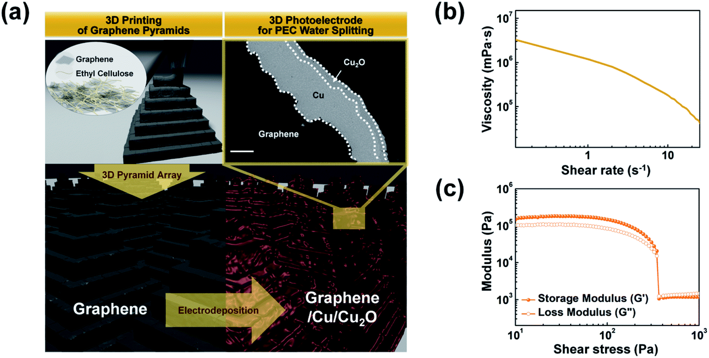 | ||
| Fig. 1 (a) Schematic illustration of the fabrication process of 3D-printed photoelectrodes for water splitting via two successive steps: 3D printing of a pyramid array using graphene ink and functionalization via electrodeposition (Cu and Cu2O layers). Scale bar is 20 μm. (b) Viscosity vs. shear rate and (c) storage (G′) and loss (G′′) moduli vs. ink shear stress. During the printing process, the graphene ink transitions from a solid-like fluid to a liquid-like fluid as a function of the shear stress. | ||
The layer-by-layer printed pyramids with a base length (Lb) of 490 μm and a height (hp) of 365 μm were obtained by successive horizontal and vertical movements of the nozzle (ID = 100 μm). The nozzle was filled with the graphene ink (25 wt% graphene flake and 10 wt% ethyl cellulose (EC) dispersed in a 65 wt% organic solvent mixed with toluene and xylene in the same proportions) and moved by applying a pressure of 50 psi (Video S1 in ESI†). Graphene flakes (average size: ∼7 μm) in the ink served as the conducting and supporting components. The EC acted both as a rheological modifier for continuous ink dispensing and as a binder for maintaining the shape of the printed graphene object during printing (Video S2 in ESI†). The PEC function on the printed structures was assigned by the following simple electrodeposition process: the Cu (layer thickness (T) = 20 μm) current collecting layer and the p–n homojunction Cu2O (T = 5 μm) photocatalyst layer were deposited on the printed pyramids (see FE-SEM image in Fig. 1a for a cross-section of the pyramid electrode). During electrodeposition, the EC also acted as a dissolution inhibitor of the printed graphene object due to its hydrophobic property.
Fig. 1b shows the graphene ink viscosity as a function of the shear rate. The ink had a viscosity (η) of 1.79 × 10⁵ mPa s (at a shear rate of 1 s−1) and exhibited clear shear thinning behavior. The storage (G′) and loss (G′′) moduli of the ink are shown in Fig. 1c. The ink exhibited rheological properties with transitions (shear yield stress = 350 Pa) between solid-like (G′ > G′′) and fluid-like (G′ < G′′) behaviors with respect to the applied shear stress. In an extrusion-based 3D printing approach, such rheological properties ensured a continuous supply of the ink through the micronozzle and maintained the shape of the printed structure, enabling the fabrication of 3D graphene structures.34–36
First, we demonstrated a 3D photoelectrode with a p-type Cu2O photocatalyst layer, which was fabricated by printing 400 graphene pyramids (Lb = 450 μm and hp = 390 μm) followed by successive electrodeposition of Cu and p-type Cu2O layers (Fig. 2). After Cu electrodeposition onto the printed graphene pyramids (i), an area containing dominantly agglomerates of Cu grains and some crystalline structures was observed (ii). The crystallinity of the printed graphene and deposited Cu was confirmed by XRD analyses (Fig. S1 in ESI†). The p-type Cu2O (iii) deposited at −0.3 V (vs. Ag/AgCl) in electrolyte (0.4 M CuSO4·5H2O and 3.0 M sodium lactate) at a pH of 12 exhibited an octahedral morphology because of the increased concentration of hydroxyl ions, which promoted the growth of the (110) and (111) faces to the (100) face.37 The XRD patterns of the p-type Cu2O layer confirmed the presence of the (111), (200), (211), (220), and (310) planes. The change in the resistance of the 3D photoelectrode with respect to the fabrication progress is shown in Fig. 2b. After Cu electrodeposition (current efficiency of electrodeposition: 80.07%, Fig. S2 in ESI†), the resistance decreased to 1.58 Ω, which is similar to that of typical Cu foil (20 μm thickness) (Fig. S3 in ESI†). This indicates that the electrodeposited Cu layer is a suitable current collecting layer for the 3D photoelectrode. The I–V curve of the 3D electrode exhibited an ohmic contact between the Cu layer and the p-type Cu2O layer due to the high work function of Cu (inset of Fig. 2b).38 This led to an accelerated transfer of electrons (and holes) under the electric field, improving the PEC performance of the photoelectrode.39Fig. 2c shows an M–S plot of the fabricated 3D electrode. The negative slope of the linear fit implies that the deposited Cu2O layer is a p-type semiconductor with a flat band potential (Vfb) of 0.58 V vs. a reversible hydrogen electrode (RHE).40,41Fig. 2d shows the PEC performance (photocurrent, Iph) of the 3D photoelectrode as a function of the applied potential (vs. RHE) under chopped-light illumination. As the applied potential increased, the Iph value, which was generated by the chemical reduction of protons and induced photoelectrons, also increased. The spike in Iph observed in the illumination cycle was attributed to pre-adsorbed water molecules on the surface of the 3D photoelectrode.41,42
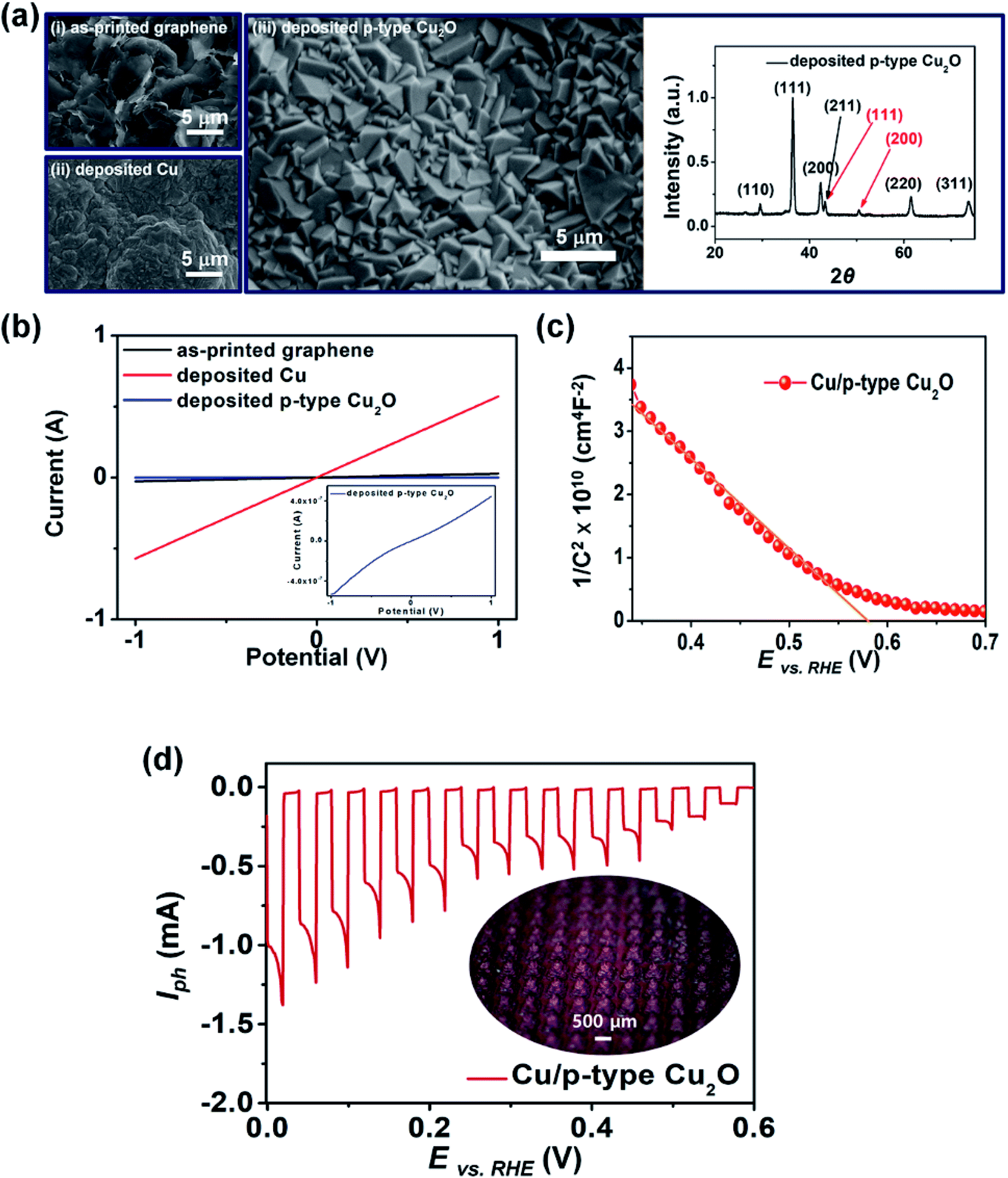 | ||
| Fig. 2 (a) FE-SEM images showing the morphological changes on the surface of the 3D pyramid electrode in each step: (i) as-printed graphene, (ii) deposited Cu layer, and (iii) deposited p-type Cu2O layer. XRD patterns of the deposited Cu/p-type Cu2O layer on the 3D graphene pyramids (red: Cu, black: Cu2O). (b) I–V characteristics of the 3D photoelectrode with respect to the fabrication progress. The inset graph shows an ohmic contact between the Cu and Cu2O after the deposition of p-type Cu2O on the Cu layer. (c) M–S plot of the Cu/p-type Cu2O layer deposited on the 3D graphene pyramids (Vfb = 0.58 V vs. RHE). (d) Chopped-light PEC performance of the 3D photoelectrode as a function of the applied potential (vs. RHE). Inset is an optical image of the 3D photoelectrode composed of 400 pyramids. | ||
To enhance the PEC performance of the 3D pyramid photoelectrode, we adjusted the band gap of the photocatalyst layer by additional deposition of n-type Cu2O, which was achieved by controlling the operating conditions such as the applied potential, solution temperature and pH, electrolyte composition, and additives. Fig. 3a is an FE-SEM image of the n-type Cu2O formed on the surface of the graphene/Cu/p-type Cu2O at an applied potential of 0.02 V (vs. Ag/AgCl) in the electrolyte (0.02 M copper acetate and 0.08 M acetic acid) at a pH of 4.9 for 10 min (deposition temperature: 70 °C). The low concentration of hydroxide ions (OH−) under acidic conditions induced multiple oxygen vacancies in the deposited Cu2O layer, resulting in the deposition of n-type Cu2O.43,44 The morphology of the n-type Cu2O layer exhibited laterally grown polycrystals, in which the crystal growth in the (100) direction was more dominant than in other directions such as (110) and (111). This was due to the dissolution of the thermodynamically unstable Cu2O surface in the acidic solution.45,46
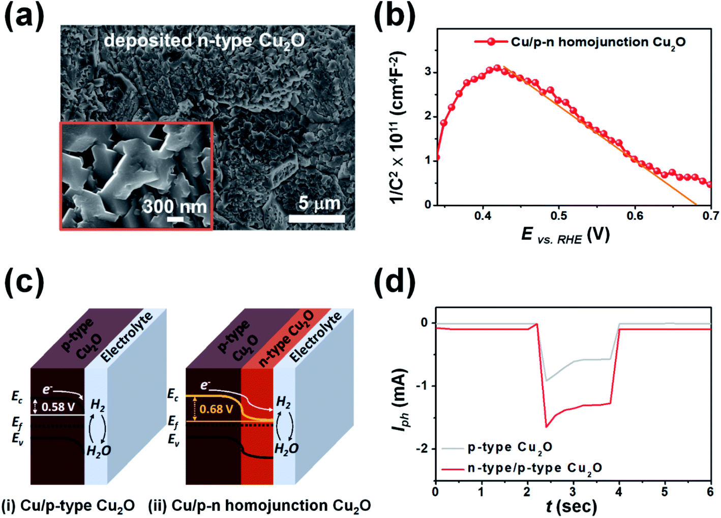 | ||
| Fig. 3 (a) FE-SEM image showing the surface morphology of the n-type Cu2O deposited on the Cu/p-type Cu2O layer of the 3D pyramid photoelectrode. (b) M–S plot of the p–n homojunction Cu2O 3D photoelectrode (Vfb = 0.68 V vs. RHE). (c) Schematic band diagram of (i) Cu/p-type Cu2O (Vfb = 0.58 V) and (ii) Cu/p–n homojunction Cu2O (Vfb = 0.68 V) at equilibrium under dark conditions. (d) Chopped-light PEC performance of the 3D photoelectrode with two different types of photocatalyst layers as a function of time at an applied potential of 0.2 V (vs. RHE). | ||
Fig. 3b shows an M–S plot of the fabricated 3D photoelectrode consisting of Cu (current collecting layer) and a p–n homojunction Cu2O (photocatalyst layer). The multi-linear region is described by two capacitors in series; one corresponding to an n-type Cu2O/electrolyte interface and the other to a p-type Cu2O/n-type Cu2O interface.40,41 The linear fit indicates that the Vfb of the p–n homojunction Cu2O was 0.68 V vs. RHE. The Vfb value was larger than that of the p-type Cu2O due to band-bending formed by upward band-bending of n-type Cu2O and downward band-bending of p-type Cu2O in the depletion region of the p–n junction.47 The p–n homojunction Cu2O resulted in greater splitting of quasi-fermi levels under chopped light illumination, generating a larger Iph than that of p-type Cu2O alone (Fig. 3c).41Fig. 3d shows the PEC performance of the 3D photoelectrode with a p–n homojunction Cu2O and p-type Cu2O as the photocatalyst layer at an applied potential of 0.2 V (vs. RHE) under chopped light illumination (2 s dark and 2 s light). The maximum Iph of the p–n homojunction Cu2O (1.65 mA) is 1.8 times larger than that of the p-type Cu2O (Iph = 0.92 mA). The Iph of the p–n homojunction Cu2O under dark conditions is slightly larger than that of the p-type Cu2O due to enhanced generation of minority carriers in the depletion region of the p–n junction.40,48
We also studied the variations in PEC performance of the p–n homojunction Cu2O photoelectrode due to different shapes, i.e., planar or 3D pyramid, with respect to the total light absorption area (Aa) of the electrode. The 3D photoelectrode consisted of 400 pyramids, each with a fixed Lb of 490 μm, which were printed in close contact without gaps (Fig. 4a). As hp increased to 390, 525, and 650 μm, the Aa values were calculated to increase to 2.45, 2.81, and 3.20 cm2, respectively. As shown in Fig. 4b, increased Aa led to larger Iph values from the photoelectrode under chopped light illumination. The photocurrent density, the UV-vis absorption spectra, and the IPCE of the p–n homojunction Cu2O electrodes with planar and 3D pyramid shapes exhibited similar value due to same photoelectrode configuration (Fig. S4 and S5 in ESI†). Thus, these results were attributed to an increased number of activation sites for photocurrent generation. The Iph of a planar electrode with an Aa of 1 cm2 was 0.91 mA, while the 3D pyramid photoelectrode exhibited 2.35, 2.70, and 3.01 mA at 0.02 V (vs. RHE), as hp increased. These results show that PEC performance can be enhanced through the use of specially designed 3D photoelectrodes.
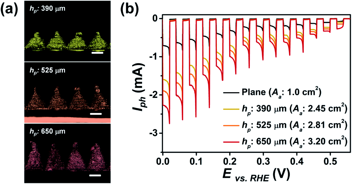 | ||
| Fig. 4 (a) Optical images of the fabricated 3D photoelectrodes composed of 400 pyramids. The total light absorption area (Aa) of the 3D photoelectrodes is modulated by adjusting hp to 390, 525, and 650 μm (fixed Lb: 490 μm). The scale bar is 250 μm. (b) Chopped-light PEC performance of the p–n homojunction Cu2O electrodes with planar and 3D pyramid shapes with respect to the total light absorption area (Aa). | ||
4. Conclusions
We demonstrated the fabrication process for a novel Cu2O 3D photoelectrode with a large total light absorption area (Aa) for PEC water splitting. The fabrication process is a two-step method consisting of direct-ink-writing of graphene pyramid arrays and electrodeposition of a Cu current collecting layer and a p–n homojunction Cu2O photocatalyst layer onto the printed pyramids. The rheological properties of the 3D-printable graphene ink enabled continuous ink extrusion without clogging the nozzle while also retaining the shape of the printed graphene structures. The PEC performance of the 3D photoelectrode was enhanced through two fabrication factors: (i) by adjusting the band gap of the photocatalyst layer using simple electrodeposition and (ii) by increasing the Aa value of the photoelectrode. The deposited p–n homojunction Cu2O resulted in enhanced splitting of quasi-fermi levels under chopped light illumination, inducing greater carrier generation. Increasing the Aa value of the photoelectrode contributed to increased activation sites for carrier generation. As Aa increased, the 3D pyramid photoelectrode with the p–n homojunction Cu2O layer exhibited Iph values of 2.35, 2.70, and 3.01 mA at 0.02 V (vs. RHE) under chopped light illumination of 100 mW. We believe that this method is an effective approach for fabricating diversely shaped 3D photoelectrodes that exhibit high PEC performances. As such, this study is an important advance in PEC water splitting research.Conflicts of interest
There are no conflicts to declare.Acknowledgements
This research was supported in part by Korea Electrotechnology Research Institute (KERI) primary research program (20-12-N0101-23) through the National Research Council of Science & Technology (NST) funded by Ministry of Science and ICT.Notes and references
- T. Bak, J. Nowotny, M. Rekas and C. Sorrell, Int. J. Hydrogen Energy, 2002, 27(10), 991–1022 CrossRef CAS.
- I. Dincer and C. Acar, Int. J. Hydrogen Energy, 2015, 40(34), 11094–11111 CrossRef CAS.
- M. A. K. Lodhi, Int. J. Hydrogen Energy, 1987, 12(7), 461–468 CrossRef CAS.
- A. P. Simpson and A. E. Lutz, Int. J. Hydrogen Energy, 2007, 32(18), 4811–4820 CrossRef CAS.
- L. Q. Nguyen, L. C. Abella, S. M. Gallardo and H. E. Hinode, React. Kinet. Catal. Lett., 2008, 93(2), 227–232 CrossRef CAS.
- M. H. Halabi, M. H. J. M. Croon, J. Schaaf, P. D. Cobden and J. C. Schouten, Appl. Catal., A, 2010, 389(1–2), 68–79 CrossRef CAS.
- T. Hisatomi, J. Kubota and K. Domen, Chem. Soc. Rev., 2014, 43(22), 7520–7535 RSC.
- S. U. M. Khan, M. Al-Shahry and W. B. Ingler Jr, Science, 2002, 297(5590), 2243–2245 CrossRef CAS.
- A. Fujishima and K. Honda, Nature, 1972, 238(5358), 37–38 CrossRef CAS.
- X. Yang, A. Wolcott, G. Wang, A. Sobo, R. C. Fitzmorris, F. Qian, J. Z. Zhang and Y. Li, Nano Lett., 2009, 9(6), 2331–2336 CrossRef CAS.
- V. M. Aroutiounian, V. M. Arakelyan and G. E. Shahnazaryan, Sol. Energy, 2005, 78(5), 581–592 CrossRef CAS.
- Y. Qiu, Z. Pan, H. Chen, D. Ye, L. Guo, Z. Fan and S. Yang, Sci. Bull., 2019, 64, 1348–1380 CrossRef CAS.
- P. E. Jongh, D. Vanmaekelbergh and J. J. Kelly, Chem. Mater., 1999, 11(12), 3512–3517 CrossRef.
- Z. Ai, H. Xiao, T. Mei, J. Liu, L. Zhang, K. Deng and J. Qiu, J. Phys. Chem. C, 2008, 112(31), 11929–11935 CrossRef CAS.
- Z. Zheng, B. Huang, Z. Wang, M. Guo, X. Qin, X. Zhang, P. Wang and Y. Dai, J. Phys. Chem. C, 2009, 113(32), 14448–14453 CrossRef CAS.
- A. Paracchino, V. Laporte, K. Sivula, M. Grӓtzel and E. Thimsen, Nat. Mater., 2011, 10(6), 456–461 CrossRef CAS.
- K. P. Musselman, A. Wisnet, D. C. Iza, H. C. Hesse, C. Scheu, J. L. MacManus-Dricsoll and L. Schmidt-Mende, Adv. Mater., 2010, 22(35), 254–258 CrossRef.
- Z. Zhang, R. Dua, L. Zhang, H. Zhu, H. Zhang and P. Wang, ACS Nano, 2013, 7(2), 1709–1717 CrossRef CAS.
- C. J. Engel, T. A. Polson, J. R. Spado, J. M. Bell and A. Fillinger, J. Electrochem. Soc., 2008, 155(3), 37–42 CrossRef.
- S. Hacialioglu, F. Meng and S. Jin, Chem. Commun., 2012, 48(8), 1174–1176 RSC.
- S. Yoon, J.-H. Lim and B. Yoo, J. Alloys Compd., 2016, 677, 66–71 CrossRef CAS.
- A. Kargar, K. Sun, Y. Jing, C. Choi, H. Jeong, Y. Zhou, K. Madsen, P. Naughton, S. Jin, G. Y. Jung and D. Wang, Nano Lett., 2013, 13(7), 3017–3022 CrossRef CAS.
- K. Sun, Y. Jing, C. Li, X. Zhang, R. Aguinaldo, A. Kargar, K. Madsen, K. Banu, Y. Zhou, Y. Bando, Z. Liu and D. Wang, Nanoscale, 2012, 4(5), 1515–1521 RSC.
- H. Lin, X. Long, Y. An, D. Zhou and S. Yang, Nano Lett., 2019, 19, 455 CrossRef CAS.
- R. Xiong, W. Zhang, Y. Zhang, Y. Zhang, Y. Chen, Y. He and H. Fan, Nanoscale, 2019, 11, 18081 RSC.
- C. Li, Z. Chen, W. Yuan, Q.-H. Xu and C. M. Li, Nanoscale, 2019, 11, 1111–1122 RSC.
- J. Yuan, C. Li, T. Li, M. Jing and W. Yuan, Sol. Energy Mater. Sol. Cells, 2020, 207, 110349 CrossRef CAS.
- C. Zhao, C. Wang, R. Gorkin, S. Beirne, K. Shu and G. G. Wallace, Electrochem. Commun., 2014, 41, 20–23 CrossRef CAS.
- W. S. Chang, J. H. Kim, D. Kim, S. H. Cho and S. K. Seol, Macromol. Chem. Phys., 2014, 215(17), 1633–1638 CrossRef CAS.
- S. D. Lacey, D. J. Kirsch, Y. Li, J. T. Morgenstern, B. C. Zarket, Y. Yao, J. Dai, L. Q. Garcia, B. Liu, T. Gao, S. Xu, S. R. Raghavan, J. W. Connell, Y. Lin and L. Hu, Adv. Mater., 2018, 30(12), 1705651 CrossRef.
- W. Yu, H. Zhou, B. Q. Li and S. Ding, ACS Appl. Mater. Interfaces, 2017, 9(5), 4597–4604 CrossRef CAS.
- A. Ambrosi and M. Pumera, Adv. Funct. Mater., 2018, 28(27), 1700655 CrossRef.
- C.-Y. Lee, A. C. Taylor, S. Beirne and G. G. Wallace, Adv. Energy Mater., 2017, 7(21), 1701060 CrossRef.
- J. H. Kim, S. Lee, M. Wajahat, J. Ahn, J. Pyo, W. S. Chang and S. K. Seol, Nanoscale, 2019, 11(38), 17682 RSC.
- S. Lee, M. Wajahat, J. H. Kim, J. Pyo, W. S. Chang, S. H. Cho, J. T. Kim and S. K. Seol, ACS Appl. Mater. Interfaces, 2019, 11(7), 7123–7130 CrossRef CAS.
- B. G. Compton and J. A. Lewis, Adv. Mater., 2014, 26(34), 5930–5935 CrossRef CAS.
- S. Yoon, M. Kim, I.-S. Kim, J.-H. Lim and B. Yoo, J. Mater. Chem. A, 2014, 2(30), 11621–11627 RSC.
- I. S. Brandt, C. I. L. Araujo, V. Stenger, R. G. Delatorre and A. A. Pasa, ECS Trans., 2008, 14(1), 413–419 CrossRef CAS.
- H. G. Kim, E. D. Jeong, P. H. Borse, S. Jeon, K. Yong, J. S. Lee, W. Li and S. H. Oh, Appl. Phys. Lett., 2006, 89(6), 064103 CrossRef.
- Y. Wang, Z. Lou, W. Niu, Z. Ye and L. Zhu, Nanotechnology, 2018, 29(14), 145402 CrossRef.
- T. Wang, Y. Wei, X. Chang, C. Li, A. Li, S. Liu, J. Zhang and J. Gong, Appl. Catal., B, 2018, 226, 31–37 CrossRef CAS.
- A. W. Maijenburg, M. G. Zoontjes and G. Mul, Electrochim. Acta, 2017, 245, 259–267 CrossRef CAS.
- R. Garuthara and W. Siripala, J. Lumin., 2006, 121(1), 173–178 CrossRef CAS.
- P. Grez, F. Herrera, G. Riveros, A. Ramirez, R. Henriquez, E. Dalchiele and R. Schrebler, Phys. Status Solidi A, 2012, 209(12), 2470–2475 CrossRef CAS.
- C. M. McShane and K.-S. Choi, J. Am. Chem. Soc., 2009, 131(7), 2561–2569 CrossRef CAS.
- W. Zhao, W. Fu, H. Yang, C. Tian, M. Li, Y. Li, L. Zhang, Y. Sui, X. Zhou, H. Chen and G. Zou, CrystEngComm, 2011, 13(8), 2871–2877 RSC.
- B. Lipovšek, F. Smole, M. Topic, I. Humar and A. R. Sinigoj, AIP Adv., 2019, 9(5), 055026 CrossRef.
- G. Heidari, M. Rabani and B. Ramezanzadeh, Int. J. Hydrogen Energy, 2017, 42(15), 9545–9552 CrossRef CAS.
Footnotes |
| † Electronic supplementary information (ESI) available: The supporting Videos S1 and S2 discussed in the manuscript, a brief description of the supporting videos, and supporting figures. See DOI: 10.1039/d0na00512f |
| ‡ These authors contributed equally to this work. |
| This journal is © The Royal Society of Chemistry 2020 |