
 Open Access Article
 This Open Access Article is licensed under a Creative Commons Attribution-Non Commercial 3.0 Unported Licence
Adjustable metal particle grid formed through upward directed solid-state dewetting using silicon nanowires†
Steaphan Mark
Wallace
*ab,
Wipakorn
Jevasuwan
a and
Naoki
Fukata
 *ab
*ab
aInternational Center for Materials Nanoarchitectonics, National Institute for Materials Science, Tsukuba, 305-0044, Japan. E-mail: FUKATA.Naoki@nims.go.jp; Steaphan.wallace@gmail.com
bGraduate School of Pure and Applied Sciences, University of Tsukuba, Tsukuba, 305-8573, Japan
First published on 16th October 2020
Abstract
Sub-micron sized metal particles were formed through the annealing of sputtered metal thin films on silicon nanowires (SiNWs). During high-temperature annealing, the cylindrical SiNW structures induce the solid-state dewetting behavior to consistently move up the SiNW sides and form partial-spherical particles with uniform sizes on the nanowire tops. By adjusting the size parameters of the SiNW substrate and the metal thin film, the particles can be adjusted in size and layout along an array. This contrasts with the random dewetted particles seen on planar surfaces, and known movement towards pitted nanostructures. Ag, Au, Cu, and Ni have shown equivalent particle formation behavior and some alloying is also shown to be possible. These results open a path for a well-controlled and consistent method of metal particle formation at the nano to micro-scale and offer some insight on metal particle dewetting mechanisms. Suggested applications for the resulting regular particle grids include plasmonic sensors such as SERS.
Introduction
Metal particles engineered at the nanoscale have a great number of uses and have been researched intensively for many years. It is not difficult to make metal particles, but the control and consistency of the particles is often a challenging aspect, and many bottom-up and top-down procedures exist for forming nanoparticles which result in a broad range of sizes.1–5 Where progress has been made in achieving constant shape and size of particles, they are often either colloidal or randomly located on a surface.6,7 This is not suitable for device applications which work best with finely controlled particle orientation and their combination with nano-architecture substrates.8–11For the purpose of controlling metal particles on a substrate surface, there has been a swell of interest in metal thin film dewetting and particle migration behavior.12–15 It is known that solid-state dewetting of metal thin films occurs at temperatures much lower than the metal's bulk melting temperature, which depends greatly on the metal thin film thickness.16 At high temperature, metal thin films will quickly dewet from passive surfaces and contract in order to reduce the film's surface energy, exposing the underlying surface.17 If the thin film is sufficiently thin and annealed long enough, the film may cross the percolation threshold to form isolated island particles.18 These particles will sometimes migrate randomly on the surface and merge with other particles, resulting in randomly sized and placed particles on a flat surface.19,20 However, if the surface has been shaped, the dewetting and migration of the metal can be altered according to the effect that the substrate has on the surface energy of the particle.21,22 These effects can be used for engineering the formation and placement of metal particles on the target surface for application. For instance, the nano-pit method of fabrication relies on the dewetting tendency to move away from convex surfaces and towards concave surfaces which cradle the particles.23,24 Uniform particle grids have already been produced in this way but this technique limits the substrate to shallow pits which can be easily disrupted by different deposition thicknesses. Detailing of alternate solid-state dewetting tendencies is needed for expanding the field and for the inclusion of other substrate structures.
Through our group's work with silicon nanowires (SiNWs),25–27 it was observed that metal thin films will easily form particles on the top of cylindrical nanowires. This was suspected to be due to the SiNW surface geometry's effect on the metal thin film surface energy. It was hypothesized that adjusting the SiNW parameters would lead to a high degree of control over the formation of metal particles on the nanowire tops. Though metal particles on nanowire structures are commonly grown in the reverse process,28,29 by depositing particles on a flat surface and then etching or growing the nanowires underneath, control and consistency of the particle/nanowire placement and size is difficult and the type of metal particle is limited by the growth or etching reactions. In contrast, the particle grown from SiNW technique seen here is unique in its solid-state dewetting process, its resulting quality, and its capability to use many metals. We sought to better understand this process and conducted an examination of the conditions at which different metals will form particles on top of SiNWs. The resultant particles were then characterized for their structural properties.
Experimental
SiNWs were prepared by a regular nanoimprint lithography method.30,31 UV photoresist was spin-coated onto n-Si(100) wafers and imprinted by a quartz mold to form a nanohole array. The imprinted resist is used to deposit MgO disks by an electron-gun evaporator onto the Si. Bosch process plasma etching (cycling of 35 sccm SF6 and C4F8 gases in a Sumitomo Silicon Deep RIE machine) vertically removes Si around the disks to form SiNWs. These SiNWs are cylindrically shaped, have straight-edged sides, flat tops, and are surrounded by a flat but roughened base substrate. The diameter and spacing of the SiNWs are controlled by the quartz mold and were ordinarily 200 nm in diameter and spaced 500 nm or 600 nm apart in this experiment. The SiNW length is controlled by the plasma etching parameters where 3.5 min etching resulted in SiNWs 500 nm long.Many metals will react with silicon at high temperature, so a passivating layer was used to separate the metal from the Si substrate. For this purpose, a thin layer of SiO2 was added by thermal oxidation of the sample at 975 °C. The oxidized substrates were cleaned and Ag thin films were deposited onto the substrate by sputtering while rotating the sample. A typical film thickness equivalent to 200 nm when deposited on a planar perpendicular surface (and therefore denoted as 200 nmplanar in this report) was deposited onto the SiNWs. The actual thickness of the thin film differs on the different parts of the SiNW substrate surface. To test the process for other metals and alloys, other samples were deposited with Ni, Au, and Cu instead of, or in combination with, Ag.
The samples were then annealed in a hot-walled quartz tube furnace in an inert atmosphere of 50 sccm Argon at 300 torr at various temperatures and times as explained in the results section. A magnetic transfer rod was used to quickly move the samples between the hot zone and cool zones of the furnace to precisely control the annealing time.
After cooling, the samples were mechanically severed and the cross-sections were characterized by scanning electron microscopy (SEM) to observe their structure and the chemical compositions were recorded by an attached energy-dispersive X-ray spectrometer (EDS). The horizontal particle diameter of some samples was determined by image analysis software for >140 particles. Crystallographic data was gathered using a PANalytical X'Pert thin film X-ray diffractometer (XRD) using Cu Kα radiation and a 5° grazing incidence angle.
Results & discussion
Dewetting behavior on nanowires
Ag thin films on planar surfaces were annealed as controls to illustrate the dewetting process. When metal is deposited as a continuous flat thin film on a planar surface and then annealed, such as Fig. 1(a), the metal dewets if favorable conditions are met. These conditions include a sufficiently thin film, low metal-substrate surface energy, high enough annealing temperature, and time.18 Many metals have weak interactions with SiO2 which leads to strong dewetting behavior.32 In the beginning, when the thin film is heated and the mobility of atoms increases, grain growth occurs and grain boundaries facilitate the nucleation of holes in the film.33 The location of these holes on the film is randomly distributed over the surface. The size of the holes increases and separates the film into sections which contract towards their centers until a stable rounded structure is formed, as illustrated in Fig. 1(d). Thick films may reach equilibrium when still an interconnected, percolated structure as in Fig. 1(b). With suitably thin films and long enough annealing time, the structure will cross the percolation threshold and separate to form spheroid islands such as in Fig. 1(c). | ||
| Fig. 1 Dewetting behavior on planar and SiNW surfaces. (a) 200 nm sputtered Ag film on planar SiO2 surface (b) 200 nm Ag film after annealing at 800 °C showing hole nucleation leading to dewetting. (c) 65 nm Ag film after annealing at the same conditions and dewetting into islands (d) illustration of metal dewetting process on planar surface. Grain boundaries leads to hole nucleation and then isolation into regions that contract into dewetted particles (e) nanoimprint SiNW and oxide film. (f) 200 nmplanar Ag sputtered onto SiNW, showing profile of continuous sputtered thin film. (g) The same sample after 15 second anneal at 800 °C, showing progression of the dewetting process. (h) Illustration of metal dewetting behavior initiating at the thin part of the film at the SiNW sides. The film on the SiNW then migrates up towards the center of mass to form a particle on top. | ||
In this experiment, the cylindrical SiNWs on a flat floor as seen in Fig. 1(e) were used to guide the dewetting process. When the 200 nmplanar Ag metal is sputtered onto the sample while rotated it takes on the shape seen in Fig. 1(f). Due to the nature of the sputtering, the deposition is thicker on top and thinner on the sides of the SiNW. The thickness decreases slightly going down the length of the SiNW and is thinnest near the base but is continuous over the entire SiNW sample. These results appear to be important for initiating dewetting. As the thin film on the sides is thinner, they will dewet quicker than the films on the floor and tops of the SiNWs. The thinnest section near the base facilitates hole nucleation and pinches off the film from the floor. Despite being above the percolation threshold for the equivalent planar film, the film on the SiNW becomes isolated and is similar in mass to the films isolated on the other SiNWs. Once isolated, the metal will migrate upwards to the top as imaged in Fig. 1(g) and illustrated in Fig. 1(h). This upward movement is thought to be a combination of symmetrical contraction towards the thicker and less mobile mass of metal on the top of the SiNW, and a tendency to move away from the curved surface and corners of the SiNW sides. Once the particle has formed on top of the SiNW, the corners will keep the particle pinned to the SiNW top instead of migrating back down. After cooling, the particles become strongly attached to the SiNWs. The effect of gravity is negligible as the same results occur whether the SiNWs point either upwards or downwards during annealing (Fig. S1†). With the proper conditions, this effect should produce particles on nearly every SiNW over the entire sample area. Meanwhile, the material on the floor between the NWs will remain as a thin film if the temperature is below the dewetting point for its particular thickness.
XRD data obtained from the Ag surface (both the particles and underlying Ag) of an annealed sample is shown in Fig. 2(b). A multi-crystalline Ag crystal structure can be seen both before and after annealing with similar peak ratios. More intense and narrow peaks can be seen after annealing due to the increase in crystal grain size compared to the sputtered structure. The annealing also causes only a very slight rightward shift probably due to a small change in residual stress.34
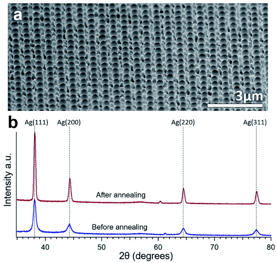 | ||
| Fig. 2 (a) Wide view SEM image of consistent Ag particle formation on NWs over a wide area. (b) XRD spectrum of the surface of the same sample showing Ag crystal peaks before and after annealing. | ||
One important attribute of the sputtering deposition is the continuous coating that is formed. Because the direction of incoming metal is at an angle in a typical sputtering machine, the sample is rotated. If the deposition angle is held at a single direction as in Fig. 3(a) or perpendicular to the sample (Fig. S2†), then the thin film will appear with pores in the film on the side of the SiNW. When annealing, dewetting will initiate at these pores and will lead to small particles on the SiNW sides which will not migrate upward, seen in Fig. 3(b).
 | ||
| Fig. 3 SEM images of samples with alternate unsuccessful conditions (a) Ag sputtered on SiNWs at a sustained angle, with a discontinuous film on the SiNW sides. (b) Same sample after annealing. Minor particles remain on the SiNW side walls. (c) 200 nmplanar of Ag on SiNWs annealed at 700 °C for 2.5 min, dewetting is minimal and incomplete. (d) 200 nmplanar of Ag on SiNWs annealed at 900 °C for 2.5 min, leading to smaller particles, and some substrate damage. (e) 50 nmplanar Ag on 500 nm long SiNWs annealed, resulting in particles dewetting on the floor and SiNW sides. (f) 300 nmplanar Ag on 500 nm long SiNWs annealed, resulting in random particle sizes. (g) Illustration of the effect a change in deposition thickness has on the distance between the top of the SiNW and the top of the thin film on the floor. | ||
Effects of different conditions on dewetting behavior
For application, it is desirable that the dimensions of the metal particles can be controlled and adjusted through the experimental setup. For this purpose, samples annealed at different temperatures, deposition thicknesses, and SiNW dimensions were investigated for the effects on the particle results.To initiate dewetting at a certain thin film thickness, a sufficiently high temperature is needed which corresponds with that thickness. The association between thin film thickness and dewetting temperature for various metals on flat surfaces can be found in other reports.35,36 In the nanowire substrate case, at a temperature slightly below dewetting temperature, grain growth and some hole nucleation may occur but the metal will not form particles, as seen in Fig. 3(c). At temperatures much higher than the dewetting temperature of the entire metal film, the entire film experiences strong dewetting. This will cause hole nucleation between SiNWs and more metal to migrate off the SiNWs, leading to small irregular particles as seen in Fig. 3(d). Overly high temperatures also make it more likely for large particles to touch and merge on the SiNWs or to damage the underlying substrate (Fig. S3†). Consequently, it appears that an annealing temperature above the dewetting temperature of the film on the SiNW sides but below the dewetting temperature of the film on the SiNW top should be used as this will cause the film to consistently dewet off the sides and into stationary particles on top. This temperature will depend on the type of metal and the film thickness found on the different sections of the nanowire. For this experiment, 200 nmplanar of Ag could form proper particles when annealed at 800 °C for 30 seconds or more. Lower temperatures can potentially be used with longer annealing times.
Adjusting the metal deposition thickness had a complex effect on the particle quality. On a planar surface, a thicker film will simply increase the necessary dewetting temperature and form either larger particles or percolated films compared to thinner films. On the SiNW surface, changing the deposition thickness has the added effect of changing the distance from the top of the film on the floor to the top of the SiNW, illustrated in Fig. 3(g). This will change the pinch-off point and therefore the amount of material that will migrate up the SiNWs. At low deposition thicknesses, the deposited film may not be continuous and particles will form on the SiNW walls while the film on the floor dewets into particles as well, such as the 50 nmplanar thick film in Fig. 3(e). At high deposition thicknesses relative to the SiNW height, the film on the floor approaches the SiNW tops and the resulting particles will be small and more random such as the 300 nmplanar thick film in Fig. 3(f). As a result, finding the right deposition thickness relative to the nanowire dimensions is necessary for well-formed particles.
Metal particles could be successfully formed on a variety of sizes of SiNWs. To test the effect of SiNW height, 200 nmplanar Ag was deposited on samples with three different SiNW heights and annealed at the same conditions. The nanowire height was adjusted by using different plasma etching times in the nanoimprint lithography process. Increasing the height of the SiNW while keeping the deposition thickness constant was seen to increase the amount of metal that will travel upward and therefore the size of the particle. Arbitrary heights of 540 nm, 650 nm, and 810 nm caused an increase of the average horizontal particle diameters of 315 nm, 400 nm, and 425 nm respectively which can be seen in the SEM images and particle size distributions of Fig. 4(a–c). This is likely due to the increase of the distance between the floor film and the SiNW top, and an increase of the ratio of the deposited metal on the SiNW sides compared to the floor, depicted in Fig. 4(f). This also reduces the thickness of the metal on the floor, which will also dewet if it approaches thicknesses similar or lower than that on the SiNW walls.
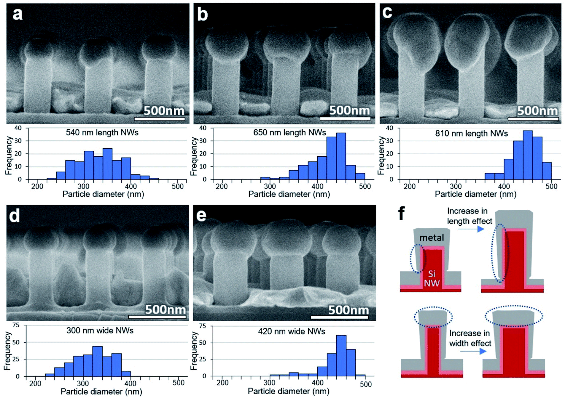 | ||
| Fig. 4 Sample SEM images and particle diameter distribution plots of 200 nmplanar Ag deposited on SiNWs with heights of (a) 540 nm, (b) 650 nm, and (c) 810 nm. The size of the particle increases with the increasing SiNW height. (d) 200 nm diameter SiNWs and (e) 275 nm diameter nanowires with 200 nmplanar Ag depositions. The metal particles on the larger diameter nanowires have proportionally larger diameter metal particles. (f) Illustrations of the how increasing the NW height increases the proportion of metal sputtered onto the sides of the SiNWs that travels upwards with annealing, and how increasing the NW diameter increases the proportion of metal sputtered onto the tops of the SiNW that remains in place with annealing. | ||
Alternatively, to test the effect of SiNW diameter, 200 nmplanar Ag was deposited on SiNWs of different diameters and annealed at the same conditions. Nanowire diameter can be adjusted by the lithography process, or by increasing or decreasing the oxide layer. Changing the SiNW diameter also changed the particle size. 200 nm and 275 nm diameter SiNWs were formed by adjusting the oxide layer and resulted in particles with average horizontal metal particle diameters of 300 nm and 420 nm respectively, seen in Fig. 4(d and e). This is likely due to the amount of metal material deposited on the SiNW tops, depicted in Fig. 4(f).
Although changing the SiNW height and diameter individually could change the size of the metal particles, there are limits on the extent of this process. As already seen in Fig. 3(e), if the volume of metal on top of the SiNW is too small, without reducing the diameter of the SiNW, the metal particle may flatten. And, as seen in Fig. 4(c), if the particle is too massive and the diameter of the SiNW is not wide enough to support the particle's normal wetting surface area then the particle will sag over the SiNW edge, reducing uniformity of the sample. Therefore, large changes in particle size should be made by adjusting both the SiNW height and diameter together.
Other metals and alloying
Particle formation behavior on nanowire tops was observed for all the metals that were tested (Ag, Au, Ni, and Cu). The dewetting behavior was similar among each of the metals on a SiO2 surface. Example SEM images of particles corresponding to each of these metals are shown in Fig. 5(a–d). In this experiment, 200 nmplanar of Ag, Au, and Cu each formed particles at around 800 °C after 2 minutes because of their relatively similar bulk melting temperatures. 200 nmplanar Ni could form particles at around 900 °C after 2 minutes due to its higher bulk melting temperature.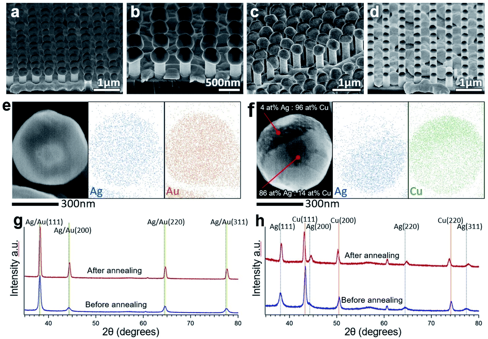 | ||
| Fig. 5 (a) SEM image of 200 nmplanar Ag particle array, (b) 200 nmplanar Ni particle array, (c) 200 nmplanar Cu particle array, and (d) 100 nmplanar Au particle array. (e) SEM image and EDS mapping of alloy particle formed from 100 nmplanar Ag and 100 nmplanar Au depositions. The corresponding EDS maps of Ag and Au show a smooth distribution. (f) Alloy particle formed from 50 nmplanar Ag and 200 nmplanar Cu. The SEM imaging displaying EDS point composition analysis results and EDS maps of Ag and Cu show how the metals are concentrated in different regions. (g) XRD data of the 100 nmplanar Ag on 100 nmplanar Au sample before and after annealing. (h) XRD data of the 50 nmplanar Ag on 200 nmplanar Cu sample showing peak shifts after annealing. | ||
Alloyed nanoparticles are of particular interest because they can combine the properties of individual elements or allow for complex structures.37 To investigate the potential of alloying using this method, Ag and Au were deposited one after the other on SiNW arrays. One sample had 100 nmplanar Au on 100 nmplanar Ag and the second sample had 50 nmplanar Ag on 100 nmplanar Au. Both samples were annealed at 750 °C for 2.5 minutes. SEM-EDS mapping of individual particles showed an even distribution of Au and Ag, such as in Fig. 5(e). EDS spectra from single points showed the calculated atomic ratio of Au![[thin space (1/6-em)]](https://www.rsc.org/images/entities/char_2009.gif) :Ag to be 49:51 for the first sample and 65:35 for the second sample, close to that expected by the deposition thickness. XRD data in Fig. 5(g) shows strong single peaks aligning at the overlapping Ag and Au peaks both before and after annealing along with a decrease in peak width and possible slight rightward peak shift after annealing as also seen in the pure Ag sample. Together, the EDS and XRD data suggest that a good level of controllability can be achieved for forming solid solution alloy metal particles by this method. 50 nmplanar Ag on 200 nmplanar Cu was also tested as these metals do not form a solid solution by annealing. Spherical particles with different textured regions could be seen in SEM. SEM-EDS mapping in Fig. 5(f) and single-point spectra at different locations on the particle suggest that the different regions vary in Ag:Cu composition. XRD from the sample after sputtering reveals peaks aligning well to both Ag and Cu standard peaks. However, after annealing, the Ag peaks shift rightward (from compression) and the Cu peaks shift leftward (from tension). This is likely an adjustment due to the difference in the lattice parameters of the two metals and a sign that there has been alloying of the metals.38
:Ag to be 49:51 for the first sample and 65:35 for the second sample, close to that expected by the deposition thickness. XRD data in Fig. 5(g) shows strong single peaks aligning at the overlapping Ag and Au peaks both before and after annealing along with a decrease in peak width and possible slight rightward peak shift after annealing as also seen in the pure Ag sample. Together, the EDS and XRD data suggest that a good level of controllability can be achieved for forming solid solution alloy metal particles by this method. 50 nmplanar Ag on 200 nmplanar Cu was also tested as these metals do not form a solid solution by annealing. Spherical particles with different textured regions could be seen in SEM. SEM-EDS mapping in Fig. 5(f) and single-point spectra at different locations on the particle suggest that the different regions vary in Ag:Cu composition. XRD from the sample after sputtering reveals peaks aligning well to both Ag and Cu standard peaks. However, after annealing, the Ag peaks shift rightward (from compression) and the Cu peaks shift leftward (from tension). This is likely an adjustment due to the difference in the lattice parameters of the two metals and a sign that there has been alloying of the metals.38
Conclusions
In this work, Si nanostructures were used to encourage and direct metal thin film dewetting to control the formation of metal particles into orderly arrays with high yield. Particles were made from several different metals pointing to the common solid-state dewetting characteristics at high temperature. Observations of the dewetting process have shown the importance of the SiNW shape and sputtering distribution in creating the conditions which cause the metal film to isolate and travel up the SiNW. The temperature range is particularly important for ensuring the directional dewetting process that initiates at the SiNW sides. The resulting particles can be formed with uniform size and location which can be adjusted by changing the conditions, especially by adjusting the dimensions of the SiNW array. Metal alloying is possible by using this method through the annealing of multiple metals.Possible applications for the particles include plasmonic sensors or other devices that can utilize the high degree of ordering along a plane. With further refinement and a decrease in the particle dimensions using the methods outlined above, hot-spot engineered Surface-Enhanced Raman Spectroscopy (SERS) grids for trace molecular analysis should be possible.39–42 The advantages of this process would include improved reproducibility and stability over large substrate areas by utilizing the top-down control of nanoimprint lithography for particle formation. Another possibility is to use the NWs in order to form tip-enhanced Raman spectroscopy (TERS) probes, as the particles are firmly attached to the SiNWs.43 In either case, the Ag/Au alloy particles can be useful because of the combined high plasmonic properties of Ag and the protection from oxidation that Au provides.44
The dewetting behavior outlined in this report adds to the available techniques of using nanostructured surfaces to promote metal solid-state dewetting in a desired direction to control the formation and location of metal islands into particles. The process can likely be extended to other metals, substrates, and nanostructures besides SiNWs. The flexibility of the nanoimprint lithography process and availability of other lithographic methods can provide other possible layouts and applications that can be guided by the results presented in this report. We think that this can serve as a versatile nanofabrication technique for making complex structures which combine metal particles and nanostructured substrates.
Conflicts of interest
There are no conflicts to declare.Acknowledgements
This work was supported by the World Premier International Research Center Initiative (WPI Initiative), MEXT, Japan. SiNWs were produced at the NIMS Nanofabrication Platform facilities. Sputtering and SEM analysis was performed at the NIMS Namiki Foundry facilities.References
- C.-J. Jia and F. Schüth, Colloidal metal nanoparticles as a component of designed catalyst, Phys. Chem. Chem. Phys., 2011, 13, 2457–2487 RSC.
- D. A. Canelas, K. P. Herlihy and J. M. DeSimone, Top-down particle fabrication: control of size and shape for diagnostic imaging and drug delivery, Wiley Interdiscip. Rev.: Nanomed. Nanobiotechnol., 2009, 1, 291–404 Search PubMed.
- V. Amendola and M. Meneghetti, Laser ablation synthesis in solution and size manipulation of noble metal nanoparticles, Phys. Chem. Chem. Phys., 2009, 11, 3805–3821 RSC.
- T. P. Yadav, R. M. Yadav and D. P. Singh, Mechanical Milling: a Top Down Approach for the Synthesis of Nanomaterials and Nanocomposites, Nanosci. Nanotechnol., 2012, 2(3), 22–48 CrossRef.
- K. B. Narayanan and N. Sakthivel, Biological synthesis of metal nanoparticles by microbes, Adv. Colloid Interface Sci., 2010, 156, 1–13 CrossRef CAS.
- K. An and G. A. Somorjai, Size and Shape Control of Metal Nanoparticles for Reaction Selectivity in Catalysis, ChemCatChem, 2012, 4, 1512–1524 CrossRef CAS.
- E. C. Vreeland, J. Watt, G. B. Schober, B. G. Hance, M. J. Austin, A. D. Price, B. D. Fellows, T. C. Monson, N. S. Hudak, L. Maldonado-Camargo, A. C. Bohorquez, C. Rinaldi and D. L. Huber, Enhanced Nanoparticle Size Control by Extending LaMer's Mechanism, Chem. Mater., 2015, 27, 6059–6066 CrossRef CAS.
- S. Kinge, M. Crego-Calama and D. N. Reinhoudt, Self-Assembling Nanoparticles at Surfaces and Interfaces, ChemPhysChem, 2008, 9, 20–42 CrossRef CAS.
- U. Banin, Y. Ben-Shahar and K. Vinokurov, Hybrid Semiconductor−Metal Nanoparticles: From Architecture to Function, Chem. Mater., 2014, 26, 97–110 CrossRef CAS.
- Y. Zhang, N. Stokes, B. Jia, S. Fan and M. Gu, Towards ultra-thin plasmonic silicon wafer solar cells with minimized efficiency loss, Sci. Rep., 2014, 4, 4939 CrossRef CAS.
- B. Su, C. Zhang, S. Chen, X. Zhang, L. Chen, Y. Wu, Y. Nie, X. Kan, Y. Song and L. Jiang, A General Strategy for Assembling Nanoparticles in One Dimension, Adv. Mater., 2014, 26, 2501–2507 CrossRef CAS.
- D. Wang and P. Schaaf, Solid-state dewetting for fabrication of metallic nanoparticles and influences of nanostructured substrates and dealloying, Phys. Status Solidi A, 2013, 210(8), 1544–1551 CrossRef CAS.
- E. R. Meshot, Z. Zhao, W. Lu and A. J. Hart, Self-ordering of small-diameter metal nanoparticles by dewetting on hexagonal mesh templates, Nanoscale, 2014, 6, 10106–10112 RSC.
- B. C. White, A. Behbahanian, T. M. Stoker, J. D. Fowlkes, C. Hartnett, P. D. Rack and N. A. Roberts, The effect of different thickness alumina capping layers on the final morphology of dewet thin Ni films, Appl. Phys. A: Mater. Sci. Process., 2018, 124(3), 233 CrossRef.
- Y. Wu, J. D. Fowlkes and P. D. Rack, The optical properties of Cu-Ni nanoparticles produced via pulsed laser dewetting of ultrathin films: The effect of nanoparticle size and composition on the plasmon response, J. Mater. Res., 2011, 26(2), 277–287 CrossRef CAS.
- D. G. Gromov, G. P. Zhigal’skii, A. V. Karev, I. A. Karev, I. S. Chulkov and S. S. Shmelev, Fluctuation Phenomena in Nanoscale Nickel Films Near the Melting Point, Semiconductors, 2011, 45(13), 1689–1690 CrossRef CAS.
- C. V. Thompson, Solid-State Dewetting of Thin Films, Annu. Rev. Mater. Res., 2012, 42, 399–434 CrossRef CAS.
- A. B. Tesler, B. M. Maoz, Y. Feldman, A. Vaskevich and I. Rubinstein, Solid-State Thermal Dewetting of Just-Percolated Gold Films Evaporated on Glass: Development of the Morphology and Optical Properties, J. Phys. Chem. C, 2013, 117, 11337–11346 CrossRef CAS.
- T. W. Hansen, A. T. Delariva, S. R. Challa and A. K. Datye, Sintering of Catalytic Nanoparticles: Particle Migration or Ostwald Ripening?, Acc. Chem. Res., 2013, 46(8), 1720–1730 CrossRef CAS.
- H. Alhummiany, S. Jarvis, R. A. J. Woolley, A. Stannard, M. Blunt and P. Moriarty, Dewetting of Au nanoparticle assemblies, J. Mater. Chem., 2011, 21, 16983–16989 RSC.
- W. Jiang, Y. Wang, D. J. Srolovitz and W. Bao, Solid-state dewetting on curved substrates, Phys. Rev. Mater., 2018, 2, 113401 CrossRef CAS.
- F. Leroy, Ł. Borowik, F. Cheynis, Y. Almadori, S. Curiotto, M. Trautmann, J. C. Barbé and P. Müller, How to control solid state dewetting: A short review, Surf. Sci. Rep., 2016, 71, 391–409 CrossRef CAS.
- A. L. Giermann and C. V. Thompson, Solid-state dewetting for ordered arrays of crystallographically oriented metal particles, Appl. Phys. Lett., 2005, 86, 121903 CrossRef.
- D. Wang, R. Ji and P. Schaaf, Formation of precise 2D Au particle arrays via thermally induced dewetting on pre-patterned substrates, Beilstein J. Nanotechnol., 2011, 2, 318–326 CrossRef CAS.
- N. Fukata, T. Subramani, W. Jevasuwan, M. Dutta and Y. Bando, Functionalization of Silicon Nanostructures for Energy-Related Applications, Small, 2017, 13, 1701713 CrossRef.
- N. Fukata, Impurity Doping in Silicon Nanowires, Adv. Mater., 2009, 21, 2829–2832 CrossRef CAS.
- S. M. Wallace, W. Jevasuwan and N. Fukata, On-site growth method of 3D structured multilayered graphene on silicon nanowires, Nanoscale Adv., 2020, 2, 1718–1725 RSC.
- N. Bhalla, S. Sathish, C. J. Galvin, R. A. Campbell, A. Sinha and A. Q. Shen, Plasma-assisted large-scale nanoassembly of metal–insulator bioplasmonic mushrooms, ACS Appl. Mater. Interfaces, 2018, 10(1), 219–226 CrossRef CAS.
- K. Toko, M. Nakata, W. Jevasuwan, N. Fukata and T. Suemasu, Vertically aligned Ge nanowires on flexible plastic films synthesized by (111)-oriented Ge seeded vapor–liquid–solid growth, ACS Appl. Mater. Interfaces, 2015, 7(32), 18120–18124 CrossRef CAS.
- S. Barcelo and Z. Li, Nanoimprint lithography for nanodevice fabrication, Nano Convergence, 2016, 3, 21 CrossRef.
- W. Jevasuwan, K. Nakajima, Y. Sugimoto and N. Fukata, Metal-catalyzed electroless etching and nanoimprinting silicon nanowire-based solar cells: Silicon nanowire defect reduction and efficiency enhancement by two-step H2 annealing, Jpn. J. Appl. Phys., 2016, 55, 065001 CrossRef.
- J.-Y. Kwon, T.-S. Yoon, K.-B. Kim and S.-H. Min, Comparison of the agglomeration behavior of Au and Cu films sputter deposited on silicon dioxide, J. Appl. Phys., 2003, 93, 3270–3278 CrossRef CAS.
- D. J. Srolovitz and S. A. Safran, Capillary instabilities in thin films. II. Kinetics, J. Appl. Phys., 1986, 60(1), 255–260 CrossRef CAS.
- Y. Leng, Materials Characterization: Introduction to Microscopic and Spectroscopic Methods, Wiley-VCH, Germany, Weinheim, 2013 Search PubMed.
- J. Mizsei and V. Lantto, In situ AFM, XRD and resistivity studies of the agglomeration of sputtered silver nanolayers, J. Nanopart. Res., 2001, 3(4), 271–278 CrossRef CAS.
- P. R. Gadkari, A. P. Warren, R. M. Todi, R. V. Petrova and K. R. Coffey, Comparison of the agglomeration behavior of thin metallic films on SiO2, J. Vac. Sci. Technol., A, 2005, 23(4), 1152–1161 CrossRef CAS.
- R. Ferrando, J. Jellinek and R. L. Johnston, Nanoalloys: From Theory to Applications of Alloy Clusters and Nanoparticles, Chem. Rev., 2008, 108(3), 845–910 CrossRef CAS.
- D. Wang and P. Schaaf, Ni–Au bi-metallic nanoparticles formed via dewetting, Mater. Lett., 2012, 70, 30–33 CrossRef CAS.
- S.-Y. Ding, J. Yi, J.-F. Li, B. Ren, D.-Y. Wu, R. Panneerselvam and Z.-Q. Tian, Nanostructure-based plasmon-enhanced Raman spectroscopy for surface analysis of materials, Nat. Rev. Mater., 2016, 1(6), 1–16 Search PubMed.
- S. Gwo, H.-Y. Chen, M.-H. Lin, L. Sun and X. Li, Nanomanipulation and controlled self-assembly of metal nanoparticles and nanocrystals for plasmonics, Chem. Soc. Rev., 2016, 46, 5672–5716 RSC.
- M. E. Koleva, M. Dutta and N. Fukata, SERS substrates of doped germanium nanowires decorated with silver nanoparticles, J. Mater. Sci. Eng. B, 2014, 187, 102–107 CrossRef CAS.
- C. David, N. Guillot, H. Shen, T. Toury and M. L. Chapelle, SERS detection of biomolecules using lithographed nanoparticles towards a reproducible SERS biosensor, Nanotechnology, 2010, 21, 475501 CrossRef.
- P. Verma, Tip-Enhanced Raman Spectroscopy: Technique and Recent Advances, Chem. Rev., 2017, 117, 6447–6466 CrossRef CAS.
- Q. Han, C. Zhang, W. Gao, Z. Han, T. Liu, C. Li, Z. Wang, E. He and H. Zheng, Ag-Au alloy nanoparticles: Synthesis and in situ monitoring SERS of plasmonic catalysis, Sens. Actuators, B, 2016, 231, 609–614 CrossRef CAS.
Footnote |
| † Electronic supplementary information (ESI) available. See DOI: 10.1039/d0na00567c |
| This journal is © The Royal Society of Chemistry 2020 |