
 Open Access Article
 This Open Access Article is licensed under a Creative Commons Attribution-Non Commercial 3.0 Unported Licence
A photoanode with plasmonic nanoparticles of earth abundant bismuth for photoelectrochemical reactions†
Palyam
Subramanyam
a,
Melepurath
Deepa
a,
Sai Santosh Kumar
Raavi
 a,
Hiroaki
Misawa
bc,
Vasudevanpillai
Biju
*c and
Challapalli
Subrahmanyam
*a
a,
Hiroaki
Misawa
bc,
Vasudevanpillai
Biju
*c and
Challapalli
Subrahmanyam
*a
aDepartment of Chemistry, Indian Institute of Technology, Kandi, Hyderabad, India-502285
bCenter for Emergent Functional Matter Science, National Chiao Tung University, Taiwan
cResearch Institute for Electronic Science, Hokkaido University, N20 W10, Sapporo, Hokkaido 001-0020, Japan. E-mail: biju@es.hokudai.ac.jp
First published on 9th October 2020
Abstract
A wide range of technologies has been developed for producing hydrogen economically and in greener ways. Photoelectrochemical water splitting using photoelectrodes submerged in a bath electrolyte forms a major route of hydrogen evolution. The efficacy of water splitting is improved by sensitizing metal oxide photoelectrodes with narrow bandgap semiconductors that efficiently absorb sunlight and generate and transport charge carriers. Here we show that the efficiencies of photocurrent generation and photoelectrochemical hydrogen evolution by the binary TiO2/Sb2S3 anode increase by an order of magnitude upon the incorporation of the earth-abundant plasmonic bismuth nanoparticles into it. The ternary electrode TiO2/Bi nanoparticle/Sb2S3 illuminated with sunlight provides us with a photocurrent density as high as 4.21 mA cm−2 at 1.23 V, which is fourfold greater than that of the binary electrode and tenfold greater than that of pristine TiO2. By using bismuth nanoparticles, we estimate the incident photon to current conversion efficiency at 31% and solar power conversion efficiency at 3.85%. Here the overall impact of bismuth nanoparticles is attributed to increases in the open-circuit voltage (860 mV), which is by expediting the transfer of photogenerated electrons from Sb2S3 nanoparticles to the TiO2 electrode, and short-circuit current (9.54 mA cm−2), which is by the plasmonic nearfield effect. By combining the cost-effective plasmonic bismuth nanoparticles with the narrow bandgap Sb2S3 on the TiO2 electrode, we develop a stable, ternary photoanode and accomplish high-efficiency photocurrent generation and hydrogen evolution.
Hydrogen is the most promising fuel for fulfilling the increasing global energy demand and cosseting the environmental costs of fossil fuels and greenhouse gases.1–3 Photoelectrochemical (PEC) water splitting for hydrogen production is environmentally benign.4–7 Even though TiO2 is a promising and the most investigated n-type semiconductor photoelectrode for PEC water splitting, its efficiency to produce hydrogen is limited by the large bandgap (3.2 eV) or the absorption of UV radiation.8–11 Therefore, TiO2 is modified with narrow bandgap semiconductors such as CdS, BiVO4 and Bi2S3, which is for extending the absorption edge to the visible and near infrared regions.12–17 For example, an FTO/TiO2/BiVO4 heterojunction electrode provides higher PEC performance (4.11 mA cm−2 at 1.23 V) over FTO/TiO2 or FTO/BiVO4.18 Similarly, heterojunction photoelectrodes composed of TiO2 nanorods and Bi2S3 nanowires provide higher photocurrent density (2.4 mA cm−2 at 0.7 V vs. RHE) than pristine TiO2.19
Along with the natural abundance of Sb2S3 and the large optical absorption coefficient, the high stability and narrow bandgap (1.7–1.8 eV) make it a promising co-sensitizer of TiO2.20–25 Liu et al., used a WO3/Sb2S3 heterojunction electrode and obtained four-fold enhancement of photocurrent density (1.79 mA cm−2 at 0.8 V) over pristine WO3.26 Also, Song et al. reported a current density of 0.79 mA cm−2 at an onset of −0.08 V for TiO2/Sb2S3, while pristine TiO2 shows poor performance under similar experimental conditions.27 Nonetheless, such binary electrodes pose issues such as slow injection of electrons and high rates of carrier recombination. The efficiency of electron injection is improved by interfacing with noble metal nanoparticles (NPs) such as Ag and Au.28–34 Here the metal NP not only lowers the rate of energy-wasting charge recombination in semiconductors but also enhances the photoreactivity due to the localized surface plasmon resonance (LSPR).35–38 The collectively oscillating conduction band electrons in a plasmonic NP facilitate the absorption of a wide range of solar photons, which depends upon the metal as well as the size and shape of the NP. As an example, CdS/Ag/ZnO photoanodes show higher (3.13%) solar energy conversion efficiency than CdS/ZnO alone (1.35%).39 Also, Li et al., fabricated CdS/Au/TiO2 photoanodes and achieved photocurrent density as high as 4.07 mA cm−2 at 0 V vs. the Ag/AgCl electrode.40 Although bismuth (Bi) NPs expand the optical absorption window and suppress the rate of carrier recombination in conventional semiconductors,41–46 the plasmonic properties of this earth-abundant NP41 are yet to be explored in PEC applications.
We report the ternary photoanode TiO2/BiNP/Sb2S3 and its application in high efficiency PEC water splitting. The electrode is prepared by chemical bath deposition (CBD). We accomplish an order of magnitude higher efficiency of PEC hydrogen evolution by supplementing the conventional TiO2 electrode with the narrow bandgap Sb2S3 and the plasmonic properties of BiNPs. The ternary electrode provides us with a photocurrent density as high as 4.21 mA cm−2 at 1.23 V, the incident photon to current conversion efficiency (IPCE) at 31%, and solar power conversion efficiency at 3.85%. We hypothesize that BiNPs enhance the open circuit voltage by bending the band across the junctions, expediting the transfer of photogenerated electrons from Sb2S3 to TiO2, and increase the short circuit current by the SPR effect.
The ternary photoanode TiO2/BiNP/Sb2S3 was prepared by the doctor-blade technique and chemical bath deposition. The details of photoanode fabrication are provided in the Experimental section. The ternary electrode and BiNPs were characterized by FESEM, EDAX, HRTEM, Raman spectroscopy and XRD studies. Fig. 1a shows the surface morphology of the photoanode TiO2/BiNP/Sb2S3, which aggregate randomly with no specific shape displaying high roughness. Further, the EDAX image confirms that the constituent elements in the ternary electrode are Ti, O, Bi, Sb and S (Fig. 1b) and it reveals that BiNPs are effectively incorporated on TiO2 in the composite. The SEM and EDAX images of BiNPs, TiO2/BiNP and TiO2/Sb2S3 are shown in Fig. S1.† Further, the HRTEM image of the TiO2/BiNP/Sb2S3 photoanode reveals the placement of BiNPs in between TiO2 and Sb2S3 and the lattice fringes of individual components (Fig. 1c). Body centered tetragonal TiO2 has a lattice spacing of 0.352 nm that corresponds to (101) (JCPDS-894921), while orthorhombic Sb2S3 has a lattice constant of 0.298 nm that is assigned to the (211) plane (JCPDS-421393). Plasmonic BiNPs have a lattice spacing of 0.316 nm which is assigned to the (012) plane (JCPDS-851331). The selected area electron diffraction (SAED) patterns (Fig. 1d) confirm the crystalline structures of BiNP, TiO2 and Sb2S3. The TEM images of pure BiNPs show a spherical shape with an average particle size of around 5–10 nm (Fig. S2a†) and the lattice spacing of 0.32 nm relates to the (012) plane of Bi (JCPDS-851331) (Fig. S2b†). The XRD pattern of pure BiNPs is shown in the ESI (Fig. S2c†) and BiNPs possess a rhombohedral structure with the (012), (104), (110) and (202) planes corresponding to d-spacings of 3.25, 2.34, 2.24 and 1.83 Å respectively (JCPDS: 851331). No peaks of other bismuth compounds (such as Bi2O3) can be observed in the pattern which suggests that Bi3+ ions reduced to metallic Bi.42,44,49 The XRD patterns of TiO2, TiO2/BiNP and Sb2S3 are shown in Fig. 1e, which demonstrate the body-centered tetragonal crystal lattice of TiO2, rhombohedral structure of BiNPs and orthorhombic primitive lattice of Sb2S3. TiO2 has a body-centered tetragonal crystal lattice with the (101), (103), (004), (200), (105), (211) and (204) planes corresponding to d-spacings of 3.51, 2.43, 2.36, 1.89, 1.69, 1.66, 1.47 and 1.36 Å respectively (JCPDS-894921). In TiO2/BiNP, the presence of (012), (104) and (110) planes, confirms formation of TiO2/BiNPs. Sb2S3 has an orthorhombic primitive lattice with the (130), (310), (230), (211), (221), (240), (501) and (351) planes corresponding to d-spacings of 3.54, 3.49, 3.16, 3.01, 2.74, 2.55, 1.93 and 1.73 Å respectively (JCPDS: 421393). Raman spectral analysis of BiNPs is shown in Fig. S2d,† where pure BiNPs show two characteristic vibrational bands at 68 and 91 cm−1 corresponding to Eg and A1g modes respectively. Furthermore, the Raman spectra of TiO2, TiO2/BiNP and TiO2/BiNP/Sb2S3 (Fig. S3†) help us to clarify the structures of the electrode components. The anatase phase of TiO2 was confirmed by the Raman bands at 144 and 635 cm−1 that correspond to the Eg mode while 396 and 512 cm−1 belong to B1g and B1g/A1g modes respectively. In TiO2/BiNP, the presence of peaks at 68 and 91 cm−1, confirms that BiNPs are well incorporated with TiO2 particles. Further, the introduction of Sb2S3 onto TiO2/BiNP, shows peaks at 135, 188 and 431 cm−1 that belong to the vibrational modes of SbS3 units and Sb–Sb bonds in Sb2S3 respectively. The Raman spectra of a pure Sb2S3 sample are displayed in Fig. S4.†
 | ||
| Fig. 1 Characterization of the ternary photoanode and anode materials. (a) FESEM image, (b) EDAX image, (c) HR-TEM image and (d) SAED pattern of TiO2/BiNP/Sb2S3, and (e) XRD patterns of TiO2, TiO2/BiNP and Sb2S3. | ||
With the modification of the TiO2 electrode using BiNPs and Sb2S3 sensitizers, the absorption band of the electrode extends from the UV to NIR region. Fig. 2 shows the absorption spectra of TiO2, TiO2/BiNP and TiO2/BiNP/Sb2S3 electrodes, which reveal the strong absorption of light in the range of 400–800 nm by BiNPs. This corresponds to near UV to NIR absorption, which is confirmed by the absorption spectra of an aqueous solution of pure BiNPs (Fig. S5a and b†). The broad absorption in the UV-Vis-NIR region (Fig. 2) is due to the SPR of BiNPs.49,50 The TiO2 electrode selectively absorbs light with a wavelength smaller than 390 nm. The absorption onset of TiO2 is expanded to the 400–750 nm region with the chemical bath deposition of the small bandgap Sb2S3 (Fig. S4b†). The bandgaps of TiO2 and Sb2S3 employed in this work are estimated at 3.13 and 1.6 eV, respectively.
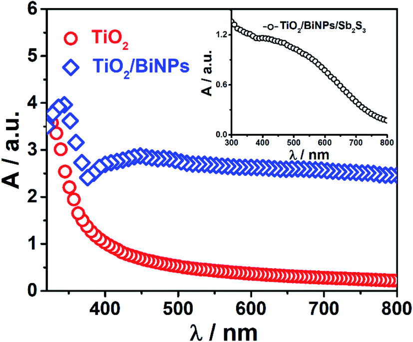 | ||
| Fig. 2 Absorption spectra of the TiO2 and TiO2/BiNP electrodes. Inset: absorption spectrum of the TiO2/BiNP/Sb2S3 electrode. | ||
To evaluate the plasmonic effect of BiNPs on the PEC activity of the ternary electrode, we examined the photocurrent response by each photoanode (TiO2 alone, TiO2/Sb2S3 or TiO2/BiNP/Sb2S3) by linearly sweeping the voltage (LSV plots) in a three-electrode system (Ag/AgCl as the reference electrode and Pt as the counter electrode), and the results are summarized in Fig. 3a. The pH of the electrolyte was set at 12.7 and the cells are illuminated with simulated sunlight (AM1.5). All the potentials reported against the reversible hydrogen electrode (RHE) are calculated using the Nernst equation. Upon chopped light illumination, the photocurrent density values for TiO2, TiO2/BiNP, TiO2/Sb2S3 and TiO2/BiNP/Sb2S3 photoanodes are 0.15, 0.61, 1.83 and 4.21 mA cm−2, respectively, at 1.23 V. The highest photo-response in terms of current density is observed for TiO2/BiNP/Sb2S3 at the lowest onset potential of 0.13 V. The enhanced photocurrent density of the TiO2/BiNP/Sb2S3 electrode, which is promising for PEC water splitting, is attributed to the ability of Sb2S3 to absorb the visible-NIR light and the SPR of BiNPs. In addition, the efficiency of a photoelectrode is expressed in terms of solar to hydrogen conversion (STH). The STH conversion efficiencies for TiO2, TiO2/BiNP, TiO2/Sb2S3 and TiO2/BiNP/Sb2S3 are estimated at 0.03, 0.22, 0.51 and 1.56% at 0.6 V (Fig. 3b), which are calculated from short circuit current density and the intensity of incident light (ESI†). The TiO2/BiNP/Sb2S3 photoanode provides us with 3- and 15-times higher STH conversion efficiency than TiO2/Sb2S3 and TiO2, respectively. Furthermore, estimation of the PEC water splitting performance of the TiO2/Sb2S3/BiNP electrode was carried out by using LSV plots and the results are presented in Fig. S6a.† Upon chopped light illumination, the TiO2/Sb2S3/BiNP electrode showed a maximum photocurrent density of 3.16 mA cm−2 at 1.23 V. Further, the high STH conversion efficiency of the TiO2/Sb2S3/BiNP electrode is 0.68% at 0.6 V (Fig. S6b†). Therefore, the TiO2/Sb2S3/BiNP electrode provides lower photocurrent density and STH efficiency than the TiO2/Bi/Sb2S3 electrode. These results suggested that BiNP-embedded TiO2/Sb2S3 can be better understood based on the staggered energy alignment of the TiO2/Bi/Sb2S3 compared to BiNPs grown on the surface of Sb2S3 (TiO2/Sb2S3/BiNP) for improving PEC water splitting.
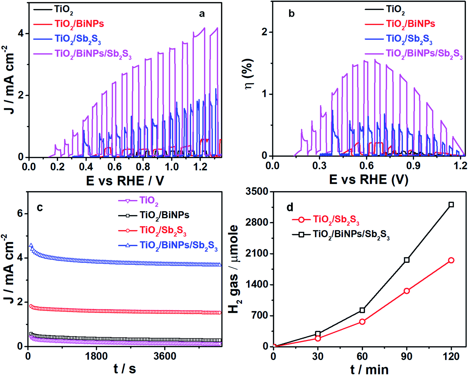 | ||
| Fig. 3 PEC properties of photoanodes. (a) LSV plots, (b) solar to hydrogen conversion efficiency and (c) photocurrent stability plots of TiO2, TiO2/BiNP, TiO2/Sb2S3 and TiO2/BiNP/Sb2S3 electrodes. Here 0.1 M Na2SO3 and 0.1 M Na2SO4 are used as the electrolyte solution under simulated solar irradiation. (d) Temporal evolution of H2 gas by TiO2/Sb2S3 and TiO2/BiNP/Sb2S3 electrodes. | ||
The stability of the photocurrent response by TiO2, TiO2/BiNP, TiO2/Sb2S3 and TiO2/BiNP/Sb2S3 photoanodes is examined by chronoamperometric (I–t curve) studies. Also, the photocurrent responses of the electrodes are tested at 1.23 V versus RHE (0.6 versus Ag/AgCl) under simulated solar (AM1.5) irradiation, and the results are presented in Fig. 3c. The long-term stability of the ternary electrode is noteworthy; only little decay in performance is observed after 5100 s. H2 evolution is quantified using gas chromatography and the amount of H2 evolved is plotted as a function of time at 1.23 V vs. RHE. As shown in Fig. 3d, the TiO2/BiNP/Sb2S3 photoanode provides maximum (3.2 mmol) H2 evolution over 2 h, which is when compared to TiO2/Sb2S3. The high photocurrent efficiency and H2 evolution performances of TiO2/BiNP/Sb2S3 are in good agreement.
The ability of photoelectrodes to convert the incident photons into electrons is examined by IPCE experiments in a two-electrode system, but without applying any external bias, as shown in Fig. 4a. The maximum IPCE for TiO2 is 13% in the UV region (300–400 nm), which is negligibly small in the visible to NIR region (400–900 nm). We find an increase in the IPCE for the TiO2 electrode supplemented with BiNPs, which is 15% in the UV region (300–400 nm) and additional contribution of 2–5% in the 400–800 nm region. This enhancement in IPCE performance by BiNPs is attributed to their SPR in the visible to NIR region. When compared to the 13% IPCE of TiO2 alone, the TiO2/Sb2S3 electrode shows ca. 20% IPCE in the 300–750 nm region, which is attributed to the small bandgap of Sb2S3. Thus, by combining the plasmonic effect of BiNPs with the small bandgap of Sb2S3 in TiO2/BiNP/Sb2S3, we accomplish 31% IPCE for the ternary photoanode. Also, this result implies that BiNPs in the heterojunction suppress undesired recombination of photogenerated charge carriers in Sb2S3.
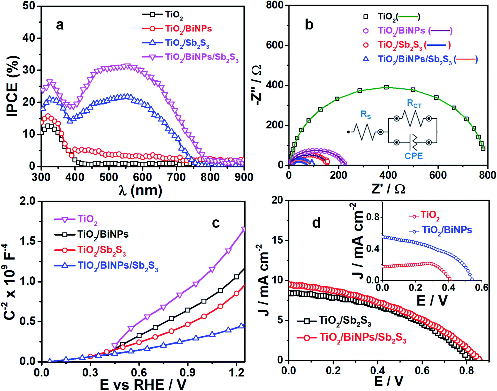 | ||
| Fig. 4 IPCE and I/V/R characteristics of photoanodes. (a) Wavelength-dependent IPCE plots (b) Nyquist plots (symbol) with an equivalent circuit (dot lines) and (c) Mott–Schottky plots of pristine TiO2, TiO2/BiNP, TiO2/Sb2S3 and TiO2/BiNP/Sb2S3 photoanodes. (d) J–V data of TiO2/Sb2S3 and TiO2/BiNP/Sb2S3 photoanodes. | ||
The kinetics of charge injection at the photoanode/electrolyte interfaces are studied by measuring the resistance across the electrode/electrolyte interface. Here impedance measurements were carried out under the light illumination of TiO2, TiO2/BiNP, TiO2/Sb2S3 or TiO2/BiNP/Sb2S3 electrodes immersed in a solution of 0.1 M Na2SO3 and 0.1 M Na2SO4 (1![[thin space (1/6-em)]](https://www.rsc.org/images/entities/char_2009.gif) :1, v/v) and the plots were fitted into the equivalent circuits shown in the inset in Fig. 4b, where RS, RCT and CPE represent the electrolyte solution resistance, interfacial charge transfer resistance at electrode/electrolyte and constant phase element for photoelectrode/electrolyte, respectively. The fitted parameters are given in Table 2 (ESI†). All the electrodes have solution resistance (RS) in the range of 4–9 Ω. The high RCT value of 775 Ω for TiO2 is due to low charge separation and the lowest RCT value of 71 Ω is observed for the TiO2/BiNP/Sb2S3 photoanode compared to other electrodes, indicating the facile transfer of charge carriers at the TiO2/BiNP/Sb2S3 photoanode/electrolyte interface, which is consistent with the excellent PEC performance of the electrode. Also, these charge injection properties are consistent with the electron lifetime (τ) values estimated from Bode plots (Fig. S7†). The τ values are estimated using the relation τ = 1/(2πƒmax) where ƒmax is the frequency maxima. The τ values calculated for pristine TiO2, TiO2/BiNP, TiO2/Sb2S3 and TiO2/BiNP/Sb2S3 films are 1.13, 1.22, 1.46 and 1.65 ms, respectively. The large τ value corresponds to a high rate of carrier transport or low rate of undesired carrier recombination in the TiO2/BiNP/Sb2S3 photoelectrode, which is attributed to the effect of BiNPs. In other studies, BiNPs increase the τ value of TiO2/BiNP/Sb2S3, which is in good agreement with the higher photocurrent density. Furthermore, we construct the Mott–Schottky plots of electrodes (Fig. 4c), where the linear profiles with positive slopes confirm the n-type characteristics of the photoanodes.
:1, v/v) and the plots were fitted into the equivalent circuits shown in the inset in Fig. 4b, where RS, RCT and CPE represent the electrolyte solution resistance, interfacial charge transfer resistance at electrode/electrolyte and constant phase element for photoelectrode/electrolyte, respectively. The fitted parameters are given in Table 2 (ESI†). All the electrodes have solution resistance (RS) in the range of 4–9 Ω. The high RCT value of 775 Ω for TiO2 is due to low charge separation and the lowest RCT value of 71 Ω is observed for the TiO2/BiNP/Sb2S3 photoanode compared to other electrodes, indicating the facile transfer of charge carriers at the TiO2/BiNP/Sb2S3 photoanode/electrolyte interface, which is consistent with the excellent PEC performance of the electrode. Also, these charge injection properties are consistent with the electron lifetime (τ) values estimated from Bode plots (Fig. S7†). The τ values are estimated using the relation τ = 1/(2πƒmax) where ƒmax is the frequency maxima. The τ values calculated for pristine TiO2, TiO2/BiNP, TiO2/Sb2S3 and TiO2/BiNP/Sb2S3 films are 1.13, 1.22, 1.46 and 1.65 ms, respectively. The large τ value corresponds to a high rate of carrier transport or low rate of undesired carrier recombination in the TiO2/BiNP/Sb2S3 photoelectrode, which is attributed to the effect of BiNPs. In other studies, BiNPs increase the τ value of TiO2/BiNP/Sb2S3, which is in good agreement with the higher photocurrent density. Furthermore, we construct the Mott–Schottky plots of electrodes (Fig. 4c), where the linear profiles with positive slopes confirm the n-type characteristics of the photoanodes.
To evaluate the role of plasmonic BiNPs on the power conversion efficiency of the ternary electrode, we constructed different photoelectrochemical solar cells and recorded the current–voltage (J–V) characteristics of the cells under 1 sun illumination (100 mW cm−2). Here the electrolyte used was polysulfide (0.1 M Na2S and 0.1 M S) solution. The active area of the working electrode (TiO2, TiO2/Sb2S3, or TiO2/BiNP/Sb2S3) was set at 0.15 cm2, and the counter electrode used was C-fabric. The J–V responses of the cells are shown in Fig. 4d and the solar cell parameters are summarized in Table S1 (ESI†). The TiO2/BiNP/Sb2S3 cell shows an open circuit voltage (VOC) of ∼860 mV and a short circuit current density (JSC) of 9.54 mA cm−2, which are greater than those of the TiO2/Sb2S3 electrode. The power conversion efficiency (PCE) of cells with TiO2, TiO2/Bi, TiO2/Sb2S3 and TiO2/BiNP/Sb2S3 electrodes is 0.019, 0.39, 2.99 and 3.85% respectively. The TiO2/BiNP/Sb2S3 based cells achieved the highest PCE and VOC was also the highest for this cell compared to the other electrodes. The high value of VOC is attributed to the bending of bands and improvement of charge separation induced by BiNPs. We attribute the high JSC value to the SPR effect of BiNPs, which increases the carrier density. These NPs not only transfer the photogenerated electrons from Sb2S3 to FTO via TiO2 but also act as photosensitizers, which are obvious from the high JSC and VOC values of FTO/TiO2/BiNP when compared with FTO/TiO2. The J–V characteristics FTO-based electrodes are shown in the inset in Fig. 4d. Furthermore, the higher PCE (0.39%) of the FTO/TiO2/BiNP electrode, which is when compared with FTO/TiO2 (0.01%), suggests that BiNPs transfer photogenerated electrons to the external circuit. In addition, the TiO2/Bi electrode shows high JSC (0.56 mA cm−2) and VOC (0.54 V) compared to the pure TiO2 film which is due to different regions of the solar spectrum being absorbed and converted to current.
The Fermi level of BiNPs, and conduction (CB) and valence band (VB) positions of TiO2 and Sb2S3 are obtained from cyclic voltammetry (Fig. S8†). The procedure for calculations of band positions in the energy level diagram is as shown in the ESI.† The mechanism of PEC performance of the ternary photoanode TiO2/BiNP/Sb2S3 is schematically presented in Fig. 5. Here the simulated solar illumination of the electrode leads to the generation of electron/hole pairs in the conduction (CB)/valence bands (VB) of Sb2S3. The photogenerated holes in the VB of Sb2S3 react with the sacrificial reagent (SO32−) and hydroxyl ion to produce SO42− and oxygen. On the other hand, BiNPs assist the transport of photogenerated electrons through the external circuit to the counter electrode (Pt) where protons are reduced to liberate hydrogen. In this hypothetical mechanism, the primary role of BiNPs is to expedite the transfer of electrons from the conduction band of Sb2S3 to that of TiO2 and finally to the back contact FTO.
 | ||
| Fig. 5 A scheme of a PEC cell constructed using the ternary photoanode TiO2/BiNP/Sb2S3, showing the band alignment, charge transport and redox reactions under the simulated solar irradiation. | ||
In summary, by combining the low bandgap Sb2S3 with the plasmonic BiNPs in the ternary TiO2/BiNP/Sb2S3 photoanode, we find that the efficiencies of photocurrent generation and photoelectrochemical hydrogen evolution increase by an order of magnitude when compared with the pristine TiO2 electrode. This ternary photoanode shows photocurrent density as high as 4.21 mA cm−2 at 1.23 V with a solar to hydrogen conversion efficiency of 1.56% at 0.6 V. BiNPs deliver the SPR effect to Sb2S3 and increase the rate of electron transport from Sb2S3 to TiO2, and as a result, the maximum of IPCE becomes 31% and the solar power conversion efficiency becomes 3.85%. By expediting the transfer of photogenerated electrons from Sb2S3 to the TiO2 electrode, BiNPs increase the open circuit voltage up to 860 mV. Also, with the plasmonic nearfield effect, the short circuit current reaches up to 9.54 mA cm−2. Overall, by combining the earth-abundant and cost-effective plasmonic BiNPs and the narrow bandgap Sb2S3 on the TiO2 electrode, we develop a stable, ternary photoanode and accomplish high efficiency photocurrent generation and hydrogen evolution.
Experimental
Materials and samples
Antimony chloride (SbCl3), sodium thiosulfate (Na2S2O3), bismuth nitrate pentahydrate [Bi(NO3)3·5H2O], dimethyl sulfoxide (DMSO), sodium sulfate (Na2SO4), elemental sulfur, methanol and acetone were obtained from Aldrich. Titanium tetrachloride (TiCl4), sodium borohydride (NaBH4), sodium sulfide (Na2S), sodium sulfite (Na2SO3) and tannic acid were obtained from Merck. TiO2 paste (18NR-T) used for electrode preparation was obtained from Dyesol. Deionized water (resistivity ∼ 18.2 Ω cm) was obtained from a Millipore Direct-Q3 UV system. Fluorine doped tin oxide (FTO) glass (sheet resistance ∼ 25 Ω cm−2) was obtained from Pilkington.Preparation of photoanodes
The TiO2/BiNP/Sb2S3 ternary photoanode was prepared by the doctor-blade technique. The photoanode was fabricated as follows: TiO2 paste was coated onto the pre-cleaned FTO substrates by the doctor-blade method, which was followed by annealing the TiO2 film at 500 °C for 30 min to provide a thin layer of TiO2 on FTO. Further, the TiO2 film was immersed in a hot (70 °C) solution (40 mM in isopropanol) of TiCl4 for 30 min. The film was rinsed with DI water and annealed at 500 °C for 30 min to provide the uniform TiO2 electrode. Further, BiNPs were grown onto the TiO2 electrode. In brief, Bi(NO3)3·5H2O was dissolved in DMSO and a solution containing a mixture of NaBH4 and tannic acid was slowly added, which brought about the reduction of Bi3+ to Bi0 and the obtained BiNPs were dispersed in water for further studies. Finally, the TiO2 film was vertically introduced into the bismuth precursor solution and sonicated for 15 min to form the TiO2/BiNP film, which was brown in color. Further, Sb2S3 was grown onto the TiO2/BiNP film by the chemical bath deposition process to form the ternary electrode TiO2/BiNP/Sb2S3.47,48 Briefly, 400 mg of SbCl3 was dissolved in 2.5 mL of acetone, which was followed by the addition of 72.5 mL of deionized water to yield a turbid solution that subsequently converted into a white precipitate. Subsequently, 3.95 g of Na2S2O3 dissolved in 25 mL of water was added to the SbCl3 solution under stirring. The TiO2/BiNP film was vertically dipped in the Sb2S3 solution at 25 °C for 60 min, which was followed by rinsing the electrode with deionized water and drying on a hot plate at 60 °C. Finally, the film was annealed at 300 °C for 15 min under an argon atmosphere to yield the dark-orange colored TiO2/BiNP/Sb2S3 photoanode. Preparation of the electrode is illustrated in the ESI.†Characterization techniques
The surface morphologies of the samples were analyzed using a field emission scanning electron microscope (FESEM-Zeiss supra 40). High-resolution transmission electron microscope (HR-TEM) images were recorded using a TECNAI G-2 FEI instrument operating at 300 kV. The powder X-ray diffraction (XRD) patterns of samples were measured on a PANalytical, Xpert PRO instrument. The Raman spectra of photoanode materials were recorded by using a Bruker Senterra dispersive Raman microscope spectrometer with an excitation wavelength of 532 nm. The absorption spectra of the synthesized electrodes were recorded on a UV-Vis spectrophotometer (Shimadzu UV-3600). PEC measurements were performed in an aqueous electrolyte containing a 1:1 mixture of 0.1 M Na2SO3 and 0.1 M Na2SO4, using a three electrode system with Pt and Ag/AgCl as the counter and reference electrodes, respectively. The current versus potential (I–V) characteristics of photoanodes were recorded using a LOT-Oriel-Autolab with a 150 W xenon arc lamp with 100 mW cm−2 intensity. Chronoamperometric (I–t) plots, Mott–Schottky plots, cyclic voltammetry (CV) and electrochemical impedance spectra (EIS) were measured on an Autolab PGSTAT 302N equipped with NOVA 1.9 software. The irradiance intensity was confirmed by calibrating with a 2 cm × 2 cm Si Reference Cell and re-affirmed with a radiant power meter from Newport (842-PE). The IPCE was measured using a quantum efficiency measurement system (Oriel IQE-200), where 250 W quartz tungsten and halogen lamps were used as the light sources, the monochromator path length was 1/8M and the spot size was 1 mm × 2.5 mm rectangular at focus. This instrument gave the IPCE values as a function of wavelength directly.
Conflicts of interest
There are no conflicts to declare.Acknowledgements
PS thanks CSIR-HRDG, New Delhi for providing fellowship. CS, SSKR and VB acknowledge the financial support under the SPARC program of the Science and Engineering Research Board of India. VB acknowledges financial support under the MEXT JSPS Grant-in-Aid for Scientific Research B (19H02550). HM and VB acknowledge financial support under the MEXT JSPS Special Advancement Research Grant (18H05205).References
- M. G. Walter, E. L. Warren, J. R. McKone, S. W. Boettcher, Q. Mi, E. A. Santori and N. S. Lewis, Solar water splitting cells, Chem. Rev., 2010, 110, 6446–6473 CrossRef CAS.
- Y. Tachibana, L. Vayssieres and J. R. Durrant, Artificial photosynthesis for solar water-splitting, Nat. Photonics, 2012, 6, 511 CrossRef CAS.
- S. Y. Tee, K. Y. Win, W. S. Teo, L. D. Koh, S. Liu, C. P. Teng and M. Y. Han, Recent progress in energy-driven water splitting, Adv. Sci., 2017, 4, 1600337 CrossRef.
- S. C. Warren, K. Voïtchovsky, H. Dotan, C. M. Leroy, M. Cornuz, F. Stellacci, C. Hébert, A. Rothschild and M. Grätzel, Identifying champion nanostructures for solar water-splitting, Nat. Mater., 2013, 12, 842 CrossRef CAS.
- M. Grätzel, Photoelectrochemical cells, Nature, 2001, 414, 338 CrossRef.
- E. L. Miller, Photoelectrochemical water splitting, Energy Environ. Sci., 2015, 8, 2809–2810 RSC.
- K. Sivula and R. Van De Krol, Semiconducting materials for photoelectrochemical energy conversion, Nat. Rev. Mater., 2016, 1, 15010 CrossRef CAS.
- A. Fujishima and K. Honda, Electrochemical photolysis of water at a semiconductor electrode, Nature, 1972, 238, 37 CrossRef CAS.
- G. Wang, H. Wang, Y. Ling, Y. Tang, X. Yang, R. C. Fitzmorris, C. Wang, J. Z. Zhang and Y. Li, Hydrogen-treated TiO2 nanowire arrays for photoelectrochemical water splitting, Nano Lett., 2011, 11, 3026–3033 CrossRef CAS.
- I. S. Cho, Z. Chen, A. J. Forman, D. R. Kim, P. M. Rao, T. F. Jaramillo and X. Zheng, Branched TiO2 nanorods for photoelectrochemical hydrogen production, Nano Lett., 2011, 11, 4978–4984 CrossRef CAS.
- S. Liang, J. He, Z. Sun, Q. Liu, Y. Jiang, H. Cheng, B. He, Z. Xie and S. Wei, Improving photoelectrochemical water splitting activity of TiO2 nanotube arrays by tuning geometrical parameters, J. Phys. Chem. C, 2012, 116, 9049–9053 CrossRef CAS.
- P. Pathak, S. Gupta, K. Grosulak, H. Imahori and V. Subramanian, Nature-inspired tree-like TiO2 architecture: a 3D platform for the assembly of CdS and reduced graphene oxide for photoelectrochemical processes, J. Phys. Chem. C, 2015, 119, 7543–7553 CrossRef CAS.
- P. Subramanyam, P. N. Kumar, M. Deepa, C. Subrahmanyam and P. Ghosal, Bismuth sulfide nanocrystals and gold nanorods increase the photovoltaic response of a TiO2/CdS based cell, Sol. Energy Mater. Sol. Cells, 2017, 159, 296–306 CrossRef CAS.
- X. Wang, J. Xie and C. M. Li, Architecting smart “umbrella” Bi2S3/rGO-modified TiO2 nanorod array structures at the nanoscale for efficient photoelectrocatalysis under visible light, J. Mater. Chem. A, 2015, 3, 1235–1242 RSC.
- P. Subramanyam, T. Vinodkumar, M. Deepa and C. Subrahmanyam, Gold nanoparticle decorated bismuth sulfide nanorods for enhanced photoelectrochemical hydrogen production, J. Mater. Chem. C, 2019, 7, 6398–6405 RSC.
- D. V. Freitas, J. R. González-Moya, T. A. Soares, R. R. Silva, D. M. Oliveira, H. S. Mansur, G. Machado and M. Navarro, Enhanced visible-light photoelectrochemical conversion on TiO2 nanotubes with Bi2S3 quantum dots obtained by in situ electrochemical method, ACS Appl. Energy Mater., 2018, 1, 3636–3645 CrossRef CAS.
- S. Ho-Kimura, S. J. Moniz, A. D. Handoko and J. Tang, Enhanced photoelectrochemical water splitting by nanostructured BiVO4–TiO2 composite electrodes, J. Mater. Chem. A, 2014, 2, 3948–3953 RSC.
- H. Zhang and C. Cheng, Three-dimensional FTO/TiO2/BiVO4 composite inverse opals photoanode with excellent photoelectrochemical performance, ACS Energy Lett., 2017, 2, 813–821 CrossRef CAS.
- C. Liu, Y. Yang, W. Li, J. Li, Y. Li and Q. Chen, A novel Bi2S3 nanowire@TiO2 nanorod heterogeneous nanostructure for photoelectrochemical hydrogen generation, Chem. Eng. J., 2016, 302, 717–724 CrossRef CAS.
- J. Zhong, X. Zhang, Y. Zheng, M. Zheng, M. Wen, S. Wu, J. Gao, X. Gao, J. M. Liu and H. Zhao, High efficiency solar cells as fabricated by Sb2S3-modified TiO2 nanofibrous networks, ACS Appl. Mater. Interfaces, 2013, 5, 8345–8350 CrossRef CAS.
- H. Du, C. Yang, W. Pu, H. Zhao and J. Gong, Highly active Sb2S3 attached Mo–WO3 composite film for enhanced photoelectrocatalytic water splitting at extremely low input light energy, ACS Sustainable Chem. Eng., 2019, 7, 9172–9181 CrossRef CAS.
- A. D. DeAngelis, K. C. Kemp, N. Gaillard and K. S. Kim, Antimony(III) sulfide thin films as a photoanode material in photocatalytic water splitting, ACS Appl. Mater. Interfaces, 2016, 8, 8445–8451 CrossRef CAS.
- Z. Yang, X. Wang, Y. Chen, Z. Zheng, Z. Chen, W. Xu, W. Liu, Y. M. Yang, J. Zhao, T. Chen and H. Zhu, Ultrafast self-trapping of photoexcited carriers sets the upper limit on antimony trisulfide photovoltaic devices, Nat. Commun., 2019, 10, 1–8 CrossRef.
- Y. Wu, L. Assaud, C. Kryschi, B. Capon, C. Detavernier, L. Santinacci and J. Bachmann, Antimony sulfide as a light absorber in highly ordered, coaxial nanocylindrical arrays: preparation and integration into a photovoltaic device, J. Mater. Chem. A, 2015, 3, 5971–5981 RSC.
- Y. Itzhaik, O. Niitsoo, M. Page and G. Hodes, Sb2S3-sensitized nanoporous TiO2 solar cells, J. Phys. Chem. C, 2009, 113, 4254–4256 CrossRef CAS.
- J. Zhang, Z. Liu and Z. Liu, Novel WO3/Sb2S3 heterojunction photocatalyst based on WO3 of different morphologies for enhanced efficiency in photoelectrochemical water splitting, ACS Appl. Mater. Interfaces, 2016, 8, 9684–9691 CrossRef CAS.
- Y. T. Song, L. Y. Lin, Y. S. Chen, H. Q. Chen, Z. D. Ni, C. C. Tu and S. S. Yang, Novel TiO2/Sb2S3 heterojunction with whole visible-light response for photoelectrochemical water splitting reactions, RSC Adv., 2016, 6, 49130–49137 RSC.
- Y. C. Pu, G. Wang, K. D. Chang, Y. Ling, Y. K. Lin, B. C. Fitzmorris, C. M. Liu, X. Lu, Y. Tong, J. Z. Zhang and Y. J. Hsu, Au nanostructure-decorated TiO2 nanowires exhibiting photoactivity across entire UV-visible region for photoelectrochemical water splitting, Nano Lett., 2013, 13, 3817–3823 CrossRef CAS.
- H. J. Kim, S. H. Lee, A. A. Upadhye, I. Ro, M. I. Tejedor-Tejedor, M. A. Anderson, W. B. Kim and G. W. Huber, Plasmon-enhanced photoelectrochemical water splitting with size-controllable gold nanodot arrays, ACS Nano, 2014, 8, 10756–10765 CrossRef CAS.
- X. Shi, K. Ueno, T. Oshikiri, Q. Sun, K. Sasaki and H. Misawa, Enhanced water splitting under modal strong coupling conditions, Nat. Nanotechnol., 2018, 13, 953–958 CrossRef CAS.
- H. Li, Z. Li, Y. Yu, Y. Ma, W. Yang, F. Wang, X. Yin and X. Wang, Surface-plasmon-resonance-enhanced photoelectrochemical water splitting from Au-nanoparticle-decorated 3D TiO2 nanorod architectures, J. Phys. Chem. C, 2017, 121, 12071–12079 CrossRef CAS.
- K. Qian, B. C. Sweeny, A. C. Johnston-Peck, W. Niu, J. O. Graham, J. S. DuChene, J. Qiu, Y. C. Wang, M. H. Engelhard, D. Su and E. A. Stach, Surface plasmon-driven water reduction: gold nanoparticle size matters, J. Am. Chem. Soc., 2014, 136, 9842–9845 CrossRef CAS.
- C. Peng, W. Wang, W. Zhang, Y. Liang and L. Zhuo, Surface plasmon-driven photoelectrochemical water splitting of TiO2 nanowires decorated with Ag nanoparticles under visible light illumination, Appl. Surf. Sci., 2017, 420, 286–295 CrossRef CAS.
- Q. Wang, J. Qiao, X. Xu and S. Gao, Controlled synthesis of Cu nanoparticles on TiO2 nanotube array photoelectrodes and their photoelectrochemical properties, Mater. Lett., 2014, 131, 135–137 CrossRef CAS.
- S. Linic, P. Christopher and D. B. Ingram, Plasmonic-metal nanostructures for efficient conversion of solar to chemical energy, Nat. Mater., 2011, 10, 911 CrossRef CAS.
- J. Li, S. K. Cushing, F. Meng, T. R. Senty, A. D. Bristow and N. Wu, Plasmon-induced resonance energy transfer for solar energy conversion, Nat. Photonics, 2015, 9, 601 CrossRef CAS.
- P. V. Kamat and G. V. Hartland, Plasmons for Energy Conversion, ACS Energy Lett., 2018, 3, 1467–1469 CrossRef CAS.
- S. C. Warren and E. Thimsen, Plasmonic solar water splitting, Energy Environ. Sci., 2012, 5, 5133–5146 RSC.
- X. Yang, H. Li, W. Zhang, M. Sun, L. Li, N. Xu, J. Wu and J. Sun, High visible photoelectrochemical activity of Ag nanoparticle-sandwiched CdS/Ag/ZnO nanorods, ACS Appl. Mater. Interfaces, 2017, 9, 658–667 CrossRef CAS.
- J. Li, S. K. Cushing, P. Zheng, T. Senty, F. Meng, A. D. Bristow, A. Manivannan and N. Wu, Solar hydrogen generation by a CdS–Au–TiO2 sandwich nanorod array enhanced with Au nanoparticle as electron relay and plasmonic photosensitizer, J. Am. Chem. Soc., 2014, 136, 8438–8449 CrossRef CAS.
- J. Toudert, R. Serna and M. Jimenez de Castro, Exploring the optical potential of nano-bismuth: tunable surface plasmon resonances in the near ultraviolet-to-near infrared range, J. Phys. Chem. C, 2012, 116, 20530–20539 CrossRef CAS.
- F. Dong, T. Xiong, Y. Sun, Z. Zhao, Y. Zhou, X. Feng and Z. Wu, A semimetal bismuth element as a direct plasmonic photocatalyst, Chem. Commun., 2014, 50, 10386–10389 RSC.
- W. Fan, C. Li, H. Bai, Y. Zhao, B. Luo, Y. Li, Y. Ge, W. Shi and H. Li, An in situ photoelectroreduction approach to fabricate Bi/BiOCl heterostructure photocathodes: understanding the role of Bi metal for solar water splitting, J. Mater. Chem. A, 2017, 5, 4894–4903 RSC.
- J. Wang, L. Tang, G. Zeng, Y. Liu, Y. Zhou, Y. Deng, J. Wang and B. Peng, Plasmonic Bi metal deposition and g-C3N4 coating on Bi2WO6 microspheres for efficient visible-light photocatalysis, ACS Sustainable Chem. Eng., 2016, 5, 1062–1072 CrossRef.
- Z. Zhao, W. Zhang, Y. Sun, J. Yu, Y. Zhang, H. Wang, F. Dong and Z. Wu, Bi cocatalyst/Bi2MoO6 microspheres nanohybrid with SPR-promoted visible-light photocatalysis, J. Phys. Chem. C, 2016, 120, 11889–11898 CrossRef CAS.
- B. R. Wulan, S. S. Yi, S. J. Li, Y. X. Duan, J. M. Yan, X. B. Zhang and Q. Jiang, Non-noble-metal bismuth nanoparticle-decorated bismuth vanadate nanoarray photoanode for efficient water splitting, Mater. Chem. Front., 2018, 2, 1799–1804 RSC.
- Y. Li, L. Wei, R. Zhang, Y. Chen, L. Mei and J. Jiao, Annealing effect on Sb2S3–TiO2 nanostructures for solar cell applications, Nanoscale Res. Lett., 2013, 8, 89 CrossRef.
- D. U. Lee, S. Woo Pak, S. Gook Cho, E. Kyu Kim and S. Il Seok, Defect states in hybrid solar cells consisting of Sb2S3 quantum dots and TiO2 nanoparticles, Appl. Phys. Lett., 2013, 103, 023901 CrossRef.
- Z. Zhao, W. Zhang, X. Lv, Y. Sun, F. Dong and Y. Zhang, Noble metal-free Bi nanoparticles supported on TiO2 with plasmon-enhanced visible light photocatalytic air purification, Environ. Sci.: Nano, 2016, 3, 1306–1317 RSC.
- Y. Chen, D. Chen, J. Chen, Q. Lu, M. Zhang, B. Liu, Q. Wang and Z. Wang, Facile synthesis of Bi nanoparticle modified TiO2 with enhanced visible light photocatalytic activity, J. Alloys Compd., 2015, 651, 114–120 CrossRef CAS.
Footnote |
| † Electronic supplementary information (ESI) available. See DOI: 10.1039/d0na00641f |
| This journal is © The Royal Society of Chemistry 2020 |