
Microsecond charge separation at heterojunctions between transition metal dichalcogenide monolayers and single-walled carbon nanotubes†
Dana B.
Sulas-Kern
 ,
Hanyu
Zhang
,
Zhaodong
Li
and
Jeffrey L.
Blackburn
*
,
Hanyu
Zhang
,
Zhaodong
Li
and
Jeffrey L.
Blackburn
*
National Renewable Energy Laboratory, Golden, Colorado 80401, USA. E-mail: Jeffrey.blackburn@nrel.gov
First published on 12th July 2019
Abstract
The use of monolayer transition metal dichalcogenides (TMDCs) for optical-to-electrical or optical-to-chemical energy conversion can be limited by the ultrafast excited state relaxation inherent to neat monolayers. Photoinduced charge separation at nanoscale heterojunctions is an important strategy to extend carrier lifetimes, enabling photodetectors, solar cells, and solar fuel production with these ultrathin materials. We demonstrate TMDC/single-walled carbon nanotube (SWCNT) heterojunctions with exceptionally long, microsecond timescale, charge separation following sub-picosecond interfacial charge transfer. These carrier lifetimes are orders of magnitude longer-lived than in other monolayer TMDC heterojunctions. We further present two unique methodologies for estimating charge-transfer quantum yields in MoS2 that can be broadly applied and refined for other TMDC systems. Our results highlight the promise of TMDC/SWCNT heterojunctions for advanced (photo)catalytic and optoelectronic systems and devices.
New conceptsLong-lived separated charge carriers are a prerequisite for efficiently converting photon energy to electricity or fuels in solar energy harvesting devices. Here, we counteract ultrafast excited state decay in transition metal dichalcogenide (TMDC) monolayers by demonstrating that heterojunctions between MoS2 and single-walled carbon nanotubes enable remarkably long carrier lifetimes in the microsecond time range. The photoexcited free charges in this system differ from the Coulomb-bound interfacial states found in several other TMDC heterojunctions, and the long lifetimes in this case may enable facile current extraction and complex multi-electron photocatalytic reactions, opening avenues for efficient photocurrent generation and hydrogen evolution. With a goal of enabling systematic investigations of charge separation in TMDCs and their heterojunctions, we introduce broadly applicable concepts for quantifying practical metrics necessary for high-efficiency devices (e.g. carrier lifetimes, yields, and generation rates) and for analysing the fundamental mechanisms underlying charge separation. |
Introduction
Two-dimensional (2D) transition metal dichalcogenides (TMDCs) have received recent attention for their promise in catalytic,1–3 logic,6 semiconducting,7–9 and optoelectronic devices.10–13 Although initial discovery of TMDCs dates back to 192315 and monolayers were achieved in 1986,16 the advances necessary to harness the exceptional properties of TMDC monolayers came much later with graphene-related development in the early 2000's,17 spurring a rapid increase in TMDC interest over the past five years.18,19 Unlike graphene, many TMDCs have a natural band gap in the visible range, enabling light-harvesting applications with a similarly ultrathin material. The synergy between confined spatial structure and the unique TMDC energy landscape (for example, including a spin–orbit split valence band and a transition from indirect to direct band gap at the monolayer limit20,21) introduces a vast array of technologically valuable phenomena such as chemical and mechanical tunability of the band structure and excited state populations,22–25 spin-valley locking,26,27 quantum confinement,21,28,29 high absorption coefficients,10 excellent thickness-normalized device metrics,10,12 large magnetoresistance,30,31 and superconductivity.18,31,32Despite the great promise and rich (photo)physics in TMDCs, the performance of TMDC devices that rely on efficient photocurrent generation can be limited by large exciton binding energies5,33,34 and the resulting ultrafast excited state decay that is often observed on picosecond time scales.35 For example, while TMDCs such as MoS2 show promise as stable, earth-abundant, and cost-effective (photo)catalysts for hydrogen fuel production, high photocatalytic activity depends upon achieving sufficiently long carrier lifetimes for electron diffusion to active sites and subsequent transfer from the TMDC to adsorbed hydrogen.3 Similarly, in photovoltaic applications, fast recombination in competition with charge extraction is likely an important factor causing sub-unity internal quantum efficiencies and low open-circuit voltages.12,13 To realize the long carrier lifetimes necessary for functional TMDC applications, several hybrid structures are actively being investigated (e.g. stacked TMDC/TMDC,13,36,37 lateral multilayer–monolayer TMDC,38–40 TMDC/graphene,6 TMDC/organic,12,41–44 TMDC/quantum dots,45 TMDC/Si,46 TMDC/carbon nitride47), where charge transfer across a heterojunction combats recombination and extends excited state lifetimes through exciton dissociation and spatial separation of electrons from holes.
While charge carrier lifetimes have been extended up to nanosecond time scales in some of these TMDC heterojunctions,42,44 in this study we demonstrate orders of magnitude longer-lived kinetics with carriers persisting past 1 μs in Type-II heterojunctions of monolayer MoS2 with (6,5) semiconducting single-walled carbon nanotube (SWCNT) films. The pairing of MoS2 with SWCNTs is particularly appealing due to the diameter-dependent tunability of the SWCNT energy landscape,48 the high photochemical stability of SWCNTs,49 and previous demonstrations of SWCNTs sustaining long-lived charge in other donor/acceptor heterojunctions.14,50,51 Encouragingly, both photocurrent and hydrogen evolution have been observed in a few TMDC/SWCNT systems, although these systems most often contain mixed SWCNTs with a broad range of electronic structure and amorphous or multilayer TMDCs.2,49,52,53
Because the fundamental photophysical processes at monolayer TMDC/SWCNT heterojunctions have been largely unexplored, we present a detailed model of the ultrafast charge-transfer process leading to exceptionally long-lived separated charges. By fitting our transient absorption (TA) data using a global target analysis based on singular value decomposition,54 we quantify sub-picosecond charge generation, including both electron transfer to MoS2 following selective SWCNT excitation (τET ≈ 0.8 ps) and hole transfer to the SWCNT layer following selective MoS2 excitation (τHT ≈ 0.5 ps). We evaluate charge-transfer yields based on the empirically-determined SWCNT absorption cross section,50 and we further discuss the charge-transfer yields in the context of a phase-space filling model that relates the magnitude of MoS2 carrier-induced exciton quenching to the MoS2 dielectric constant and exciton mass. Our study highlights the promise of pairing SWCNTs with TMDC monolayers both for sustaining remarkably long-lived charge carriers in photocatalytic and optoelectronic applications and for use as clean model systems with easily distinguishable and quantifiable spectral signatures for optical studies.
Experimental results
MoS2/SWCNT heterojunctions
Fig. 1A depicts the energy level offsets at the monolayer MoS2/(6,5)SWCNT interface, showing that this system is expected to form a Type-II heterojunction. In Fig. 1B, we illustrate that charge transfer generates negative charge on MoS2 after photoexcitation of either layer (process 1), after which efficient charge transport and delocalization within the SWCNT layer55,56 likely serves an essential role to prevent recombination at the interface by supporting spatial carrier separation (process 2). As our schematic implies, the ultrathin nature of MoS2 monolayers limit the vertical distance that electrons can move away from the interface, suggesting that hole transport in the SWCNT layer may be crucial for sustaining long-lived charge.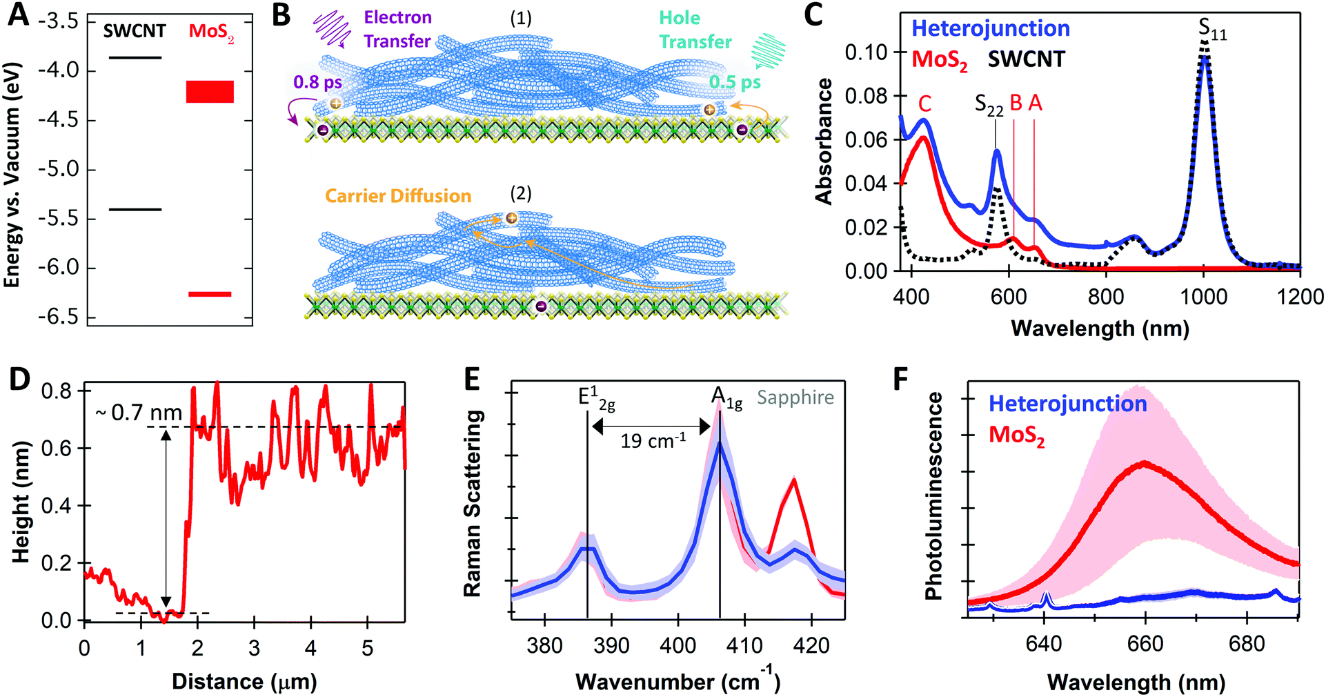 | ||
| Fig. 1 (A) Energy level diagram for monolayer MoS2 and (6,5)SWCNTs with values from ref. 5 and 14; (B) schematic of (1) photoexcited charge transfer and (2) carrier diffusion, with time constants from our transient absorption analysis; (C) absorbance spectra for neat MoS2 (red), neat SWCNT (black dotted), and MoS2/SWCNT heterojunctions (blue); (D) atomic force microscopy height profile across a scratch for the neat MoS2 monolayer; (E) Raman scattering for neat MoS2 (red) and the heterojunction (blue); (F) photoluminescence spectra for MoS2 (red) and MoS2/SWCNT heterojunctions (blue), where sharp peaks in the heterojunction spectrum are SWCNT Raman modes. Shading in (E and F) represents the standard deviation of the mean for 15 measurements with 532 nm excitation, which likely arises from variations in local chemical environment and substrate interactions. | ||
The thermodynamic driving force for free carrier generation depends on the energetic difference between initially photoexcited excitons and the final separated charges. We estimate the driving force as ΔGET/HT = (IPD − EAA) − Eopt,D/opt,A, where ΔGET/HT is the change in free energy following electron transfer (ET) or hole transfer (HT), IPD and Eopt,D are the ionization potential and optical gap of the SWCNT donor, and EAA and Eopt,A are the electron affinity and optical gap of the MoS2 acceptor.57 Using the energies in Fig. 1A, we estimate that MoS2 exciton dissociation followed by hole transfer to the SWCNTs is favorable by −620 meV. Calculating ΔGET has more significant uncertainty due to greater variation of the MoS2 electron affinity in the literature. Using reported values of EAMoS2 of −4.15 to −4.25 eV,5 we estimate ΔGET in the range of −90 to +10 meV. We note that MoS2 excitation can also result in excitation energy transfer (EET) from MoS2 to SWCNTs due to the larger bandgap of MoS2.
As shown in Fig. 1C, the complementary absorbance peaks of MoS2 and (6,5)SWCNTs make this an ideal model system for optical studies of excited-state dynamics at TMDC heterojunctions. The S11 absorption at 1000 nm allows selective photoexcitation of low-energy SWCNT excitons. Subsequently, charge transfer is the only pathway for moving a carrier population onto MoS2, because the 1000 nm photons are too low in energy for direct MoS2 excitation and EET from SWCNTs to MoS2 is significantly uphill in energy. Additionally, the MoS2 C exciton absorption at 440 nm peaks at an absorption minimum for the SWCNTs, allowing selective probing of hole transfer from MoS2 to the SWCNTs. Furthermore, the MoS2 A (660 nm) and B (610 nm) exciton peaks show minimal overlap with the SWCNT S22 absorption, allowing us to clearly track MoS2 bleaching during TA analysis. This clean spectral separation contrasts with previous heterojunction studies where overlapping absorption spectra must be carefully considered to evaluate charge separation mechanisms from optical studies.42,44
Fig. 1D–F demonstrate that the MoS2 used in our studies are indeed monolayers. The ∼0.7 nm atomic force microscopy (AFM) height profile (Fig. 1D), the 19 cm−1 energy difference between in-plane (E12g) and out-of-plane (A1g) Raman peaks (Fig. 1E), and the 660 nm photoluminescence (PL) peak position (Fig. 1F) are all characteristic of monolayers.25,58
Long-lived photoinduced charge formation
In Fig. 1F, the MoS2 PL is strongly quenched in the MoS2/SWCNT heterojunction compared to the neat monolayer, suggesting that photoinduced charge transfer likely occurs across the heterojunction. However, PL quenching cannot discern between charge and energy transfer, as both processes deplete emissive MoS2 excitons. Thus, we use transient absorption (TA) spectroscopy to quantify charge transfer at MoS2/SWCNT interfaces. We show that separated carriers form with sub-picosecond kinetics following selective photoexcitation of either the MoS2 or the SWCNT layers and that charge separation persists up to the microsecond timescale.Fig. 2A and C show the long-lived TA spectra that persist in the heterojunction following both 440 and 1000 nm excitation. With either excitation wavelength, the NIR signal in the heterojunction is enhanced compared to the neat materials. The NIR peaks are signatures of a SWCNT charge carrier population, including the trion induced absorption at 1175 nm and bleaching of the S11 transition at 1000 nm.50 The SWCNT charge signatures in the heterojunction indicate that both processes are thermodynamically and kinetically accessible, including photoinduced hole transfer from excited MoS2 to the SWCNT layer (Fig. 2A, 440 nm excitation) and electron transfer from SWCNTs to MoS2 (Fig. 2C, 1000 nm excitation).
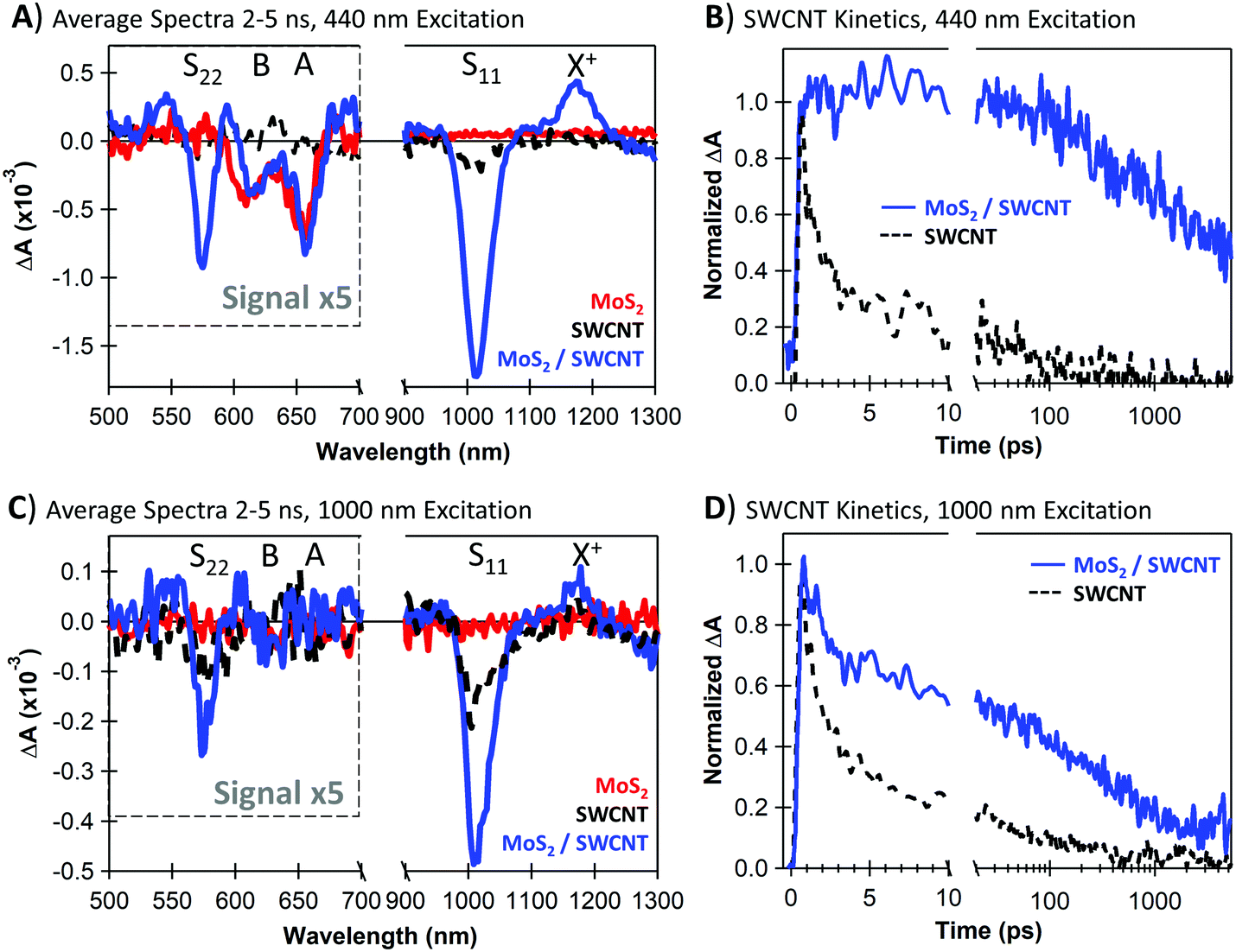 | ||
| Fig. 2 (A) Transient absorption spectra averaged over 2–5 ns following 440 nm excitation of neat MoS2 (red), neat SWCNT (black dotted), and MoS2/SWCNT heterojunctions (blue); (B) kinetic traces at 1175 nm, corresponding to the SWCNT trion (X+) induced absorption with 440 nm excitation; (C) transient absorption spectra averaged over 2–5 ns following 1000 nm excitation; (D) kinetic traces at the SWCNT trion induced absorption with 1000 nm excitation. | ||
In the visible range, we attribute bleaching at 610 nm and 650 nm to the MoS2 A and B excitons, respectively, and we attribute the 575 nm bleach to the SWCNT S22 transition. We observe MoS2 bleaching even with low-energy 1000 nm excitation, indicating that electron transfer from the SWCNTs to MoS2 must take place. The 440 nm excitation generates similar MoS2 bleach magnitude in both the heterojunction and neat monolayer. We note that the unchanged MoS2 bleach amplitude in this case does suggest that a greater electron density is sustained on MoS2 with the heterojunction. This is because the bleach in neat MoS2 is either due to excitons or a mix of spontaneously separated electrons and holes, while the bleach in the heterojunction is primarily due to only electrons after the holes are donated to the SWCNTs. The demonstration of both photoinduced hole transfer from MoS2 to SWCNT and electron transfer from SWCNT to MoS2 is consistent with the Type-II energetic alignment and thermodynamic driving forces proposed in Fig. 1A.
In Fig. 2B and D, we show the charge-related kinetics at the SWCNT trion induced absorption at 1175 nm, demonstrating longer-lived carrier kinetics in the heterojunctions compared to the neat SWCNTs. Importantly, the charge-associated signal in the heterojunction does not fully decay within the 5 ns delay window regardless of the excitation wavelength. We note that the heterojunction kinetics with 1000 nm excitation in Fig. 2D show an initial fast decay component corresponding to SWCNT excitons that have non-negligible contribution to the signal at 1175 nm (further discussed in Fig. 4A). The SWCNT excitons either decay to the ground state or undergo charge separation, and longer-lived carrier kinetics similar to the 440 nm excitation dominate at later times.
Fig. 3 shows that the separated charge carriers persist up to the microsecond time scale in the monolayer MoS2/SWCNT heterojunction, and that the kinetics on these longer time scales are similar for selective excitation of either MoS2 or the SWCNT layer. Recombination on long timescales follows a multiexponential decay with an amplitude-averaged lifetime of 0.73 μs from components of 17.5 ns (43%), 233 ns (43%), and 4.4 μs (14%). These kinetics demonstrate the longest carrier lifetimes to our knowledge in monolayer TMDC heterojunctions that have been measured with TA spectroscopy at room temperature.
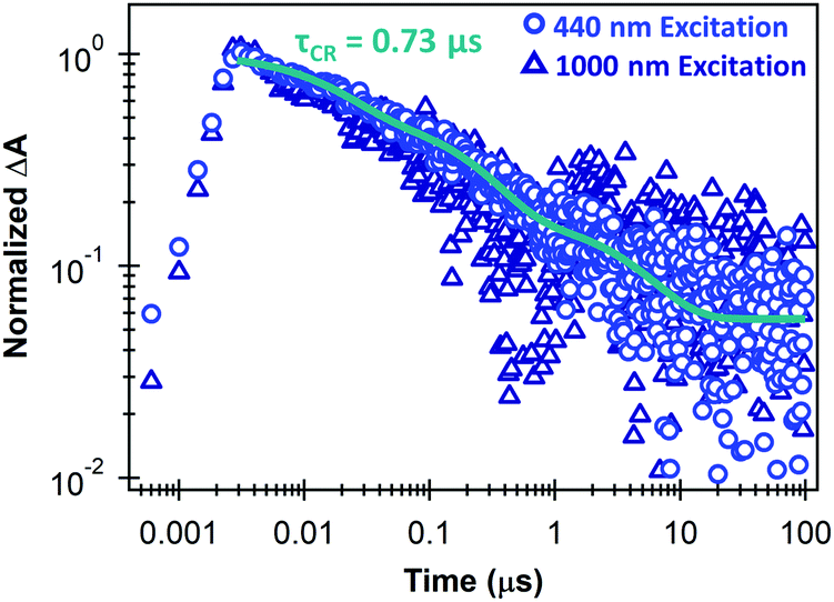 | ||
| Fig. 3 Carrier kinetics at 1175 nm (trion induced absorption) on the microsecond time scale for monolayer MoS2/SWCNT heterojunctions under 440 nm excitation (light blue circles) or 1000 nm excitation (dark blue triangles), showing a triexponential fit with an amplitude-averaged charge recombination time constant (τCR) of 0.73 μs. | ||
Global analysis to obtain charge transfer time constants
Although the large energetic separation between SWCNT and MoS2 spectral features allows us to easily track the recombination lifetimes of separated charges, it is non-trivial to extract accurate rise times for ultrafast charge separation due to the overlapping spectra of excitons and charges at early times. To quantify charge transfer kinetics, we separate the time-dependent spectral contributions of excitons and charges using a global analysis based on singular value decomposition (SVD).54 We discuss our fitting using TA data for hole transfer following 440 nm excitation (Fig. 4), and we provide fitting results for the neat materials as well as the heterojunction with 1000 nm excitation in the ESI.†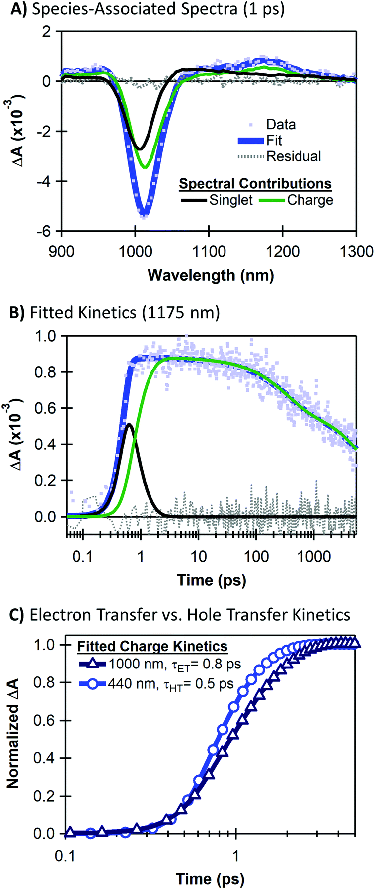 | ||
| Fig. 4 Example of NIR fitting results for the monolayer MoS2/SWCNT heterojunction with 440 nm pump including (A) the transient absorption spectrum at 1 ps (light blue points) overlaid with the singlet-associated (black trace) and charge-associated (green trace) spectral components, which are summed to create the total fit (blue trace) giving minimal residual fitting error (gray dotted trace); (B) kinetics at 1175 nm (light blue points) overlaid with the time-dependent profiles corresponding to the spectral components in (A) which are summed to create the total fit (blue trace) giving minimal residual error (gray dotted trace); (C) comparison of the charge-associated kinetics fits showing faster rise for the 440 nm excitation (τHT = 0.5 ps, blue circles) compared to the 1000 nm excitation (τET = 0.8 ps, dark blue triangles) in the heterojunction. | ||
The SVD analysis expresses the total TA signal ΨTotal(λ,t) as a sum of wavelength-dependent spectral signatures σi(λ) with time-dependent concentrations Ci(t), where i denotes the correlation of a spectral signature with an associated population (e.g. excitons on SWCNTs). Since the heterojunction spectra contain only SWCNT features in the NIR range, we analyse the charge-transfer time by separating the spectral contributions of SWCNT singlet excitons and SWCNT charges as ΨTotal(λ,t) = Csinglet(t)σsinglet(λ) + Ccharge(t)σcharge(λ). Fig. 4 shows an example of our TA fitting results.
Fig. 4A shows the NIR TA spectrum at a pump–probe delay of 1 ps overlaid with the species-associated components that make up the total fit to the data as ΨTotal(λ) = Csinglet(1 ps)σsinglet(λ) + Ccharge(1 ps)σcharge(λ). Even at this early delay, the NIR spectrum for the heterojunction is dominated by charge-associated spectral features with a weaker contribution from SWCNT singlet excitons. We attribute the majority of the charge-associated signal to charge transfer from the MoS2, although some charge generation may also arise from SWCNT exciton separation following a small amount of off-resonance absorption by the SWCNT layer at 440 nm.
Fig. 4B shows kinetics corresponding to species-associated spectral components of Fig. 4A. We overlay the kinetics data at the peak of the SWCNT trion induced absorption with the fit as ΨTotal(t) = Csinglet(t)σsinglet(1175 nm) + Ccharge(t)σcharge(1175 nm). The Csinglet(t) and Ccharge(t) contributions allow us to separately evaluate the rise and decay of charge carriers (green trace) and the singlet exciton decay (black trace). We extract a rise time of 0.5 ps for the SWCNT charge signature, corresponding to the hole transfer time from MoS2 to SWCNTs. The SVD analysis requires three exponential components for the decay of the charge-related spectral signature (further discussed in the ESI†).
Using corresponding fits for the heterojunction TA with selective SWCNT excitation (see Fig. S2, ESI†), Fig. 4C compares the time scales for electron transfer versus hole transfer. Interestingly, we observe slightly faster hole transfer upon selective MoS2 excitation at 440 nm (τET ≈ 0.5 ps) compared to electron transfer following selective SWCNT excitation at 1000 nm (τET ≈ 0.8 ps). The faster rise time upon selective MoS2 excitation may be related to the greater thermodynamic driving force for the hole transfer process (see Fig. 1, ΔGHT = −620 meV), although it is also possible that this large driving force could place the hole transfer process in the Marcus-inverted regime.51
Based on our combined TA analyses, we outline the relevant kinetic processes in Fig. 5, including sub-picosecond charge separation at the monolayer MoS2/SWCNT interface, where hole transfer proceeds more quickly than electron transfer, followed by very long carrier lifetimes on the 0.73 μs time scale.
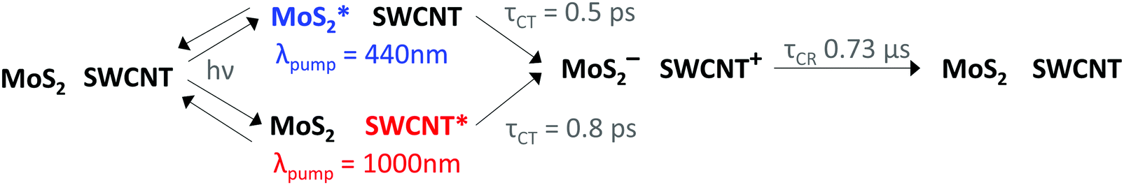 | ||
| Fig. 5 Kinetic scheme highlighting the different time constants for hole transfer (τHT) versus electron transfer (τET) resulting from either selective MoS2 or SWCNT excitation using pump wavelengths (λpump) of 440 and 1000 nm, as well as the time constant for charge recombination (τCR) from the amplitude-averaged lifetime of a triexponential fit. | ||
Charge transfer quantum yield
Quantifying and optimizing charge transfer yield (ϕCT) is crucial for targeted design of interfaces supporting high quantum efficiencies for charge separation. ϕCT is defined as the number of separated charges (Ne or Nh) produced per photogenerated exciton (Nx, taken as the number of absorbed photons). For example, the electron transfer yield is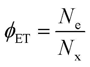 . We estimate charge transfer yields for the Type-II MoS2/SWCNT heterojunctions using two separate methods. One method utilizes an empirically-determined absorption cross section of the (6,5)SWCNT trion induced absorption,50 which in turn is based on the carrier density dependence of the S11 bleaching intensity proposed by Mouri and Matsuda.59 The other method is based on the expected MoS2 exciton bleaching in the presence of charge carriers according to a phase-space filling model for quantum-confined excitons in two-dimensional semiconductors.4
For the first method, we use the intensity of the trion induced absorption relative to the ground-state S11 absorption to estimate ϕET ≈ 23% following selective SWCNT excitation at 1000 nm.50 In the case of hole transfer, we consider both the fraction of 440 nm light absorbed by MoS2 and the much smaller fraction of light absorbed by SWCNTs. We estimate ϕHT ≈ 39%, assuming that both hole transfer and electron transfer proceed concomitantly, and the small amount of SWCNT excitons that undergo electron transfer to MoS2 dissociate with the same 23% yield that we observe under 1000 nm excitation. The 39% hole-transfer yield corresponds to 94% of the Nh hole density originating from MoS2 excitations while SWCNT exciton dissociation accounts for the remaining 6%. We provide fits of the SWCNT trion induced absorption and further discussion of this method for estimating charge-transfer yield in the ESI.†
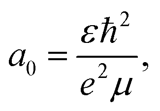
We further investigate a fully independent method for estimating the hole transfer quantum yield based on a phase-space filling model derived from the 2D exciton Schrödinger equation,4 which we apply to the MoS2 bleach amplitude. This method models carrier-induced exciton bleaching using the Pauli exclusion principle, where excess electrons occupying the MoS2 conduction band (e.g. those from charge transfer) block additional transitions from the ground state, thereby decreasing exciton oscillator strength. By representing the exciton as an isolated state in an ideal quantum well and assuming its wavefunction is minimally affected by carrier density, a known solution to the Schrödinger equation can be used and the magnitude of exciton bleaching can be related to physical MoS2 properties such as the dielectric constant (ε), reduced exciton mass (μ), and effective Bohr radius (a0).4
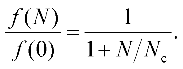
The phase-space filling model gives the fractional decrease in exciton oscillator strength (f) due to a density of N charge carriers as4
 | (1) |
 | (2) |
We estimate the magnitude of carrier-induced bleaching for the MoS2 A exciton transition (660 nm) at the time when charge transfer is complete and all ground state beaching should be due to the presence of charge carriers. We use the MoS2-associated spectral components from global target analysis of the heterojunction following 440 nm excitation, which are shown in Fig. 6A. We provide additional discussion of these species-associated spectral shapes and their kinetics in the ESI.† In brief, we associate the earliest component with decay of the initial singlet population with a 0.9 ps time constant, and we associate the longer-lived components with charge carriers (31 ps and >5 ns decay constants). We estimate charge-induced bleaching by the amplitude of the 660 nm bleach when the initial charge-associated component reaches its maximum concentration (∼3.5 ps). We evaluate f(N)/f(0) using the ground-state absorption A and transient absorption ΔA from Fig. 6A as (A − ΔA)/A = 0.94. In Fig. 6B, we demonstrate the intersection between this magnitude of exciton bleaching that we observe in the TA data with the phase-space filling model.
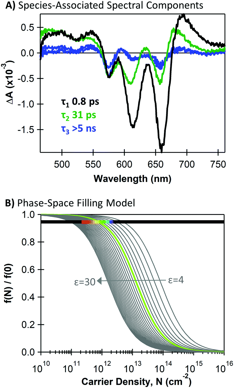 | ||
| Fig. 6 (A) Species-associated components for an MoS2/SWCNT heterojunction under 440 nm excitation from global target analysis using a sequential model with decay time constants given for each component; (B) charge density (N) dependence of the exciton oscillator strength (f) from a phase-space filling model described in ref. 4, plotted for varying dielectric constants and overlaid with a horizontal line at the exciton quenching value from transient absorption analysis (f(N)/f(0) = 0.94). The rainbow section spans carrier densities corresponding to charge-transfer quantum yields of red = 10% to purple = 100%. The green f(N)/f(0) trace corresponds to a 39% charge-transfer yield. | ||
Importantly, eqn (1) and (2) show that the magnitude of carrier-induced exciton bleaching depends on the dielectric constant and the exciton mass, which influence the exciton size in opposite ways. For Fig. 6B, we use an average reduced exciton mass from the literature of 0.25me (where me is the electron mass),33,34,60–63 and we display multiple plots with dielectric constants ranging from 4–30.5,63–66 The horizontal line in Fig. 6B represents the magnitude of carrier-induced exciton bleaching that we observe in our TA data of f(N)/f(0) = 0.94. We highlight a region of this horizontal line with a rainbow gradient indicating the range of possible photogenerated carrier densities with red at 10% charge-transfer quantum yield and purple at 100%. The 10–100% range intersects the f(N)/f(0) traces with dielectric constants of ε = 19 (for 10% yield) and ε = 8 (for 100% yield). The green curve highlights 39% charge-transfer quantum yield (corresponding to ε = 10 and a0 = 2.2 nm), matching our estimate of hole-transfer yield from the SWCNT trion induced absorption.
We note that determining an appropriate value for the dielectric constant experienced by an exciton in monolayer MoS2 is not trivial,5,64–66 and the trends in Fig. 6B highlight its significant impact on the magnitude of carrier-induced exciton bleaching. The dielectric constant of monolayer MoS2 has been the topic of many theoretical and experimental investigations, and values vary considerably depending on MoS2 thickness, sample plane, substrate, defects, and growth methods.5,64–66 Indeed, literature values of MoS2 monolayer dielectric constants5,63–66 vary much more substantially compared to values for exciton mass.33,34,60–63 Importantly, Fig. 6B shows that our observed exciton bleaching from TA measurements does intersect the phase-space filling model at realistic charge-transfer quantum yields with reasonable MoS2 materials parameters, though the uncertainty in the dielectric constant prevents us from confidently extracting a value for charge-transfer quantum yield from this model. Further evaluation of the phase-space filling model and its applicability to monolayer TMDCs could enable this as a new method for using optical signatures to compare dielectric environments across different TMDCs or fabrication methods. In general, accurately estimating charge transfer yield for nanoscale heterojunctions such as these is non-trivial and should be the subject of continued investigation and refinement.
Conclusions
The 0.5 ps hole-transfer time constant (τHT) that we observe at the monolayer MoS2/SWCNT interfaces is on par with or even faster than recently-reported time constants for hole transfer in organic/MoS2 heterojunctions, including pentacene/MoS2 with τHT ≈ 6.7 ps44 and polymer (PTB7)/MoS2 with τHT ≈ 1–5 ps.42 In addition to this faster hole transfer time, an important advantage of SWCNT/MoS2 heterojunction systems over polymer or small molecule heterojunctions is the exceptional chemical and photo-stability of the SWCNTs, implying that this type of heterojunction is a truly viable option for photocatalytic systems where photons can drive hydrogen evolution in aqueous environments at low pH (high proton concentrations). While TMDC/TMDC heterojunctions may promise even faster hole transfer times, it is important to note that charge transfer in these systems is characterized by the formation of tightly bound interfacial excitons that decay rapidly on picosecond time scales, as carriers are spatially confined and have limited ability to move away from the interface.37The 0.8 ps electron-transfer time (τET) for the monolayer MoS2/SWCNT system is slightly slower than that at TMDC/TMDC and other MoS2/organic heterojunctions. We attribute the slower τET to the low driving force for SWCNT exciton separation and subsequent charge transfer to monolayer MoS2. With sufficient driving force, interfacial electron transfer following SWCNT exciton dissociation can occur on faster time scales (<120 fs) and with correspondingly higher yields.50 In the current model system, we suspect that the charge-transfer yield could be optimized through many avenues such as (1) increasing the driving force and carrier delocalization either by using nanotubes with different diameters or TMDCs with higher electron affinity; (2) exploring the effect of TMDC defect density, lateral continuity, layer number, and internal strain on charge transfer kinetics and yield; (3) increasing the thickness of the SWCNT layer to support longer range charge separation; (4) tuning the effective MoS2 dielectric constant; or (5) altering the SWCNT/TMDC interface by doping of either or both semiconductor.
Optimizing the charge-transfer yield, in conjunction with maintaining or increasing the already exceptionally long 0.73 μs carrier lifetimes, could enable efficient photocurrent generation and hydrogen evolution devices employing these interfaces. Importantly, the 0.73 μs lifetime of charge-separated states in the MoS2/SWCNT heterojunctions is to our knowledge orders of magnitude longer than lifetimes for charge-separated states in other TMDC systems.42,44 To a large extent, we credit the long lifetime to the excellent ability of the SWCNT layer to sustain and delocalize charge, allowing carriers to efficiently move away from the MoS2 interface. Indeed, organic heterojunctions employing SWCNT films have also achieved lifetimes exceeding 1 μs.14 It is also possible that the SWCNT layer helps to decrease carrier trapping by passivating MoS2 surface defects, as has previously been proposed for other organic/TMDC interfaces.67
Our study demonstrates the promise of pairing TMDCs with SWCNTs both for enabling functional applications requiring ultrafast charge generation and exceptionally long-lived carriers as well as for use as a clean model system for optical studies of TMDCs based on well-characterized and clearly resolvable SWCNT spectral signatures. Future studies of TMDC/SWCNT heterojunctions should probe the roles of both in-plane and out-of-plane carrier delocalization and/or diffusion in stabilizing long-lived charges. The well-defined SWCNT charge-associated signatures should also be useful for probing the roles of thermodynamic driving force and dielectric environment on charge separation and recombination in a variety of TMDCs.
Conflicts of interest
There are no conflicts to declare.Acknowledgements
This work was authored by the National Renewable Energy Laboratory, operated by Alliance for Sustainable Energy, LLC, for the U.S. Department of Energy (DOE) under Contract No. DE-AC36-08GO28308. Funding provided by the Solar Photochemistry Program of the Chemical Sciences, Geosciences, & Biosciences (CSGB) Division at the U.S. DOE Office of Science: Basic Energy Sciences. The views expressed in the article do not necessarily represent the views of the DOE or the U.S. Government.References
- H. Li, C. Tsai, A. L. Koh, L. Cai, A. W. Contryman, A. H. Fragapane, J. Zhao, H. S. Han, H. C. Manoharan, F. Abild-Pedersen, J. K. Nørskov and X. Zheng, Nat. Mater., 2015, 15, 48 CrossRef.
- H. Huang, W. Huang, Z. Yang, J. Huang, J. Lin, W. Liu and Y. Liu, J. Mater. Chem. A, 2017, 5, 1558 RSC.
- X. Han, X. Tong, X. Liu, A. Chen, X. Wen, N. Yang and X.-Y. Guo, ACS Catal., 2018, 8, 1828 CrossRef CAS.
- D. Huang, J.-I. Chyi and H. Morkoç, Phys. Rev. B: Condens. Matter Mater. Phys., 1990, 42, 5147 CrossRef CAS.
- S. Park, N. Mutz, T. Schultz, S. Blumstengel, A. Han, A. Aljarb, L.-J. Li, E. J. W. List-Kratochvil, P. Amsalem and N. Koch, 2D Mater., 2018, 5, 025003 CrossRef.
- F. Davoodi and N. Granpayeh, Opt. Quantum Electron., 2018, 51, 9 CrossRef.
- B. Radisavljevic, A. Radenovic, J. Brivio, V. Giacometti and A. Kis, Nat. Nanotechnol., 2011, 6, 147 CrossRef CAS PubMed.
- H. Wang, L. Yu, Y.-H. Lee, Y. Shi, A. Hsu, M. L. Chin, L.-J. Li, M. Dubey, J. Kong and T. Palacios, Nano Lett., 2012, 12, 4674 CrossRef CAS.
- Y. Liu, J. Guo, E. Zhu, L. Liao, S.-J. Lee, M. Ding, I. Shakir, V. Gambin, Y. Huang and X. Duan, Nature, 2018, 557, 696 CrossRef CAS.
- M. Bernardi, M. Palummo and J. C. Grossman, Nano Lett., 2013, 13, 3664 CrossRef CAS.
- Y. Zhang, H. Yu, R. Zhang, G. Zhao, H. Zhang, Y. Chen, L. Mei, M. Tonelli and J. Wang, Opt. Lett., 2017, 42, 547 CrossRef CAS.
- T. A. Shastry, I. Balla, H. Bergeron, S. H. Amsterdam, T. J. Marks and M. C. Hersam, ACS Nano, 2016, 10, 10573 CrossRef CAS.
- J. Wong, D. Jariwala, G. Tagliabue, K. Tat, A. R. Davoyan, M. C. Sherrott and H. A. Atwater, ACS Nano, 2017, 11, 7230 CrossRef.
- H. S. Kang, T. J. Sisto, S. Peurifoy, D. H. Arias, B. Zhang, C. Nuckolls and J. L. Blackburn, J. Phys. Chem. C, 2018, 122, 14150 CrossRef CAS.
- R. G. Dickinson and L. Pauling, J. Am. Chem. Soc., 1923, 45, 1466 CrossRef CAS.
- P. Joensen, R. F. Frindt and S. R. Morrison, Mater. Res. Bull., 1986, 21, 457 CrossRef CAS.
- M. J. Allen, V. C. Tung and R. B. Kaner, Chem. Rev., 2010, 110, 132 CrossRef CAS.
- S. Manzeli, D. Ovchinnikov, D. Pasquier, O. V. Yazyev and A. Kis, Nat. Rev. Mater., 2017, 2, 17033 CrossRef CAS.
- W. Choi, N. Choudhary, G. H. Han, J. Park, D. Akinwande and Y. H. Lee, Mater. Today, 2017, 20, 116 CrossRef CAS.
- A. Splendiani, L. Sun, Y. Zhang, T. Li, J. Kim, C.-Y. Chim, G. Galli and F. Wang, Nano Lett., 2010, 10, 1271 CrossRef CAS.
- K. F. Mak, C. Lee, J. Hone, J. Shan and T. F. Heinz, Phys. Rev. Lett., 2010, 105, 136805 CrossRef.
- S. Pak, J. Lee, Y.-W. Lee, A. R. Jang, S. Ahn, K. Y. Ma, Y. Cho, J. Hong, S. Lee, H. Y. Jeong, H. Im, H. S. Shin, S. M. Morris, S. Cha, J. I. Sohn and J. M. Kim, Nano Lett., 2017, 17, 5634 CrossRef CAS.
- Y. Sun and K. Liu, J. Appl. Phys., 2018, 125, 082402 CrossRef.
- H. Nan, Z. Wang, W. Wang, Z. Liang, Y. Lu, Q. Chen, D. He, P. Tan, F. Miao, X. Wang, J. Wang and Z. Ni, ACS Nano, 2014, 8, 5738 CrossRef CAS.
- S. Mouri, Y. Miyauchi and K. Matsuda, Nano Lett., 2013, 13, 5944 CrossRef CAS.
- X. Xu, W. Yao, D. Xiao and T. F. Heinz, Nat. Phys., 2014, 10, 343 Search PubMed.
- D. Xiao, G.-B. Liu, W. Feng, X. Xu and W. Yao, Phys. Rev. Lett., 2012, 108, 196802 CrossRef.
- Z.-Z. Zhang, X.-X. Song, G. Luo, G.-W. Deng, V. Mosallanejad, T. Taniguchi, K. Watanabe, H.-O. Li, G. Cao, G.-C. Guo, F. Nori and G.-P. Guo, Sci. Adv., 2017, 3, e1701699 CrossRef.
- J. G. Roch, N. Leisgang, G. Froehlicher, P. Makk, K. Watanabe, T. Taniguchi, C. Schönenberger and R. J. Warburton, Nano Lett., 2018, 18, 1070 CrossRef CAS.
- M. N. Ali, J. Xiong, S. Flynn, J. Tao, Q. D. Gibson, L. M. Schoop, T. Liang, N. Haldolaarachchige, M. Hirschberger, N. P. Ong and R. J. Cava, Nature, 2014, 514, 205 CrossRef CAS PubMed.
- D. Kang, Y. Zhou, W. Yi, C. Yang, J. Guo, Y. Shi, S. Zhang, Z. Wang, C. Zhang, S. Jiang, A. Li, K. Yang, Q. Wu, G. Zhang, L. Sun and Z. Zhao, Nat. Commun., 2015, 6, 7804 CrossRef.
- M. Khezerlou and H. Goudarzi, Phys. Rev. B, 2016, 93, 115406 CrossRef.
- S. Latini, K. T. Winther, T. Olsen and K. S. Thygesen, Nano Lett., 2017, 17, 938 CrossRef CAS.
- A. Thilagam, J. Appl. Phys., 2014, 116, 053523 CrossRef.
- D. Vella, D. Ovchinnikov, D. Viola, D. Dumcenco, Y. C. Kung, E. A. A. Pogna, S. D. Conte, V. Vega-Mayoral, T. Borzda, M. Prijatelj, D. Mihailovic, A. Kis, G. Cerullo and C. Gadermaier, 2D Mater., 2017, 4, 035017 CrossRef.
- D. Vikraman, S. Hussain, K. Akbar, L. Truong, A. Kathalingam, S.-H. Chun, J. Jung, H. J. Park and H.-S. Kim, ACS Sustainable Chem. Eng., 2018, 6, 8400 CrossRef CAS.
- X. Hong, J. Kim, S.-F. Shi, Y. Zhang, C. Jin, Y. Sun, S. Tongay, J. Wu, Y. Zhang and F. Wang, Nat. Nanotechnol., 2014, 9, 682 CrossRef CAS.
- M. Tosun, D. Fu, S. B. Desai, C. Ko, J. Seuk Kang, D.-H. Lien, M. Najmzadeh, S. Tongay, J. Wu and A. Javey, Sci. Rep., 2015, 5, 10990 CrossRef.
- S. L. Howell, D. Jariwala, C.-C. Wu, K.-S. Chen, V. K. Sangwan, J. Kang, T. J. Marks, M. C. Hersam and L. J. Lauhon, Nano Lett., 2015, 15, 2278 CrossRef CAS PubMed.
- Y. Yang, N. Huo and J. Li, J. Mater. Chem. C, 2017, 5, 7051 RSC.
- T. R. Kafle, B. Kattel, S. D. Lane, T. Wang, H. Zhao and W.-L. Chan, ACS Nano, 2017, 11, 10184 CrossRef CAS PubMed.
- C. Zhong, V. K. Sangwan, C. Wang, H. Bergeron, M. C. Hersam and E. A. Weiss, J. Phys. Chem. Lett., 2018, 9, 2484 CrossRef CAS.
- Y. L. Huang, Y. J. Zheng, Z. Song, D. Chi, A. T. S. Wee and S. Y. Quek, Chem. Soc. Rev., 2018, 47, 3241 RSC.
- S. Bettis Homan, V. K. Sangwan, I. Balla, H. Bergeron, E. A. Weiss and M. C. Hersam, Nano Lett., 2017, 17, 164 CrossRef CAS.
- T. Guo, S. Sampat, K. Zhang, J. A. Robinson, S. M. Rupich, Y. J. Chabal, Y. N. Gartstein and A. V. Malko, Sci. Rep., 2017, 7, 41967 CrossRef CAS.
- M.-L. Tsai, S.-H. Su, J.-K. Chang, D.-S. Tsai, C.-H. Chen, C.-I. Wu, L.-J. Li, L.-J. Chen and J.-H. He, ACS Nano, 2014, 8, 8317 CrossRef CAS.
- X. Qian, J. Ding, J. Zhang, Y. Zhang, Y. Wang, E. Kan, X. Wang and J. Zhu, Nanoscale, 2018, 10, 1766 RSC.
- Z. Zhang, W.-Q. Huang, Z. Xie, W. Hu, P. Peng and G.-F. Huang, J. Phys. Chem. C, 2017, 121, 21921 CrossRef CAS.
- P. Li, Z. Yang, J. Shen, H. Nie, Q. Cai, L. Li, M. Ge, C. Gu, X. A. Chen, K. Yang, L. Zhang, Y. Chen and S. Huang, ACS Appl. Mater. Interfaces, 2016, 8, 3543 CrossRef CAS.
- A.-M. Dowgiallo, K. S. Mistry, J. C. Johnson and J. L. Blackburn, ACS Nano, 2014, 8, 8573 CrossRef CAS.
- R. Ihly, K. S. Mistry, A. J. Ferguson, T. T. Clikeman, B. W. Larson, O. Reid, O. V. Boltalina, S. H. Strauss, G. Rumbles and J. L. Blackburn, Nat. Chem., 2016, 8, 603 CrossRef CAS.
- W. Rui, W. Tianjiao, H. Tu and X. Ya-Qiong, Nanotechnology, 2018, 29, 345205 CrossRef.
- D. Jariwala, V. K. Sangwan, C.-C. Wu, P. L. Prabhumirashi, M. L. Geier, T. J. Marks, L. J. Lauhon and M. C. Hersam, Proc. Natl. Acad. Sci. U. S. A., 2013, 110, 18076 CrossRef CAS.
- J. J. Snellenburg, S. Laptenok, R. Seger, K. M. Mullen and I. H. M. van Stokkum, J. Stat. Softw., 2012, 49, 1 Search PubMed.
- M. Zdrojek, T. Mélin, H. Diesinger, D. Stiévenard, W. Gebicki and L. Adamowicz, J. Appl. Phys., 2006, 100, 114326 CrossRef.
- T. Dürkop, S. Getty, E. Cobas and M. Fuhrer, Nano Lett., 2004, 4, 35 CrossRef.
- D. C. Coffey, B. W. Larson, A. W. Hains, J. B. Whitaker, N. Kopidakis, O. V. Boltalina, S. H. Strauss and G. Rumbles, J. Phys. Chem. C, 2012, 116, 8916 CrossRef CAS.
- Y. Yu, C. Li, Y. Liu, L. Su, Y. Zhang and L. Cao, Sci. Rep., 2013, 3, 1866 CrossRef.
- S. Mouri and K. Matsuda, J. Appl. Phys., 2012, 111, 094309 CrossRef.
- A. Ramasubramaniam, Phys. Rev. B: Condens. Matter Mater. Phys., 2012, 86, 115409 CrossRef.
- F. A. Rasmussen and K. S. Thygesen, J. Phys. Chem. C, 2015, 119, 13169 CrossRef CAS.
- T. C. Berkelbach, M. S. Hybertsen and D. R. Reichman, Phys. Rev. B: Condens. Matter Mater. Phys., 2013, 88, 045318 CrossRef.
- Y. Yu, Y. Yu, Y. Cai, W. Li, A. Gurarslan, H. Peelaers, D. E. Aspnes, C. G. Van de Walle, N. V. Nguyen, Y.-W. Zhang and L. Cao, Sci. Rep., 2015, 5, 16996 CrossRef CAS.
- S.-L. Li, K. Tsukagoshi, E. Orgiu and P. Samorì, Chem. Soc. Rev., 2016, 45, 118 RSC.
- A. Laturia, M. L. Van de Put and W. G. Vandenberghe, npj 2D Mater. Appl., 2018, 2, 6 CrossRef.
- E. J. G. Santos and E. Kaxiras, ACS Nano, 2013, 7, 10741 CrossRef CAS.
- J. H. Park, A. Sanne, Y. Guo, M. Amani, K. Zhang, H. C. P. Movva, J. A. Robinson, A. Javey, J. Robertson, S. K. Banerjee and A. C. Kummel, Sci. Adv., 2017, 3, e1701661 CrossRef.
Footnote |
| † Electronic supplementary information (ESI) available: Materials and methods. See DOI: 10.1039/c9mh00954j |
| This journal is © The Royal Society of Chemistry 2019 |